Note: Descriptions are shown in the official language in which they were submitted.
1 3 1 0762
ARBITRATION TECHNIQUE FOR A SPLIT TRANSACTION
BUS IN A ~LTIPROCESSOR COMPUTER SYSTEM
This is a division of copending Canadian application
547,1~0 filed September 17, 1987.
The present invention pertains to a new and improved
synchronous, transaction arbitrated, split transaction bus
~or advantageous use in a tightly coupled multiprocessor
computer system to attain data transfers of high aggregate
1~ throughput shared fairly among a plurality of initiators
(a~. processors) and responders (e.g. memories) as a result
o~ an improved arbitration technique.
a~ie~ Backqround of the Invention
1~
In a computer system, a bus is the means by which the
~lect~ical signals are communicated back and forth between a
c~ntral processor, mèmory, and other devices such as input
nnd output adapters. In a uniprocessor computer system, the
2~ bus ~ay simply be a plurality o~ electrical conductors
linking the various components oE the system. ~owever, in
~ultiprocessor and other more sophisticated computer systems,
the ~us may beco~e more complex and play an active role in
d~ ting the various signals between the components of the
c~mput~r system, usually ~or the purpose o~ obtainin~ greater
d~t~ throuqhput or speed o~ operation.
one o~ the significant restrictions in the operation
O~ ~ mode~n hi~h speed computer is the memory access time of
m~n m~moxy. The me~ory access time is that time required
39 ~ar the ~ory to retrieve the in~ormation from
131U-/62
its internal storage after it has received a read address
signal. Since a high percentage of data processing
activities in a computer system involves reading informa~
~ion from memory, the cumulative amount of memory`access
time involved in typical data processin~ activities can
be significant. The cumulative effect of the waiting
during access time periods is to reduce the data
throughput of the computer system. In a uniprocessor
computer system, the system is inactive during the memory
1~ a~cess time because the processor is waiting on a
~e~ponse from the memory during the memory access time.
In a uniprocessor system, this is not particularly a
problem because there is nothing else which the system
could be doing during the access time period. However,
in multiprocessor systems, the other processors in the
system could use the access time periods to conduct other
activities, and thereby increase the throughput of the
system.
~hese problems have been recognized and, as a
~0 result~ split transaction buses have been devised. In a
split transaction bus, the bus is arranged to communicate
rend address signal from the initiator (e.g. processor)
to the responder (e.g. memory) in a separate transaction
from that transaction which is delayed in time during
2~ whi~h the addressed memory transfers or communicates the
read data information from its internal memory back to
-2-
. .
1 3 1 0762
the initiator. During the time period which elapses
between the read address signal and the response from ~he
memory, the other processors in the computer system are
communicating otller signals to other components o~ the
system over the bus.
In order to avoid the confusion resulting from con-
flicting communications between the various components of
the computer system, an arbitration technique is neces-
sary in each split transaction bus. The arbitration
technique determines which one of the particular compo-
nents o~ the system has exclusive access to the bus at
any particular time. The time intervals during which
;nformation can be communicated over the bus are known as
bus cycles. In order to resolve competinq requests to
15 use the bus, each of the components of the system must be
assi~ned a priority.
One typical approach to bus arbitration is known as
activity arbitration, in which a higher priority s~ystem
component is given exclusive access to the bus for a suf-
ficient number of bus cycles or time in order to conclude
any particular activity. The disadvantage of activity
arbitrated buses is that the higher priority component
m~y retain access to the bus for a sufficiently long time
~eriod and prevent other components from being able to
transfer information, thereby losing that information.
~nother type of arbitration techni~ue is cycle
7 6 2
arbitration, in which each and every cycle of the bus is
individually arbitrated. The disadvantage of cycle arbi-
tration is that an excessive amount of time is consumed
in individually arbitrating each and every cycle, which
can result in a reduced information throughput.
Cycle arbitration is particularly time consuming on
systems utilizing centralized arbitration. In central-
ize~ arbitration systems, a single processor or other
component resolves all competing requests for use of the
10 bus and determines which o`f the individual components is
qiven access to the bus. Centralized arbitration usually
re~uires the competing system components to communicate
request signals to the centralized arbiter, and the cen-
trali~ed arbiter to communicate the signals giving a par-
15 ticular component access to the bus after the arbitrationha~ been determined. This process, known as
"handshaking" also consumes time during which no usable
information can be communicated over the bus. Such cen-
trali2ed arbitration techniques there~ore also tend to
reduce the capacity for data transfer, known as
n~andwidth" of the bus.
~ istributed arbitration techniques have been devised
to avoid the problems associated with centralized arbi-
tration. In a distributed arbitration system, each indi-
25 v;dual component of the computer system includes its owncircuitry or logic to arbitratè the requests from all of
1 3 1 0762
the system components and determine which component is
given exclusive access to the bus during a particular bus
cycle. Distributed arbitration techniques usually
involve less time consumptive activities on the bus
itself and increase the capacity of the bus.
At the present time, synchronous buses also contrib-
ute to higher bus capacity. A synchronous bus is one in
which all information transfers take place in synchronism
with a single clock signal. An asynchronous bus is one
10 in which the activities on the bus are not clocked at
regular intervals. With a synchronous bus, there will
generally be a higher information capacity because the
~locked synchronism of all transfers of information oper-
ate on the assumption that the component receiving the
15 in~ormation will have in fact received it. In contrast,
an asynchronous bus requires that the component receiving
the information send back a sisnal acknowledging its
receipt. The separate acknowledgement signal also uti-
li~es bus capacity without contributing to data
~0 throughput. So long as memory cycle times, that is the
memory access time plus that additional minimum time
; required to respond to the next successive read address
signal, are substantially greater than the bus cycle
~ime, a higher data throughput will be obtained Erom
~5 synchronous buses than from asynchronous buses. Tradi-
tionally, synchronous buses have also been more reliable
_5_
~ 3 t ~762
because the operation of the bus can be checked by
sampling signals at given points in time and looking for
inconsistencies in the sampled signal. Lastly, and per-
haps most importantly, synchronous buses allow the imple-
mentation of sophisticated arbitration techniques. In anasynchronous bus, there is very li~tle, if any, arbitra-
tion, since requests for use of the bus will be resolved
on a basis of which request is received first in time.
In synchronous buses, more sophisticated determinations
can be implemented because requests are sampled at
selected fixed points in time rather than aperiodically,
and competing requests can be resolved on the basis of
priority of importance assigned to the particular system
component generating the request.
Brief Summary o the Invention
In significant respects, the present invention
relates to improvements in the arbitration technique
employed in a synchronous, split transaction bus. The
arbitration technique of the present invention assigns
unique priority designations to each of the plurality of
modules or components in the computer system. This
assigned priority is used to resolve competing conten-
tions or collisions between different modules requesting
e~clusive access or "mastership" of the bus. The arbi-
~5 tration technique also involves discrimination between"initiator" modules which initiate transactions over the
--6--
1 3 1 0762
bus, such as processors or input~output devices, and
"responder" modules which respond to the initiators, such
as memories.
In the arbitration technique of the present inven~
tion, responders are given priority over initiators,
based on the premise that the delay times will be reduced
and the data throughput ~ill be increased by not delayin~
the responses to waiting initiators any longer than is
necessary for the responders to supply the information
which the initiators have`previously requested. 80th the
initiators and the responders will become more active and
in~ur less wait states as a result. Competitions for
mastership between responders are resolved on the prior-
;ty basis designated to each module. Such fixed priority
arbitration between responders cannot result in one
responder '`monopolizing" the bus to the detriment of
~ther responders because responders perform bus activity
solely in response to previous bus activity by
~` initiators.
2~The arbitration of competing requests by initiators
- im~oses l'fairness" to prevent faster, or higher priority,
ini~i~tors from utilizing so much bus bandwidth that
l~w~r priority, or slower, initiators are unable to oper-
a~ ef}ec~ively. The arbitration fairness assigns bus
2~ mastership to competing initiators based on fixed
priorities for requests arriving during a given bus
,
~ _7- ~
r
~`; ' ' ., .
` . .
~ ~ I
1 3 1 0762
cycle. All requests from initiators arriving during any
given cycle are handled, in priority sequence, before any
request~ from initiators arriving during subsequent
cycles.
Initiators which address busy responders, that is a
responder which is involved in currently responding to a
previous request from another initiator, are supplied
with an indication when the responder is no longer busy.
Until such indication is supplied, a re-try to that par-
ticular module is deferred until there is an opportunitythat the particular module can accept the initiator's
request. In order to expedite such re-try activities,
requests from non-retrying initiators are temporarily
rescinded when a responder indicates that it is ready to
receive a re-try
Transactions as opposed to transfers over the bus
are arbitrated. Each transaction can consume up to a
` maximum predetermined number of bus cycles, and the maxi-
mum number of bus cycles is selected so that no particu-
lar module will monopolize the bus for such an excessive
amount of time that other information might be lost rom
other modules. For tra~nsactions which require more than
one bus cycle, a signal indicating that the bus is to be
held for more than one consecutive cycle is delivered to
25 defer arbitration until completion of the previous trans-
action. Each of the modules inciudes its own distributed
arbiter for resolving the mastership of the bus.
-8-
1 3 1 0762
A relatively high aggregate data throughput is
obtained from the present invention as a result of
eliminating the equal competition between initiators and
responders for bus mastership. By giving the responders
precedence over the initiators, the initiators become active
sooner upon receiving the information previously requested
from the responders. By signaling waiting initiators that a
pre~iously busy responder has become available and is no
longer busy, and giving retrying initiators precedence over
non-retrying initiators, bus bandwidth is not excessively
wasted on useless retries, as is the case with arbitrarily
initiated re-try requests common in some prior buses.
~imilarly, bus capacity is expanded and more evenly
distributed among the modules, by deferring all subsequent
xequests until the previous requests have been serviced in
prioxity order. By arbitrating on the basis of individual
~x~nsactions, as opposed to activities or bus cycles, data
thxo~lghput is also increased.
Therefore, in accordance with the present invention
the~e is provided in a computer system havin~ initiator
~odules including at least one processor and also having
responder modules including at least one memory, a bus
co~only connecting the modules, means for establishing bus
~ycles during which separate transfers of information are
com~unicated between the modules, and means for arbitrating
m~stexship of the bus to establish selected communication
path~ bet~aen an initiator and a responder; an improved means
~r ~cco~plishing test and set memory operations~ The
i~pxoved means comprise in combination: means for
~r~ns~erxing a read/modify/write command to the memory during
~n~ bus cycle, and wherein: the memory further includes means
~3~ ~r~or~in~ a read/modify/write operation in
1370762
response to the read/modify/write command and for
transferring data back during a different bus cycl~
subsequent to the one bus cycle; and the bus arbitrating
means inhibiting communication to the memory being tested and
set until a bus cycle after the different bus cycle.
These factors and others contribute to the
i~provements available from the present invention. The
present invention can be understood more completely by
~ r~ing to the accompanying detailed description of a
1~ p~esently preferred embodiment of the invention, and the
accompanying drawings~ Of course, the scope of the invention
i~self is defined by the sppended claims.
.
::
~ :
~ `
i
- 9a -
~'
t
.. ~
~" ' '
~'
1 31 3762
Brief Description of the Drawinqs
.
Fig. 1 is a block diagram illustrating a computer
system which incorporates a plurality of processor
modules, a plurality of input/output adapter moduies, a
S plurality of main memory modules, a plurality of special
purpose memory modules, and the improved bus of the
present invention.
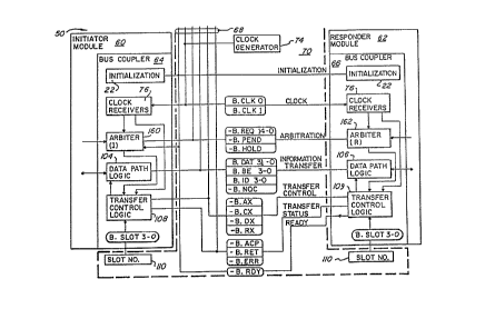
Fig. 2 is a block diagram of the bus of the present
invention shown in Fig. 1, illustrating certain signifi-
10 cant signals conducted over the bus and portions of aninitiator module and a responder module which are also
shown in Fig. 1.
Figs. 3A, 3B, 3C, 3D, 3E, 3F, 3~, 3I, 3J, 3~, 3L,
3M, and 3N are timing wave form diagrams illustrating bus
lS cycles, components of bus cycles, and the timing of
various signals on the bus which are illustrated in Fig.
2. Fig. 3G designates separate bus cycles and states of
each bus cycle.
Fig. 4 is a logic circuit diagram of a clock
~o receiver of each bus coupler of the bus shown in Fig. 2.
; Fig. 5A is an illustration of a doubleword which may
be transferred over the bus of the present invention as
the basic unit of data transfer in a single transaction,
and Fig. 5B illustrates four doublewords which are the
25 maximum number of doublewords which may be transferred
over the bus in a single transaction.
--10--
~ 3 ~ 0762
Figs. 6A, ~B, 6C, 6D and 6E are illustrations of
data write, data read, test and set and memory scrub,
control write, and control read transactions, respec-
tively, which may occur over the bus of the present
invention, illustrated with reference to the number and
spacial time relationship of various bus cycles during
which transfers of these transactions occur.
Figs~ 7A, 78 and 7C are illustrations of the bit
~ormats of an address, a read and write data and a con-
trol doubleword which may be transferred over the bus ofthe present invention during the various transactions
illustrated in Fig. 6.
Fig~ 8 is a block diagram of an initiator data path
logic element shown in Fig. 2~
lS Fig~ 9 is a block diagram of a responder data path
logic element shown in Fig~ 2~
Fig~ 10 is a chart illustrating the split transac-
tion nature of operation of the bus shown in Fig. 2, with
respect to the arbitration signals, information transfer
and transfer control signals, and transfer of status
~ signals, during successive cycles of the bus, under a
: vnriety ~f diferent arbitration situations~
Fig~ 11 is a timing diagram illustrating an example
o~ m~ltiple requests and the resolution thereof, among
. ~ ~5 other things, under the arbitration technique of the
present invention.
.
1 3 1 ~762
Fig. 12 is a timing diagram illustrating an e~ample
of a rescinded request, among other things, under the
arbitration technique of the present invention.
Fig~ 13 is a timing diagram illustrating an example
of multiple re-trying, among other things, initiators
under the arbitration technique of the present invention.
Fig. 1~ is a timing diagram illustrating an example
of multiple re-trys by one initiator, among other things,
under the arbitration technique of the present invention.
Figs. 11 to 1~ employ arrows connecting various
signals to indicate conditions giving rise to causative
events. The circles at the tails of the arrows represent
the various conditions which create or cause the situa-
tion indicated at the head of the arrow.
Fig. 15 is a generalized representation of pin con-
nectors for connecting each of the modules shown in Fig.
1 into a mother board or back plane of the bus, and fur-
ther illustrating the means by which request signals from
each module are connected to other modules.
Figs. 16A, 16B and 16C, collectively, are a sche-
matic diagram of the logic circuitry of the arbitration
logic of an initiator of the bus as is shown in Fig. 2.
Figs. 16D, 16B and 16E, collectively, are a sche-
matic diagram of the logic circuitry of the arbitration
25 logic of a responder of the bus as is shown in Fig. 2.
Figs. 16A, 16B, 16C, 16D and 16E are idealized
-12-
,
1 3 1 0762
schematic representations of logic circuitry which differ
in actual implementation only in the sense that certain
additional components are required to achieve compensa-
tion for time and propagation delays when operated at
very high speeds.
Detailed Description
A tightly-coupled multi~rocessor computer system is
illustrated in Fig. 1. The bus of the present invention,
designated 50 in Fig. 1, serves as a high performance
communication means for communicating data, control
10 transfer, control status, and arbitration signals between
a plurality of central processor modules 52, a plurality
of input/output ("I/O") adapter modules 5~, a plurality
of main memory modules 56, ar.d a plurality of special
purpose memory modules 58. The bus 50 allows the plural-
15 ity of processors 52 and I/O adapters 5~ to communicatewith each other and to share a common pool of main 56 and
special purpose 5~ memory. The computer system shown in
Fig. 1 is tightly coupled because its plurality of cen-
tral processor modules 52 communicate over the single bus
SO to a common pool of main memory.
Each of the memory modules 56 and 58 includes con-
ventional memory components. The main memory module 56
is the general purpose memory of the system. The memory
components of the special purpose memory module 58 may
also be conventional, but they may be subject to
-13-
1310762
modification from a source other than that shown in Fig.
1. For example, the special purpose memory modules may
be qraphics memory modules and an external drawing engine
(not shown) may be employed to draw vectors, characters
and other symbols into the graphics memory through a com-
munication path other than over the bus 50. Some or all
of the memories in the modules 56 and 58 may be cache
memories, and cache memories may be included in the pro-
cessor and I/O adapter modules 52 and 5~. Of course, the
overall purpose of each of the memories is to retain data
which has been written or recorded into the memories at
predetermined addresses, and to supply the information
recorded at particular addresses back to some other com-
ponent or module which has requested the information at
the particular address.
,~ Each central processor module 52 includes a conven-
tional processor which manipulates data in the memory.
The processors may also interpret the contents of memory
¦ as speci~ic instructions, data, etc., in order to process
data~
Each I~O adapter module 5~ is connected to an I/O
device ~not shown). Each I/O device may be one of a
variety of different external devices connected to the
computer system. For example, the I/O devices may be a
~5 local area network, another computer such-as a small or
- p~rsonal computer, and a disk memory. Each I/O adapter
: -1~-
.~ .
'
,
.
.,~ , '`
:
~310762
54 presents a uniform electrical interface to the bus 50
in order that communication is established between the
I/O devices through the I/O adapter modules 54 to the
other modules connected to the bus 50.
Each of the modules 52, 54, 56 and 5~ include a
coupler by which signals from the bus are communicated to
the other components of the module, and communications
originating from the other components of the module are
coupled back to the bus through the coupler. The
10 couplers are described in greater detail in Fig. 2 and
are part of the bus 50 as described herein.
The modules attached to the bus 50 are either
"initiators" or "responders". An initiator module and a
responder module are each a particular type of module
15 whose characteristics are established and are incapable
of changing.
An initiator module is one which is capable of
initiating bus activity for the purpose of performing
memory space data transfers in response to exogenous or
internally generated conditions. The central processor
modules 52 and the I/O adapter modules 54 are initiators
and are referenced as such at 60. The processor in each
central processor module 52 initiates bus activity from
internally generated conditions, such as those occurring
in response to the execution of instructions, The I/O
adapter modules 54 initiate bus activity in response to
-15-
,
13~0762
exogenous events such as signals supplied from the I/O
devices.
Responder modules are those which are only capable
of initiating bus activity for the purpose of performing
~ransfers in response to requests issued by initiators.
That is, a responder is capable of initiating bus activ-
ity in response to a previously received bus activity,
and not in response to exogenous events. Thus, the mem-
ory modules 56 and 58 are shown as responders at 62
because they only respond to previous requests by the
initiator modules 52 and 5~.
The responders are interfaced to the bus 50 on a
split transactional basis. The responders receive a read
r~quest signal at one bus cycle or point in time, and at
1~ a later bus cycle or later point in time greater than or
equal to the memory access time and in conjunction with a
specific bus cycle, send the reply back to the initiator.
Because the modules both transmit signals over the
bu~ 50 and receive signals over the bus 50, all of the
modules can function as a "master" at a particular time
and as a "slave" at a different time. At any given time,
the bus S~ is either idle (null~, meaning that no "trans-
~r" or activity is goin~ on over it; or the bus is
a~tive, meanin9 that exactly one "transfer" or activity
is going on over it. During each active bus cycle, one
module functions as a master and one module functions as
-16-
i3~(~76~
a slave. The module functioning as a master is that
module which is driving the transfer and transfer control
signals, and the module functioning as the slave is that
module which is selected to receive the transfer and
transfer control signals driven by the master. The terms
"master" and "slave" are therefore dynamic concepts
related to bus arbitration and usage. For example, when
a processor module 52 is sending a read request to a mem-
ory module 56, the processor module 52 is the master and
10 ~he me~nory module 56 is thè slave. However, when the
mem~ry module S6 is replying to a read request sent pre-
vi-ously by the processor 52, the memory module 56 is the
m~ster and the processor that requested the information
is the slave.
lS With reference to Fig. 1, unlike many computer sys-
tems, there is no physical dedicated connection between
the I~O adapters and the processors. The single shared
bus 50 is the sole means of intercommunication between
all modules o~ the computer system. The communication
~ ~0 b~tween the sotware running on the processor module 52
`~ and an I/O adapter module S~ which will physically per-
}orm the input~outpu~ to an I/O device is through shared
-d~ta structures stored in the main memory on the memory
modules 56. These data structures are used in estab-
lishin9 a uniform communication protocol between all of
~h~ modules connected to the bus 50. One such
-17-
~ , ~
~ 31 0762
:
communication protoco]. is described i.n co-pending
Canadian patent app].ication for an "Input/Output Control
Technique", seria]. number 5~7,198, filed concurrently
herewith and assigned to the assignee hereo~.
More detai].s of the bus 50 are illustrated in Fig.
2. The bus 50 includes an initiator coupler 64 con-
nected to each initiator modu].e 60 and a responder
coupler 66 connected to each responder module 62. The
initiator coupler 64 and the responder coupler 66 are
very simi].ar. Each significant difference will be
described be].ow. Signa].s between the bus coup].ers 64
and 66 of each of the modules are conducted over a
plura].ity of electrical conductors, indicated collec-
tively at 68. For ease of illustration, plura].ities of
conductors are indicated by single lines in Fi.g. 2. The
bus coupler 64 serves as means for coupl;ng the bus
signals to the remaining components of circuitry on each
module 60 or 62, and for transmitting the signals from
the components of circuitry on each module 60 or 62 to
the bus conductors 58. The bus conductors 68 are
physically located on a bac]c plane 70 or "mother"
circuit board. The couplers 64 and 66 are connected to
the back plane 70 through a conventional mu].tipin
conneckor ~not shown), and all signa].s between the
couplers 6~ and 66 and the bus conductors 68 pass
through such connectors. ~
The groups of siqna].s conducted over the bus
--1~--
1 3 1 076~
conductors 68 of the bus S0, which are qermane to the
present invention, are designated as initialization
signals, clock signals, arbitration signals, information
transfer signals, transfer control signals, transfer
status si~nals, and a ready signal, shown in Fiq. 2. A
convention employed throughout this description is that
signals present on the bus 50 are capitalized and ~e~in
with "B" followed by a ".". A prefix of "-" is used on
bus si~nal names which are active when -the signal is
10 asserted in a logically low state. The lack of a prefix
indicates that the signal is asserted in a logically high
state.
Each bus coupler 64 and 66 includes an ini-
tialization circuit 22, which receives the initialization
lS signals. Each initialization circuit 22 responds to the
initialization si~nals to create predetermined initial
conditions in the bus coupler 64 and 66 and to reset or
` otherwise override normal operation of the bus and the
attached modules. The initialization signals inclu~e a
20 signal to place the system into a known state when the
computer system is initially powered up, a signal to
place the computer system into a known possibly different
state in recovery from catastrophic errors, and an error
signal ~hich is used to deal with the occurrence of an
25 uncorrectable error condition. Such initialization
signals and the initialization circuitry 22 which
.~
~19-
i
.
, `
;
-- 1 3 1 0762
responds to those signals are conventional in computer
systems and are therefore not described further.
The bus 50 also includes a centralized clock
generator 74 attached to the back plane 70 separately
from the modules. The clock generator 74 supplies clock
signals over clock signal conductors oE the group of bus
conductor 68 to cloclc receivers 76 located in each bus
coupler 64 or 66. The clock signals are those signals
which create the fundamental synchronization for all
10 transfers and other activity over the bus These clock
signals also define each bus cycle and a plurality of bus
states during each bus cycle. Because the synchroniza-
tion is fundamental to the proper operation of the bus,
and because the bus operation proceeds at a relatively
15 high rate, equal length conductors extend between the
clock generator 7~ and the clock receivers 76 and sepa-
rate clock drivers for the signals at each bus coupler 64
and 66 are employed to avoid or minimize clock skew. By
minimizing clock skew, synchronization is more closely
retained.
The clock generator 7~ is a conventional generator
which supplies the B.CLKl and B.CLK0 signals, shown in
Figs. 3A and 3B, respectively. The B.CLKl and B.CLKO
signals are a pair o square waves in quadrature.
25 Because the clock signals are used to synchronize all
transfers over the bus, it is i`mportant from a practical
-20-
;` :
; " ~
1 3 1 0762
point of view to make sure that the clock signals arrive
at all modules at the same time. If the clock signals
arrive at a different time, this resultant difference is
- known as clock skew. Clock skew, if aggravated enough,
could cause one module to sample data at a point in time
when another module had not yet put said data on the bus
conductors, far example, and reduce data communication
reliability. The approach employed in the present inven-
tion is to distribute separate copies of the B.CLK1 and
B.CLKO cloc~ signals to each module and to make the bus
conductor over which the clock signals are applied equal
in length from the clock generator 74 to a clock receiver
76 in each ~odule. As a result, the clock skew resulting
from differential signal propagation speed and the clock
; 15 skew resulting from differential loading on the signals
is minimized.
Each clock receiver 76 is schematically illustrated
in Fig. 4 and includes four exclusive~OR (XOR) gates, 78,
80, 82 and 84. The four XOR gates are physically
contained within a single integrated circuit (IC) package
such as a common "74F86" component. By combining all
four XOR gates in a single IC, all four gates are subject
to the same temperature and the same voltage so that dif-
~erential signal delay and propagation through each of
2~ the gates will be minimized. One of the input terminals
to each XOR gate 78 and 80 is grounded, and one of the
-21-
1 3 ~ 0762
input terminals to each XOR gate 82 and 84 is held at a
logically high level. The B.CL~l signal is applied to
the other input terminal of XOR gates 78 and 82, the
B.CLK0 signal is applied to the other input terminal of
5 ~XOR qates 80 and 84. Bus cycle state signals B0, Bl, B2
and B3 are created by the four XOR gates 78, 80, 82 and
84 in response to the application of the s~cLKl and
B.CLK0 signals. The B0, Bl, B2 and B3 state signals are
illustrated in Figs. 3C, 3~, 3E and 3F respectively.
Each bus cycle spans the time period between the
leading edge of the B0 signals, and each bus cycle is
illustrated in Fig. 3G by a "T" with a subscript
indicating successive cycles. Four bus states exist
within each bus cycle, and each bus state exists
15 beginning at time that the B0, Bl, B2 and B3 signals
transit from the low logic level to the high logic level,
~nd continue until the next bus state signal is asserted.
Th~se four bus states are also illustrated in Fig. 3G.
¦ E~2nts which are described as occurring at or during a
~iven bus state commence on the clock edge at the
beginning of that state. Only the rising edges of
3ignals B0, ~1, B2 and B3 are used by the bus coupler
Th~ use of the four XOR gates in each clock receiver
76 r~sults in gray code~clocking for each of the B0, Bl,
B~ and ~3 bus state signals to`eliminate the possibility
~:
-22-
. ~ '' .,
. .
.
`' ; ~
13~762
of state decoding errors. Four distinct bus states are
obtained while the maximum frequency transmitted through
the clock bus conductors 6~ is reduced. In the preferred
embodiment of the present invention, bus cycles occur at
10 ~Hz, each bus cycle spans approximately 100 nsec, and
each bus state exists for approximately 25 nsec. The
four bus state signals are supplied to other elements
within the bus couplers 6~ and 66 as is shown in Fig. 2.
The 8.DAT31-0 signals shown in Fig. 2 transfer
information between the bus couplers 6~ and 66. The
basic unit of information transfer is a 32 bit entity
which is called a "doubleword" and is shown in Fig. 5A.
The doubleword consists of four bytes illustrated with
byte numbering shown. The doubleword is also two words
15 with the ordering as is illustrated. During each active
bus cycle, one doubleword is transferred. In a single
transaction, either one, two, or four doublewords may be
transferred. Four doublewords are illustrated in Fig.
5~. A "transaction" as used herein is an activity which
20 performs the higher level function of transferring over
the bus, one, two, or four doublewords or a comparable
entity and ~ihich consumes one or more consecutive bus
cycles. For those transactions which require morQ than
one sequential bus cycle, bus mastership or exclusivity
2S i~ maintained in the master module which is involved in
transferring the multiple doublewords during a single
transaction.
-23-
1310762
The basic types of transactions that are supported
by the bus of the present invention are illustrated in
Figs, 6A, 6B, 6C, 6D and 6E, Each of these transactions
have the different timing patterns with respect to the
bus cycles as shown.
~ data write transaction is illustrated in Fig. 6A,
A data write transaction consumes from two to five con-
secutive bus cycles, All data write transactions consume
the bus cycles X and X+l, wherein the address of the mem-
10 ory location to which the data is to be written is trans-
erred during bus cycle X from the initiator to the
respon~er, and durin~ the bus cycle X~l the initiator
3uppli~s the single data doubleword to be written to the
r~sponder, The bus cycle X+2 is consumed if the transac-
15 ti~n involves the transfer of two data doublewords, Thebus cycles X+3 and X+4 are consumed if the transaction
involves the transfer of four data doublewords, A side
effect of the minimum length o a data write transaction
being two bus cycles is that the cache coherence logic of
~ny cache ~emories in the system are guaranteed to have
sufficient time to operate on the address transferred
during cycle X, since no other address can appear on the
bus durinq cycle X+l. In the case of multiple data
daubleword transfers in data write transactions, the
s~cond, third and fourth doublewords are written into
s~quentially ascending doubleword address locations of
~'
: -24-
.
1 3 ~ 0762
memory, beginning with the one address value sent during
the bus cycle X of the transaction.
A data read transaction is illustrated in Fig. 6s.
~uring the first cycle of the data read transaction,
S indicated by bus cycle X in Fig. 6B, the initiator trans-
fers the address to be read to the responder. At some
time later, wllich is always an integral number of bus
cycles and which is always greater than or equal to the
read access time of the memory, the responder commences
10 supplyin~ tlle information from the addressed memory
~ddress loc~tion at cycle Y. The amount of time between
cycl~s X and Y may be related to bus arbitration delays,
but it is always greater than or equal to the read access
time. During this time period between cycles X and Y,
1~ the bus is available to communicate signals between other
modules of the computer system to obtain a higher data
throughput. In a non-split transaction bus, the bus
would remain idle throu`gh the time period between cycles
X and Y and no data would be communicated during that
tim~ period. ~he bus cycle Y~l will also be consumed if
th~ read request delivered during bus cycle X was for two
doublewords~ Similarly, bus cycles Y~2 and Y~ will also
b~ consumed in consecutive order i~ the read request was
~or ~our doublewords.
Fig. 6C illustrates a test and set and memory scrub
~ransaction. The test and set and memory scrub
-25-
1310762
transactions are implemented by bus function in the
present invention as opposed to other activities which
would otherwise require more overhead or penalty in pro-
cessing time, interference between processors or informa-
tion transfer over the bus. The transaction shown inFig. 6C requires three bus cycles, with a time separation
between the second and third cycles. The first cycle X
is a transfer of an address from an initiator to a
responder. In the bus cycle X~l immediately following
10 the address transfer during a test and set and~or a mem-
ory scrub transaction, the bus will be null or idle and
have no activity of any kind. The null activity on the
bus during cycle X~l is to permit cache coherence logic
of any cache memories in the system to have sufficient
15 time to operate on the address transferred in cycle X.
The last bus cycle Y, is separated in time by an integral
number of bus cycles and not less than the memory access
time from the first two bus cycles X and X+1. Dùring the
last bus cycle Y, a single doubleword is sent from the
20 responder to the initiator at the address designated in
cycle X.
The presence of a separate, discrete test and set
operation as a bus primitive as opposed to a processor
primitive is an improvement of the present invention. In
25 a multiprocessor computer system, and especially in a
tightly coupled multiprocessor system, there needs to be
-2~-
.
1310162
some means of mutual exclusion to certain structures or
resources in memory. One of the processors or initiators
must gain e~clusive access to the structure or location
o~ memory so that the structure cannot be modifie~ by any
other initiator.
The most common means by ~hich mutual exclusion is
accomplished is a software structure referred to as a
"semaphore" or a "spin lock" and in hardware is generally
referred to as a "test and set" operation. In these
1~ operations the processor seeking exclusive access reads a
memory location to test its value and writes a known
fixed value into that memory location in a manner that
ehe read for testing and the write ~or setting are indi-
visible. Thus, the value of this memory location is set
lS or t'locked" to a fixed value in a guaranteed, enforced
~equence. If in the process of testing the memory loca-
tion, the contents read back to the initiator indicate
tha~ the ~emory location has previously been set, this
resource is exclusive to some other initiator. If the
data read back is any value other than the set value, it
i~ exclusively for use by the initiator because the value
has not previously been set to the locked value.
~ he conventional means of implementing a test and
S~ i5 as a read-modify-write activity by the processor
~5 ~here the data is read from the memory location into the
processor, tested and then written back. Virtually every
-27-
1 31 0762
microprocessor has a signal called lock or interlock or
something similar by which to lock up the bus for exclu-
sive access so no other initiator can interfere with the
test and set operation. This is a classical need; and
all known implementations of test and set has done it in
this manner.
The problem with conventional test and set primi-
tives in multiprocessor computer systems is the time
required. It takes time to do the access to read, time
10 ~or the test, and time to do the write in order to the
accomplish the set. A considerable time, for example
several microseconds, is taken up when the bus cannot be
used by other initiators even though the usage would
probably be non-conflicting. In the present invention, a
15 special test and set transaction is applied the bus which
tells the memory to do the setting and to report the test
as if it was a read. So the test and set transaction of
the present invention is treated as a read, i.e., send
out an address and get back the data just like it was a
read and the data sent back is the original contents of
the memory location which is being tested and set~ The
test and set transaction causes the memory module to
write all ones into the memory location to thereby set or
loc~ the location. Because this does not take up exces-
sive bus cycles, null time on the bus is reduced to at
least one cycle, X~l shown in Fig. 6C, and higher data
-28-
--` 1 3 1 0762
throughput have been gained. In addition, it is not nec-
; essary to provide separate conductors for routing the
lock signals from the processors to the memories.
The test and set functionality has been essentially
removed from being the responsibility of the processor to
; request exclusive access to ~he bus and memory for
reading something, tèsting it and writing it. Instead,
in accordance with the present invention a processor
never has exclusive access ~o any module. The bus is
never exclusively locked. The processor sends over the
bus a test and set signal, which causes the memory to
test the location, set it and send the test results back,
and while this is going on all other initiators and
responders are free to do other data transfers.
Memory scrub is another matter which can be an effi-
ciency issue in a multiprocessor computer system. The
reason for memory scrubbing is that dynamic semiconductor
memory cells are subject to what is called soft errors.
Soft errors primarily result when alpha particles impact
storage sites in the memory array and corrupt the bits
stored therein. This is a known attribute of
semiconductor memories. The typical method to counteract
this is to utilize error correcting codes in the memory.
If a bit has been corrupted in a word, or a doubleword,
the error correcting code can be employed to correct it.
The cost effectiveness of error correcting codes permit
, -29-
1 3 1 0762
the correction of only a single bit error in the word or
doubleword The rate at whicll these soft errors occur is
relatively low, although as memories start going bad the
rates significantly increase. The possibility that after
one error occurs another one will occur in the same word
or doubleword wllich cannot be corrected through error
correcting codes, increases with time. AS a resul~, mem-
ory scrubbing was developed.
Memory scrubbing involves periodically reading the
data from memory and writin~ it back. In the process of
r~ading it, single bit errors will be corrected, and the
~orrected data is written back. The fact that these are
sa~t errors means the storage cell in the memory was no~
damaged by the alpha impact, just the data in it was cor-
rupted. This is done periodically, for example once aweek, as a means of scrubbing or eliminating the error.
Error scrubbing in a uniprocessor computer system is
straightEorward and easily implemented, but in a
~ultiprocessor computer system error scrubbing can create
~a a mor~ complex problem. As an example, assume processor
"~" is e~ecuting the scrubbing routine, reading and writ-
ing memory locations one after another. Further assume
t~at processor "B" has exclusive access to one of these
m~mory locations through normal software protocols and
~5 reads the location with the intent to modify its contents
~nd write it back. Between the time processor "B" reads
-30-
"
1 3 1 0762
the memory location and the time processor "B" writes the
modified contents back, processor "A" reads the memory
location. Then processor "B" writes it and now the
scrubbing routine on processor "A" writes it. The
scrubbing routine has now eliminated the modified value
written by processor B, thus totally corrupting the data
in the memory location. To allow the scrubbing routine
to know all of the global data structures and interlocks
of the operating system is a prohibitively complex task,
since it would have to be aware of what all of the other
processors were doing all the time. Alternatively, the
scrubbing routine would have to run only when nothing
else was going on the system.
To avoid these problems, a memory scrub operation
has been implemented in an analogous manner to test and
set. A memory scrub signal is sent to the memory loca-
tion, and the memory interprets the memory scrub signal
to read the memory location and send its contents back to
the processors just like a normal read, and in the pro-
~0 cess, also write the error corrected data back into thememory. So, by implementing test and set as a bus primi-
tive, memory scrub was also obtained without additional
complexity and the task of doing memory scrubbing in a
multiprocessor computer system is simpli~ied.
~5 A control write transaction is illustrated in Fig.
6D. A control write transaction is a single bus cycle
-31-
1 3 1 0762
transaction which transfers control information from an
initiator to another designated module, which may be
either another initiator or a responder. The fact that
control write transactions can be addressed to both
initiator and responder modules is indicated by the use
of the M indicating the address to which the initiator
addresses the control write transaction as shown in Fig.
6D. The control information within the control write
transaction is of the nature of supervisory infor~ation
between modules as opposed to data information or address
in~ormation. The destination to which the control write
transactions are addressed is determined by the location
tor "slot") number assigned to each particular module, as
d~termined by the physical connection of the module to
1~ the back plane of the bus.
A control read transaction is illustrated in Fig.
6E. ~ control read transaction is somewhat analogous to
a data read transaction, in that there is a request and a
reply separated by an integral number oE bus cycles. In
~o b~s cycle X the control read is sent from an initiator to
a responder. Only responders recogni~e control reads.
~t some later time designated as bus cycle Y, which is an
inte~ral n~mber of bus cycles separated in time from bus
cy~le X, reply data is sent by the responder back to the
initi~tor~ Depending upon the`type of control operation
being accomplished, the control response time which
-32-
~ 31 0762
separates bus cycles X and Y may or may not be related to
a specific memory access time.
The contents or format of each doubleword transfer
during each of the bus cycles involved in each of`the
transactions shown in Fi~s. 6A, 6B, 6C, 6D and 6E, is
illustrated in Fiqs 7A, 78 and 7C. There are three basic
types of doubleword formats: the address format illus-
t~ated in Fig. 7A, the data format illustrated in Fig.
7B, and the control format illustrated in Fig. 7C. Each
1~ of these formats is 32 bits in length, and each of the
~orm~t~ has a number of relevant fields The bit level
~iqnal3 in each of the fields are decoded by the appro-
priate log;c in the bus couplers 64 and 66 under asser-
tian of the appropriate transer control signal (Fig. 2)
1~ ~0 ach;eve the functions described.
~ he address format shown in Fig. 7A is the format
for communication of address information and other con-
trol information from the initiator to the responder on
the ~irst cycle of data read, data write, test and set,
2~ ~nd memory sclub transactions. There are three relevant
~ialds within the address format doubleword. The first
~ield referenced at 86 is a two bit field which indicates
whather the doubleword is a read transaction, a test and
s~t sr scrub transactiQn~ or a write transaction, as is
d~armined by decoding these two higher order bits in the
~i~ld 86. ~ second field 88 consists of a 28 bit address
1 3 1 0762
indicating the location in the memory space of the
responder which is to be the subject of the transaction
identified by the signals in the field 86. The memory
space address field 88 extends from bit number 2 to bit
number 27. The memory space address in field 88 is a
doubleword address, and not a byte address. As a conse-
quence the memory space address may begin in bit number 2
of the doubleword. A third field referenced 90 indicates
whether the amount of data referenced by-the address in
the field 88 is one doubleword (00), two doublewords
(01), or four doublewords (10) at the specified address.
A fourth field 92 consists of bit numbers 28 and 29,
which are not used.
The bus of the present invention supports aligned
operation, which means that addresses in memory are
accessed as doublewords and those doublewords have
addresses which fall on modulo 4 byte boundaries. As a
; consequence, a modulo 4 adjustment with a 2 bit shift is
present in the format shown in Fig. 7A. Such addressing
arranqements are usually more efficient from the data
throughput standpoint than those types of memory access
arrangements which deal with unaligned data. When data
reads and writes are being performed, all of the memory
or responder modules of the computer system decode the
information contained within the memory space address
field 88. If the decoded address falls within the range
-34-
~3t0762
of addresses attributed to one particular memory module,
that one memory module becomes the slave for that partic-
ular transfer.
The address format doubleword shown in Fig. tA is
5 the format of the doubleword which is transferred in bus
cycles X in the data write transaction shown in Fig. 6A,
in bus cycle x in the data read transaction shown in Fig.
6B, and in bus cycle x in the test and set and memory
scrub transaction shown in Flg. 6C.
la The read and write data format shown in Fig. 7B con-
~titutes an aligned doubleword of four bytes of data.
Byte O is the least significant byte and is located in
bit location O through 7. The other three bytes have
signi~icance as is illustrated in Fig. 7B.
1~ The read and write data format shown in Fig. 7B is
the Format for each doubleword transferred in bus cycles
X~l, X~2, X~3 and X~ in the data write transaction shown
in Fig. 6~: is the data format for each doubleword trans-
~r during bus cycles Y, Y~l, Y+2 and Y~3 in the data
~0 read transaction shown in Fig`. 6B; is the doubleword
~ormat trans~erred during cycle Y in the test and set and
m~mory scrub transactions illustrated in Fig. 6C; and is
~h~ doubleword format transferred during the cycle Y in
`~ the csntrol read transaction illustrated in Fig. 6E.
; ~ Thus, the data format shown in Fig. 7B is that used for
write data transactions, read data transactions and
control read data transactions.
:,
-35-
`
,
..
1310762
The for~at for control doublewords is shown in Fig.
7C. The control format doubleword is decoded for control
write transactions and for the request portion of control
read transactions. There are five fields in the control
format doubleword shown in Fig. 7C. A single bit at bit
location 31 forms a field 94 to indicate whether the
doubleword is a read (1) or a write (0) transaction. A
; four bit field 96 from bits 27 through 24 identifies a
physical slot to which the control doubleword is being
directed. This particular physical slot is the connector
~n the back plane to which the particular module of the
computer system is connected, and also identifies a par-
ticular module. The slave of a control transaction is
selected by decoding the information in the slot field 96
and matching it a~ainst the physical slot number into
~` which each particular module is connected. An address
field 98 is located at bytes 16 through 27 and designates
one of 25G possible control addresses within the module.
~ccordingly, up to 256 different control registers may be
~0 employed on each particular module. A field 100 at the
low order 16 bits of the doubleword constitutes a 16 bit
data word which is communicated from the master to the
slave on all control transfer doublewords. In the case
o~ a control write the 16 bit data word at the field 100
is what is written. Another field 102 is located at bits
` ~8 to 30 and is unused.
-36-
,
.
` ' ~ ~ ~ ; . i .
~ .
1310762
The presence of the 16 bit data field 100 and the 8
bit address field 9G allows both the data to be written
and the address of the location for the data written to
be transferred in a single control doubleword transac-
tion. This particular format and arrangement has utilityin that it can be employed to access the page frame
ta`oles of a memory module in which the page frame tables
are much longer than 256 locations. In the case of the
control doubleword format shown in Fig. 7C, the field at
98 is not sufficiently large to uniquely identify which
location of the page frame table which is being read.
What is done is that one 8 bit address is assigned in
field 98 for indicating page frame table access, and the
actual page frame table address is assigned to the data
word field 100. Thus, some write data information is
being transmitted in the read request in this arrange-
ment.
The control doubleword format shown in Fig. 7C is
transferred during the ,control write transaction shown in
Fig. 6D and during the bus cycle X of the control read
transaction shown in Fig. 6E.
The bus 50, as is shown in Fig. 2, includes a data
path logic element 10~ in each bus coupler 6~ of the
initiator module 60, and a responder data path logic eIe-
~5 ment 106 in each bus coupler 66 of a responder module 62.A group of information transfer signals are conducted~
-37-
~ 3 t 0762
over the bus conductors 68 between the data path logic
elements 10~ and 106 of the couplers 6~ and 66. The
information transfer signals communicate addresses, data,
byte control information, and module identification
;n~ormation between the couplers. The usage and inter-
pretation of the information transer signals is deter-
mined by the state of the transfer control signals which
- are conducted over the bus conductors 68 between transfer
lo~ic control elements 108 in each bus coupler 64 and 66.
Included within the information transfer group of
signals is a group of data transfer signals designated as
~D~T31-0. This group of signals is the 32 bit parallel
data transfer signals illustrated in Figs. 7A, 7B and 7C
which carry address, data or control information from the
master to the slave. These signals are conducted over
the bus by 32 conductors of the group of bus conductors
~8. The information transfer signals are asserted during
the ~0 state of a bus cycle and are negated during the s3
state of the same bus cycle. The assertion and negation
of the B.DAT31-0 signals are illustrated in Fig. 3H rela-
tive to bus cycle T0.
A group o~ byte enable signals designated B.BE3-0
~re also included within the group of information trans-
~er si~nals. The byte enable signals carry information
as identi~ing the relevant bytes of data transferred in the
group of signals B.DAT31-0. The byte enable signals are
-
-38-
.
1 3 1 0762
only meaningful during memory space address transfers as
established by the appropriate transfer control signals,
and are used only by memory modules ~or write and for
test and set and memory scrub transactions. During these
types of transfers bytes of the address memory doubleword
are only modified if the correspondin~ byte enable
signals is asserted. The byte enable signal for the byte
at B.DAT31-2~ (see Fig. 7B) is transmitted on the con-
ductor which conducts the B.BE3 signal, the byte enable
signal for the byte at B.DAT23-16 is transmitted on a
conductor which conducts the B.BE2 signal, the byte
enable signal for the byte at B.DAT15-8 iS transmitted on
the conductor which conducts the B.BEl signal, and the
byte enable signal for the byte at B.DAT7-0 is conducted
on the conductor which conducts the B.BE0 signal.
Accordingly, the B.BE3-0 signals are conducted over four
` parallel conductors included within the group of bus con-
- ductors 68. The byte enable signals are asserted and
negated with the same general timing as the other infor-
mation transfer signals as is shown in Fig. 3H.
Initiator module identification signals designated
!~ B.ID3-0 are also a part of the information transfer
signals. The initiator module identification signals
identify the initiator of a transaction conducted over
~5 the bus. During bus cycles when the initiator is the bus
master, B.ID3-0 transmits the slot or physical address of
\
; -39-
1 3 1 0762
the ini~iator to the addressed slave. The B.ID3-0 signal
is transmitted during cycles of address transfers, write
data transfers and control transfers. The slot number is
obtained by the initiator as a result of signals derived
s from the physical connection of the initiator module into
the particular slot or connector on the back plane 70 of
the bus 50. The slot number signal is created in each
coupler 64 and 66, and is derived from the back plane
connection represented at 110.
During read reply bus cycles, when the responder is
the bus master, the B.ID3-0 signals are driven using the
value savèd by the responder from the read instruction
previously supplied by ~he initiator. The initiator
module, acting as bus slave, compares the value of the
B.ID3-0 signal supplied by the responder bus master
against its particular slot number and accepts the trans-
fer only when there is a match. The B.ID3-0 information
transfer signals are applied over four individual bus
conductors 68. The B.ID3-0 signals are asserted and
negated as shown in Fig. 3H.
The last of the information transfer signals is a
signal, -B.NOC, which indicates that a response is coming
~rom a special purpose memory module 58 instead of a gen-
eral purpose memory module 56 (Fig. 1). An example of a
~5 special purpose memory module is one which is subject to
updates from sources other than the bus. Since the
-40-
1 3 1 0762
contents of the special purpose memory module are subject
to modification from sources outside of the bus, the con-
tents of that special purpose memory must not be retained
in a cache memory somewhere in the computer system,
because cache coherence of such memories would not work
properly. -s.NoC is asserted to indicate a special pur-
pose memory which is non-cachable. The use of the -B~NOC
signal avoids the problem of determining at the original
time of manufacture of the system, an address map which
indicates those memory address locations which are
cachable and those which are not. Such original manufac-
turin~ decisions may prove to be constraining at a later
time. ~he use of the -B.NOC signal permits flexibility
oE changing the address map in an arbitrary manner in the
Euture, without being constrained to make changes at
- initiators or in the original address maps.
,~ In order to obtain effective communication between
the various modules of the computer system, it is neces-
s~ry for each of the modules to uniquely identify itself
20 ~rom all other modules on the bus. To avoid the problem
o~ having to set each module to a particular identifica-
tion when it is manufactured, and then possibly having
th~ module installed incorrectly in an operating computer
- syst~m, the preferred arrangement is to have a signal
. a5 d~livered to each module from its physical connection to
the back plane 70. The back plane 70 has a plurality of
.
-41-
., . ' ' ,
.
.': '
t3ta~6~
connectors or slots into which the circuit board of each
module is connected. Each slot location or connection to
the back plane is unique, and is shown on Fig. 2 at 110.
At each slot connection 110, a unique pattern of connec-
tions to a voltage supply and ground are present at thatslot number. This unique arrangement of signals creates
a 4 bit B.~LOT3-0 signal for each module. The B.SLOT3-0
signal is utilized in each module for module identifica-
tion, as discussed above, as well as for what is ~nown as
geographic addressing. Geographic addressing is the
ability to direct a control transaction to a speciPic
slot regardless of what is connected to that slot.
A group oP transfer control signals, and another
group OL transfer status signals are communicated between
the transfer control logic element 108 of each bus
coupler 64 and the transfer control logic element 109 of
each bus coupler 66. The transfer control signals defîne
the type of transaction which occurs during each particu-
lar bus cycle, and determine the interpretation of the
~o contents of the information transfer signals~ The trans-
fer status signals provide information from the slave to
the master concerning the status of the transfer from the
master to the slave which occurred during the previous
bus cycle.
The transfer control signals are four mutually
exclusive signals that indicate how the B.DAT31-0
-42-
1 3 ~ 0762
information is to be interpreted during the bus cycle
during which the B.DAT31-0 information transfer signals
are present. The -B.AX siqnal is asserted when the
B.DAT31-0 information contains address information. The
-B.CX signal is asserted when the B.DAT31-0 signals
contain control information. The -B.DX signal is
asserted when the B.DAT31-0 signals contain write data,
that is data to be written to memory. The -B.RX signal
is asserted ~hen the B.DAT31-0 signals contain read data,
1~ that is data having been retrieved from a memory. Thus,
the ~.DAT31-0 information is interpreted in four differ-
ent ways depending on which of the four transfer control
signals is asserted simultaneously with the 8.DAT31-0
information. The four transfer control signals are mutu-
lS ally exclusive, meaning that only one of them may beasserted at a given time~ If none of the transfer con-
tr~l signals is asserted, the bus is idle. The transfer
status group of signals is used to indicate attributes of
the trans~er that went on during the previous clock
c~cle~ The -8.ACP signal indicates successful acceptance
of the information that has been transferred. The -B.RET
signal indicates that the responder which was addressed
as the slave in the previous cycle was busy and that this
~- transaction needs to be re-tried at a later point in
time. ~he -B.ERR signal indicates an error condition.
The transfer control signals and the transfer status
'
-~3-
. :
t310762
siqnals are separately designated because the relative
timing of each group of signals is different. The trans-
fer control signals are asserted and negated in
conjunction with the assertion and negation of the infor-
mation transfer signals. As is shown in Fig. 3I, theassertion and negation of the transfer control signals
occur in the same cycle and in the same bus states as the
assertion and negation of the information transfer
signals. The transfer status signals are asserted and
negated one bus cycle after the assertion of the first
information transfer signal occurring during the first
bus cycle of a transaction. Therefore, as is shown in
Fig. 3H, the transfer status signals are asserted and
negated during bus cycle Tl, one bus cycle after the bus
cycle T0 when the information transfer occurred.
The one of the transfer control signals which is
asserted to identify address transfers is the signal
-B.AX. Only initiators assert the -B.AX signal, and all
the other transfer control signals are negated on cycles
when the -B.AX signed is asserted. The format for the
B,DAT31-0 signals when the -B.AX signal is asserted is
illustrated in Fig. 7A.~ The assertion of the -8.AX
signal causes all responders to decode the memory space
address at field 88 (Fig. 7A). If selective updating of
~5 a doubleword is necessary on write or test and set trans-
actions, this condition will be indicated by the state of
`:
-44-
.
~ 3 1 0762
the byte enable information transfer signals B.BE3-0. I~
the addressed responder is not capable of performing a
transaction of the type and/or length requested by the
assertion of the -B.AX signal, the addressed responder
must reject the transaction by responding with a bus
error status signal -B.ERR (Fig. 2) as a transfer status
signal during the bus cycle immediately following the
address transfer cycle. A memory scrub transaction is
distinguished from a test and set transaction by having
none of the B.BE3-0 signals àsserted. In the case o~
test and set and memory scrub transactions, a null cycle,
i.e. no transfer control signals asserted, must immedi-
ately follow the address transfer bus cycle to allow time
for ~ cache coherence activity on any modules containing
cache memories.
The one of the transfer control signals which is
asserted to identify control transfers is the -B.CX
signal. Only initiators assert the -B.CX signal, and all
other transfer control signals are negated on cycles when
the -B.CX signal is asserted. The assertion of the -B.CX
signal causes all modules to decode the control
doublew~rd information transfer signal at fields 96 and
98 (Fig. 7C). These two fields make up a four bit slot
number and an eight bit control register address. All
modules match the transmitted slot number against the
value each module obtains from its own B.SLOT3-0 signal.
-45-
,.... . . . . .
1 31 0762
In many cases the control function will be activated ~y
the act of addressing the particular control register
addressed by field 38. The 16 bit data word in field 100
may be ignored by the slave, but is available for use on
control read request and control write activities.
The -B,DX control signal is asserted to identify
write data transfers. Only initiators assert this
signal, and all other transfer control signals are
negated when the -B.DX is asserted. The assertion of the
-B.DX signal causes the rèsponder module addressed by the
immediately preceding address transfer cycle (when -B.AX
w~s asserted) to accept the contents of B.DAT31-0 as a
da~bleword oE data to be written into the addressed mem-
ory location.
15Read reply data transfers are identified by the
assertion of the -B.RX transfer control signal. Only
responders assert the -B.RX siqnal. All other transfer
control signals are negated when -B.RX is asserted. The
assertion of the -B.RX signal causes the initiator whose
; 20 B.SLOT3-0 value matches the value of B.ID3-0 to accept
the contents of B.DAT31-0 as a doubleword of data read
from the requested memory location. In the case of read
~` r~plies to control read transactions, the addressed con-
trol ~ord is transferred on B.DAT15-0.
25The transfer status signal which is asserted to
indicate the successful receipt and acceptance of the
-~6-
. .
' :
~ 3 ~ ~762
information transfer during the previous bus cycle, is
the -B.ACP signal. The -8.ACP signal is the expected
response to all address transfer cycles when -B.AX is
asserted, and to all control cycles when -B.CX is
asserted.
The transfer status signal asserted to indicate that
an addressed responder slave module is busy and that the
transaction must be re-tried at a later time is the
-B.RET signal. The -B.RET signal may only be asserted in
response to address transfer cycles when -B.A~ is
asserted and in respon~e to control cycles when -B.CX is
asserted.
The busy responder asserts the -B.RET signal. The
initiator which receives the asserted -B.RET signal waits
for an assertion of a -B.RDY signal, indicating a
non-busy or ready condition which will be discussed
later, before the initiator retries the transaction.
The last one of the transfer status signals is a
-B.ERR signal which is asserted to indicate a command
~o error. The -B,ERR signal may only be asserted in
response to address transfer cycles when -B.AX is
asserted or in response to control cycles -B,CX is
asserted. The addressed slave module asserts the -B~ERR
signal if it is incapable of performing the requested
transaction. As an example, a responder which only sup-
ports one and two doubleword reads will assert the -B.ERR
-~7-
1 3 1 0762
signal if a request was received to read a four
doubleword block from that memory module. The assertion
of the -s.ERR signal overrides all of the other transfer
status signals.
A typical initiator data path logic element 104 is
illustrated in greater detail in Fig. 8. The "internal
bus" is the internal data transfer path which communi-
cates information from the other unctional elements
within the initiator module to and from the bus coupler
on the initiator module. Thè characteristics of the
internal bus are totàlly specific to the requirements of
the individual initiator module and may be different on
diferent types of initiators. The initiator data path
logic elements includes an output address register 112
used to hold the address to be sent on to the bus con-
ductors for data read and data write transactions. An
output data register 11~ transmits data to the bus con-
ductors or data write transactions. An output control
register 116 transmits control words to the bus con-
ductors or control write transactions. An input data
register 118 receives read responses from the bus con-
ductors. ~n input control logic element 120 receives
control transfers. The only type of control transfers
recognized by initiators when addressed as slaves are
~5 ~ontrol writes supplied by another module, so there is no
need for response logic from an initiator to another
:
-~8-
" "
.
1 3 ~ 0762
i
initiator for control read functions. The purpose of
initiator to initiator control functions is to allow one
processor to send interrupt requests to another proces-
sor. The output signals of the input control logic ele-
ment 120 are interrupt requests to the processor on theinitiator module.
A 32 bit signal path 122 connects the various inputs
and outputs of the 32 bit registers 112, 114, 116 and
118. During any active cycle, only one 32 bit informa-
tion quantity is being trànsferred to or from one of theregisters 112, 114, 116 or 118, so all of these various
~ bit registers may share the path 122 in a time multi-
plexed manner. A set of 32 bit bidirectional bus
transceivers 124 connect the 32 bit signal path to the
bus conductors which conduct the B.DAT31-0 signals. The
transceivers 124 are enabled inboard, except when the
module is bus master to permit address decoding to take
place.
! A byte control logic element is connected to both
~0 the output address register 112 and output data register
; 11~. The byte control logic element includes the neces-
sary logic to indicate which of the 4 bytes, anywhere
from O through ~, of the output data register contain
m~aningful information for the destination slave module.
~epending on the implementation of the initiator, this
~; may be derived fro~ the outgoing address of the output
':
!
-49-
`'.
~ . .
~' ` ' . .
1310762
address register 114 or from the loading of the output
data register 112. The output signals of the byte con-
trol logic element 126 are the four B.BE3-0 signals
driven onto the bus conductors 68 and amplified by a set
of bus drivers 128 during address transfer cycles, when
this module is bus master. Also driven onto the bus con-
ductors 68 by the bus driver 128 during this time are the
B.ID3-0 signals. The B.ID3-0 signals are a copy of the
B.SLOT3-0 signals created at the slot of this module, and
the 8.ID3-0 signals ;nform the slave of the source of
this transfer. The responder also uses these B.ID3-0
signals to direct its response back to the initiator who
sent the request.
Comparators 130 and 132 are each 4 bit comparators
which compare the B.SLOT3-0 signal of this module to the
different quantities next discussed. In the case of the
comparator 130 it compares B.SLOT3-0 to B.ID3-0 and is
enabled when -B.RX is asserted, indicating a read
response cycle on the bus. If the B.ID3-0 s ignal from
the responder during a -B.RX cycle matches the B.SLOT3-0
signal of this module, a response is directed to this
module, and an enable signal is sent from the comparator
130 to enable the input data register 118 to sample the
incoming read reply data on signals B.DAT31-0. The other
~5 comparator 132 compares B.SLOT3-0 to bits numbers 27
through 2~ (Fig. 7C) of the B.DAT31-0 signal during
-50-
1 3 1 U-162
assertions of -B.CX during control cycles. In the con-
trol data word format, bits 27 through 24 are the slot
number to which the control transfer is being directed.
If during a -B.CX cycle, the comparator 132 detects a
S match an enable signal is sent to the input control logic
ele~ent 120 which decodes other bits on B.DAT23-0 for
~enerating interrupt requests.
If the module SuppQrts multiple doubleword transfers
during read or write data transactions, the output data
register 114 and input data register 118 may physically
incorporate multiple 32 bit registers to hold the multi-
ple doublewords.
Fig. 9 shows in greater detail the responder data
path element 106. The major elements of the responder
data path element include an input address register 134,
an input data register 136, and an input control register
138, all of which are 32 bit registers, and an ID holding
register 1~2 which is a 4 bit register. A 32 bit
internal signal path 144 connects the registers 134, 136,
~0 13~ and 140. Since only one register is active during
~ny active bus cycle, all of the registers 134, 136, 138
and 140 share the internal signal path 144 in a time mul-
tiplexed manner. A single set of 32 bit bus transceivers
1~6 ar~ used to couple the B.DAT31-0 signals between the
~5 bu conductors and the registers 134, 136, 138 and 140.
Tl~ese transceivers are enabled`inboard at all times
e~cept when a read reply is being transmitted.
1 3 1 0762
The input address register 134 receives the address
sent during -B.AX address transfer cycles and provides
the address to the memory addressing logic employed on
the module. The input data register 136 receives the
5 data words sent during data write transactions and pro-
vides those to the memory data logic employed on the
module. The input control register 138 receives the con-
trol words durin~ control write cycles and provides them
to the internal control logic of the module. The output
data register 140 receives data read information from the
memory on the module, or control read information from
the control logic on the module, and makes it available
to the bus 50 during reply cycles when -B.RX is asserted.
The selection of this module as a slave can come
from either an address decoder 148 or from a comparator
150. The address decoder 148 decodes the contents of the
bits ~7 through 2 of the data bus during -B.AX cycles and
determines wllether the address falls within the range
recogni~ed by this module. If so, the address decoder
1~8 issues enable signals to the input address register
13~ to cause it to latch the address, to a byte control
lo~ic element 152 to cause it to sample the contents of
~E3-0, and to the identification register 1~2 to cause
it to latch the contents of the B.ID3~0 signal. The
~5 B.~E3-0 signal sampled by the byte control logic element
152 indicates which bytes are of interest. The B,ID3-0
-52-
1310762
signal is latched so that if a read cycle is occurring
the module identification is available to direct the
response back through a transceiver 154 to the initiator
module.
In the case of successfully decoding an address,
subsequent -B.DX cycles without an inter~ening -B.AX
cycle or an idle cycle, are recognized by the address
decoder 148 which sends the enable signals to the input
data register 134 so that it can capture the write data.
The byte control logic 152 is not re-latched during data
transfer cycles. A receiver 156 supplies the B.BE3-0
signals to the byte control logic element 152.
The comparator 150 is used during control cycles and
is enabled by a -B.CX signal. The comparator 150 com-
pares bits 27 through 24 from the transceiver 146 withthe B.SLOT3-0 value of this module to determine if a con-
trol word is addressed to this module. If so, the
comparator 150 enables the input control register 138 and
the ID register 142 so that the module identification is
~0 available in case that this is a control read transfer
and a reply will be necessary. The input data register
136 and output data register 140 may involve multiple 32
bit register entitites if the module supports multiple
doubleword transactions. Signals B.DATl-0 are sampled in
the length control logic 149 during -B.AX cycles to
determine the length o~ the requested transfer.
1 3 1 0762
The transfer control logic 108 shown in Fig. 2 is
not further broken down in detail, because the logic cir-
cuitry to implement such an element is determinable fro~
the various signals described herein, and can be derived
by one of ordinary slcill in this particular art.
As is shown in Fig. 2, each initiator bus coupler 64
and 66 includes its o~n arbiter circuit 160 and each
responder bus coupler 66 includes its own arbiter circuit
16~. By distributing the arbiter circuits 160 and 162 on
each bus coupler 6~L and 66, arbitration can be fully
determined and executed on a single bus cycle, as con-
trasted to the requirement for multiple bus cycles to
~ully execute arbitration with a centralized arbiter typ-
ical in some prior systems. With the distributed arbiter
of the present invention, each bus cycle can be indepen-
dently arbitrated, depending on the transaction. As a
consequence, the speed and data throughput of the bus is
increased, because the distributed arbiter does not
require the roundtrip propagation delays of multiple bus
c~cles to establish the interlocked "handshaking" neces-
3ary for a central arbiter. The distributed arbiter does
not re~uire the cumulative delays of a bus grant daisy
chain method o arbitration also common in prior buses.
The initiator arbiter circuitry 160 is somewhat dif-
~5 }erent than the responder arbiter circuitry 162. A sche-
matic diagram of an initiator arbiter circuit 160 is
-54-
13~0762
described below in conjunction with Figs. 16A, 16B and
16C. The circuitry of a responder arbiter 162 is also
discussed below in conjunction with Figs. 16D, 16B and
16E. The timing and function attained by the arbitration
qroup of signals conducted between the arbiters 160 and
162 over the bus conductors 68 can also be understood and
appreciated from the followiny general description.
The arbitration group of signals are those signals
used to allow various initiator and responder modules to
contend for exclusive access to or "mastership" of the
bus 50. The arbitration si~nals enable the distributed
arbiter circuitry 160 and 162 to determine whether each
particular module with which the arbitration circuitry is
associated is to become the bus master during the next
bus cycle. The arbitration occurs on a transaction by
transaction basis, and in some instances the transactions
are one bus cycle in length. The differences in opera-
tion and circuitry of an initiator arbiter and a
responder arbiter are based primarily on the arbitration
fairness between contending initiators, and on the prior-
ity given to responder modules over initiator modules, as
will be discussed in greater detail below.
The arbitration group of signals includes a group of
bus request signals -B.REQl~-0 designated by subscripts
~5 starting with 0 and progressing through one less than the
total number of modules present in the computer system.
-55-
1 3 1 0762
The subscript number indicates the priority level of a
module within the computer system, with lower numbered
subscripts indicating higher priority status. In the
e~ample shown in Fig. 2, it is assumed that 16 mo~ules
are present in the computer system, and therefore 15 bus
request signals (-B.REQ14-0) are supplied. A -B.REQ
signal is not supplied from the module having the lowest
priority (module 16, which would supply -B.REQ15 in this
e~ample), because the distributed arbiter on that partic~
ular module will automatically grant it bus mastership if
no -B.REQ signals are asserted from modules havinq higher
priorities.
A -B.REQ signal is asserted at the commencement of
the Bl state of the cycle preceding that cycle which the
module desires bus mastership. The -B.REQ signal is
negated at the commencement of the B0 state of the cycle
in which the module becomes the bus master. This is
illustrated in Fig. 3L where the -B.REQ signal from a
module is asserted at state Bl during cyle T0 and is
negated at the commencement of cycle Tl when that partic-
ular module becomes bus master. Although not specifi-
cally shown in Fig. 2, whenever a module asserts a -B.REQ
~ignal, it internally generates a -B.REQOUT signal
indicating that particular module is requesting bus mas-
~5 t~rship~ The outgoing -B.REQOUT signal is connected to
the appropriate -B.REQ signal on the back plane as
discussed below.
-56-
1 3 1 0762
~ nother one of the arbitra~ion group of signals is a
pending request signal designated -B.PEND. The -B.PEND
signal is asserted by modules which are requesting mas-
ter~hip of the bus but which will lose the a-bitration
S for the ne~t cycle. If two modules request mastership of
the bus during the 81 state of the same bus cycle, that
module of lesser priori~y w~ll assert the -B.PEND signal
because the lesser priority module has lost the arbitra-
tion in favor of the higher priority module. The asser-
tion o~ -B.PEND indicates that more than one request is
pendin~ and therefore fairness in terms of priority needs
to be applied. The mechanism used to implement arbitra-
t;on fairness is that the assertion of -B.PEND inhibits
tlle assertion of any new requests, i.e. -B.REQ, from any
initiators not already asserting requests while old
requests are still pending. The -B.PEND signal is gener-
ated by combinatorial logic on each arbiter 160 and 162,
and therefore cannot be specifically identified with a
particular bus state during a given bus cycle. -B.PEND
is an open collector, or wired OR, siynal shared by all
modules which are contending for bus mastership. Gener-
spealcing, however, the -B.PEND signal will be
~s3~rt~d and will be negated sometime during the time
period between the commencement of the Bl and B2 bus
cycles~ Although the timing is not precisely illus-
trated, a -B.PEND signal is illustrated in Fig. 3M for
-57-
1 3 1 ~762
the purposes of general understandinq of timing relation-
ships. The arbiter circuitry in all modules can assert
-B.PEND, but only the arbiter circuits 160 in the
initiator modules receive the -B.PEND and employ it in
the arbitration technique.
The -B~HOLD signal of the arbitration group of
signals is asserted by the module which is the bus master
~hen that module is performing a transaction over the bus
and the transaction requires the use of the next consecu-
tive bus cycle. The assertion of the -8.HOLD signal
overrides normal arbitration and allows the then current
bus master module to retain control of the bus over the
next cycle or cycles. The -B.HOLD signal is asserted
from the Bl state of the first bus cycle until the Bl
state of the bus cycle which immediately precedes the bus
`cycle when the module will relinquish bus mastership.
Thus, the assertion of the -B.HOLD signal is negated one
cycle before the end of the transaction. Fig. 3N illus-
trates the general timing of the -B.HOLD s ignal.
One signal which has significance both as a transfer
status signal and also as an arbitration signal is the
ready signal designated -B.RDY. The -B.RDY signal is
used to indicate that a previously busy responder module
is no longer busy and has become ready to accept a trans-
fer. The assertion of the -B.RDY signal indicates that
an initiator can re-try a previously attempted
-58-
I ~ t 0762
transaction to a responder. The -B.RDY signal is only
asserted by responders which have asserted the -B.RET
transfer status signal during the busy period which is
ending upon the assertion of the -B.RDY signalO The
-B.RDY signal is an open collector, or wired OR, signal
shared by all responder modules as a means of indicating
that they have become ready after having previously been
busy. Responder couplers 66 set an internal flag when-
ever they report -B.RET transEer status because they are
busy and unable to accept a transaction. Subsequently,
when the responder coupler becomes ready with this
internal flag set, the responder coupler asserts -B.RDY
~or the clock cycle immediately preceding the ending
clock cycle when the responder module is no longer busy.
The timing of -B.RDY The assertion of B,RDY is monitored
by all initiator modules which are waiting to do a
re-try.
The receipt of a -B.RDY signal by a waiting
initiator causes the waiting initiator to request the bus
~0 for a re-try. Because the bus request will require at
least one bus cycle to gain bus mastership, the
responders should assert the -B.RDY signal one bus cycle
b~ore the responder actually becomes ready. The -B.RDY
si~nal may be asserted on the same bus cycle as the
~ssertion of the -B.RET signal, if the responder is in
its last or next to the last busy cycle wllen the request
-59-
l~t~762
is received. The relative timing of the -B.RDY signal is
illustrated in Fig. 3K.
When a previously busy responder module asserts
-B.RDY, the -B.RDY signal forces all initiator mo~ules
s with -B.REQOUT asserted to te~por~rily rescind their
request by negating -B.REQOUT until -B.RDY is negated.
All initiator modules waiting to re-try respond to the
-B.RDY signal by once again asserting -B.REQOUT. This
gives the re-trying initiators temporary precedence over
initiators attempting to initiate new transactions, over-
riding arbitration fairness. This results in an agqre-
gate reduction in ~aiting time by servicing re-tries
faster.
The operational nature of the bus may be referred to
as "pipelined". Pipelined refers to the fact that there
are three components to each transfer activity which
occur at three sequential bus cycles. During the first
cycle, arbitration selects the master of the bus for the
next sequential or second cycle when the information
transfer and transfer control signals are present. The
transfer status signals are presented during the third
~equential cycle to indicate status of the preceding
second cycle. In effect, the bus during a given cycle is
used for the purpose of communicating the transfer infor-
~5 mation and transfer control signals from the selectedmaster to the slave during that cycle. The master must
-60-
T3t~62
have won an arbitration activity in the bus cycle preced~
ing the information transfer, and in the bus cycle fol-
lowing the information transfer the mas~er will receive a
transfer status signal indicating whether the transfer
was accepted by the addressed slave, or whether the mas-
ter needs to re-try whether the addressed slave can even
accept the transfer.
The transactions illustrated in Fig. 10 are repre-
sentative and are not exhaustive of the types of activity
that can occur on the bus. The chart of Fig. 10 shows
the three principal groups of signals: the arbitration
group; the information transfer and transfer control
groups; and the transfer status group, in three separate
horizontal rows. Successive bus cycles are shown in the
vertical columns. A dashed diagonal line illustrates a
single transaction which takes place successively in
three bus cycles, and which includes all the groups of
signals. At any given cycle each of these three signal
groups are indicating activities associated with differ-
ent transactions because of the time sequencing, althoughone or more of the groups may be idle if there is no need
for assertion of that group during that cycle. Each
activity of each signal group takes exactly one cycle.
In tlle row for the arbitration signal group, what it is
indicated for each cycle is that module which is the win-
ner of the arbitration during that cycle, i.e., the
-61-
t 31 076 ?
module that will become bus master on the next cycle. As
is discussed later, there may be cases where more than
one re~uest is pending during a cycle but this will be
resolved by the arbitration techniques described ~elow.
In the row for information transfer and transfer control
signal group, the activity of the bus master is shown as
well as the slave to which it is transferring in~orma-
tion. In the row for the transfer status signal group
the status of the transfer is shown being sent back to
the ma~ter of the previous cycle's transfer for the pur-
e ~ acl~nowledgin~ the transfer activity.
~ read transaction occurs during cycles 1, 2 and 3.
Durin~ cycle 1, initiator A won the arbitration and
became the bus master in cycle 20 During cycle 2,
initiator ~ transferred the read address to responder C.
~uring cycle 3, responder C sent an accept signal
~-B.ACP) back to initiator A indicating the successful
receipt oE the read address transferred during cycle 2.
single doubleword write data transaction is illus-
trated by the activities occurring in cycles 2, 3, and 4.
In ~ycle 2, initiator B won the arbitration and became
bus ma~ter in cycle 3. In cycle 3 initiator B sent the
write address of data it wishes to transfer to responder
In cycle 4, responder E signaled to initiator B that
it had accepte~ the write address, Simultaneously in
cycle ~, the initiator B wrote the data to responder E at
-62-
13~0762
the address transferred in cycle 3. Because a single
doubleword write data transaction requires two consecu-
tive bus cycles, during cycle 3, an arbitration hold
signal (-B.HOLD) was supplied by initiator B to prevent
other modules from gaining access to the bus so that the
data written to responder E could be transferred during
cycle 4. secause of the assertion of the hold siqnal by
initiator B at cycle 3, no transfer status signals
occurred in cycle 5, since the status of the transfer had
previously been acknowleged in cycle 4. For those infor-
mation and transfer control transfers which require mul-
tiple sequential bus cycles, the status of the transac-
tion is reported only in the next bus cycle ollowing the
first bus cycle in which the initiator first sent the
information transfer and transfer control signals of the
transaction. Information transfer cycles when a
responder is bus master are not acknowledged by transfer
status.
A busy response is illustrated in cycles 5, 6 and 7.
In cycle 5, initiator D won the arbitration and became
bus master in cycle 6. In cycle 6, initiator D initiates
a read transaction to responder C. In cycle 7, initiator
D receives a signal that responder C was busy at the time
the transfer was attempted. The transaction attempted in
cycle 6 will therefore,be re-tried when responder C is
ready. On the next cycle 8, a ready indication was
-63-
13107~2
supplied and received by initiator D. Initiator D
re-requested the bus in cycle 9 as a re-try, re-tried the
read address transfer in cycle 10, and subsequently
received an acknowledgement of acceptance in cyclè 11.
Ultimately, responder C transfers the read data back to
initiator D in cycle 13, after responder C gained bus
mastership as a result of the arbitration in cycle 12.
Other examples of bus cycle activities are illustrated in
Fig. 10.
One of the significant advantages of the operation
of the bus of the present invention is that the transfer
status signals are delivered one bus cycle after the
information transfer and transfer control signals are
delivered. As a consequence, the initiator knows as soon
as possible of the status of the transfer. By delivering
the transfer status signals as soon as possible after the
transfer of information or control signals, bus
congestion is decreased in the presence of busy
responders. Furthermore, on multiple doubleword write
~o transactions, the initiator learns during the cycle in
which the first doubleword is transferred whether the
slave can accept the write data transaction. If the
slave cannot accept the write data transaction, the write
data transaction can be aborted after the first
doubleword has been transferred and before the other
doublewords of the transfer have been sent. Bus
-6~-
13~0762
bandwidth is increased by delivering tne transfer status
signal immediately in the next following cycle after
which the information and control signals are first
transferred, so other transactions can proceed immedi-
S ately without waiting for many bus cycles before thestatus is reported.
The arbitration technique of the present invention
involves the use of fairness to resolve contending
requests from modules of different priorities, precedence
to responders with no regard fQr previously pending
requ~sts Erom initiators, and temporary precedence for
m~dules that are re-trying by rescinding any pending
re~luests. The airness in the arbitration of the present
;nvention applies only to requests arriving at the same
buS cycle. Fairne5s is applied by giving bus mastership
to the requesting module of the highest priority first
~n~ then to each contending module in descending order of
pri~rity. During the time period that multiple requests
~re pendin~, no other requests will be recognized. This
~airne~s applies only to initiators. Responders are
~iven priority over all initiators, and fairness is
applied to resolve contentions between competing
initiators. Re-tryinq initiator modules are given prece-
~nc~ o~er all pendin9 requests from all other initiator
mo~ul~ If a re-trying module is unable to make a
tr~nsfer to a given module because that module has become
-65-
13107~
busy, and the re-trying module has attempted a predeter-
mined number of re-tries, absolute precedence is given to
this re-trying module by means of loc~ing the bus into an
idle condition until the transfer can occur from the
5 re-tryinq initiator to the previously busy responder.
In terms of the signals previously described, the
arbitration fairness technique is that a module asserting
-B.REQOUT signal will be granted bus mastership provided
that no other module is also assertin~ a -B.REQOUT signal
during that given bus cycle. When two or more modules
assert -B.REQOUT in the same bus cycle, the module with
the highest priority will be granted bus mastership, and
a -B.PEND signal will be asserted by the lower priority
module(s) indicating that there are other pendinq
requests which must be serviced in priority order before
any newly asserted requests from initiators can be con-
sidered. Each remaining pending -B.REQOUT signal will be
serviced in priority order until all of the pending
requests have been serviced. No other initiator may
assert a -B.REQOUT signal so long as there are other
pending requests, i.e. -B.PEND is asserted. A responder
does not have to wait for the negation of the -B.PEND
signal, but may assert its -B.REQOUT signal at any time
during the pendency of other requests. Since responders
are automatically given higher priority than initiator
modules, the assertion of the -B.REQOUT signal by a
-66-
1 3 1 0762
responder during the pendency of other requests from
initiators w;l! immediately result in the granting of bus
mastership to the responder. When two responders are
asserting -B.REQOUT, bus mastership will be resolved
$ between the two responders on the basis of their assigned
priorities. When a previously busy module asserts
a~RDy~ indicating that it is no longer busy, all
initiators asserting their -s.REQOuT signals will negate
their -B.~EQOUT signals to give temporary precedence to
those modules seeking to make re-tries.
The arbitration technique implemented in the present
invention improves data throughput by eliminating exces-
~ive re-tries which occur in some prior split transaction
buses. By giving the responder absolute priority over
the initiator, and allowing the responder to make its
response even though an initiator may have made a request
earlier, an initiator waiting on the responder to make
the response is not further delayed. Causing waiting
initiators to re-try only in response to the ready indi-
~a cation ~-B.RDY), reduces the possibility of re-tryinq
~odules needlessly using bus capacity when a busy
responder has not yet become ready. This is a particular
advantaqe over some prior bus arbitration arrangements
which require re-tries to be issued after arbitrary or
ed time delays. ~ module which re-tries after a fixed
or arbitrary delay may still encounter a busy slave. The
-67-
~3T~)762
use of a single ready signal has the advantage of
reducing the number of electrical conductors and connec~
tions required to initiate re-tries in response to the
ready signal.
.~ re-trying module is given absolute mastership of
the bus after it has re-tried a predetermined number of
times and failed. An absolute upper bound or limi~ is
thus placed on the delay which this re-trying module will
experience~ Of course, the bounded limits will only come
into play if the re-trying module has been unsuccessful
in spite of the very hi~h probability that it could have
achieved a transfer after only one or two re-tries.
The purpose o~ rescinding requests is to give a
re-trying module precedence ~or access to the bus over
other initiators who are waiting to initiate new activ;ty
at the same time as a re-try becomes possible is to more
fairly allocate bus bandwidth, since other initiators
waiting or a new initiation at a time when a re-try is
possible may make the responder to which the re-try is
~o going to be directed busy again, and occasion additional
re-tries. While rescinded requests do not eliminate that
possibility they malce it much less common. The -B.RDY
signfll is a sin91e party line signal which indicates to
all initiators waiting for re-tries, that some responder
which had previously been busy and requested a re-try is
now able to accept a re-try. There could be more than
-68-
1 3 1 07~2
one initiator awaiting a re~try to the same or to a dif-
ferent responder. It is therefore the case that if
several initiators are awaiting re-try to a single
responder the assertion of -B.RDY will cause all of those
S waiting initiators to initiate their request simultane-
ously and possibly the lower priority ones may encounter
an additional re-try because the responder may go busy
from the higher priority re-try. It is also the case
that if several initiators are awaiting re-tries to
several responders, when the first of those responders
goes ready, all the ini~iators will re-initiate requests,
some of which will be re~tried by the still busy
module(s) other than the one that asserted the ready
signal. The reason that these two conditions, while they
can and do occur, are not major problems is that they are
very infrequent. The duration of time in which modern
modules remain busy during a cycle are measured in, at
most, a few hundred nanoseconds, i.e., maybe one, two or
at most three bus cycles. ~ccordingly, there is not a
long period of time for other requests to be re-tried
during the time that a single module is awaitng re-try.
The maximum number of modules that may be awaiting re-try
is typically no more than one and very rarely is there an
opportunity for there to be more than two. The other
significant point is that this is a highly efficient
implementation because it requires only a single bus
-69-
13lo762
conductor with only a single driver and single receiver
to prevent the common problem which plagues prior buses,
wasted re-tries that have been occurring before the des-
tination module is ready or wasted time because the
re-try was delayed beyond the point when the destination
is ready. To be able to prevent this problem with a com-
mon signal is quite ef~icient.
Fig. 11 illustrates the arbitration technique of the
present invention in an example of multiple requests.
Fairness in the arbitration technique is significant only
in resolving bus mastership between requests which arrive
during the same bus cycle. The arbitration fairness
causes lo~er priority requests arriving at earlier bus
~ cycles to take precedence over higher priority requests
arriving at later bus cycles. In the example shown in
Fig. ll, the responder 0, the initiator 5, and the
initiator 12 all assert bus request signals during cycle
0. As a result of the multiple requests asserted at the
s~me bus cycle, the -B.PEND signal is also asserted dur-
~o ing the O bus cycle. Since responder O has the highestpriority, it negates its -B.REQO signal in cycle 1 during
which it is bus master. During bus cycle 1, the
initiator 5 is the highest priority module, and it
becom~s bus master during cycle 2 and negates its -B.REQS
~5 signal. During cycle 1, the initiator 9 became ready to
assert its -B,REQ9 signal, but was prevented from doing
-70-
7 6-~
so by the assertion of the -B.PEND signal by modules 5
and 12. The initiator 9 is prevented from asserting its
-B.REQg signal until all the pendiny requests issued in
bus cycle 0 have been serviced. The transfer
accomplished by initiator S commencing at bus cycle 2
requires two consecutive bus cycles, and accordingly
-B.HOLD is asserted by initiator 5 during cycle 2 and is
negated during cycle 3. In cycle 3, the request from
initiator 12 is the only outstanding request, and accord-
ingly it will receive bus mastership on cycle ~ so the-B.PEND signal is negated during cycle 3.
In cycle 4, responder module 0 and initiator module
9 assert simultaneous requests Cycle ~ is the first
opportunity for initiator 9 to assert its request, even
though such a request was pre~erred in cycle 1. The
assertion of the -B.PEN~ s ignal delayed the request of
initiator 9 until cycle ~. In cycle 4, because of the
assertion of requests by responder 0 and initiator 9, the
-B.PEND signal is again asserted. The responder module 0
assumes bus mastership in cycle 5 and negates its -B.REQO
signal during cycle 5. Also during cycle 5, responder 1
asserts its -B.REQl request signal. Since requests by
responders are not delayed by the assertion of -B.PEND
and are given priority over all initiators, responder 1
becomes bus master in cycle 6 and negates its -B.REQl
signal in cycle 6. Since the request of initiator 9 is
~ 31 0762
the only remaining request during cycle 6, the -B.PEND
signal is negated during cycle 6 and initiator 9 becomes
the bus master in cycle 7.
In cycle 8, responder 0 and responder 1 assert
simultaneous requests. The -B . PEND signal is asserted as
a result of the simultaneous requests. Since responder 0
is of higher priority than responder 1, responder 0
becomes the bus master in cycle 9 and remains the bus
master in cycle 10 as a result of the assertion of the
-B.HOLD signal during cycle 9. In cycle 10, the -B.HOLD
signal is negated and the request of responder 1 is the
only outstanding request. The -B.PEND signal is there-
fore negated. Responder 1 becomes the bus master in
cycle 11. In cycle 11, initiator 12 asserts its request,
which has been delayed by the assertion of -B.PEND from
cycle 9. Initiators can assert their requests only upon
negation o the -B.PEND signal.
Figure 12 shows an arbitration example of a
rescinded request. Initiator 12 requests the bus without
contention in cycle 0, receives the bus during cycle 1,
performs information transfer to number 0, and receives a
re-try in cycle 2 because responder 0 is busy (the origin
o~ which is not shown). Also in cycle 2, the point at
which initiator 12 gets back the re-try indication,
?5 responder 0 is ready to send a response on the bus so it
requests the bus, and performs its transfer during cycle
-72-
13 1 07h2
3. As a result, responder 0 goes not busy, which it
indicates by assertion of -B~RDY in cycle 3. The asser-
tion of -B.RDY in cycle 3 allows initiator 12 to reassert
its request during cycle ~. However, during cycle 3,
initiators 5 and 9 both requested the bus. Initiator 5
received the bus durin~ cycle 4 and initiator 9 had to
wait. Initiator 9 would have won the arbitration in
cycle 4 and would have become master in cycle 5, had it
not been for the assertion of -s~RDY. The -s.RDY signal
had two effects: it caused initiator 9 to rescind its
request as shown in cycle 4 and it allowed module 12 to
~ssert its request in cycle 4. The -B.PEND signal was
~ss~rted by module 9 at the time when module 5 was also
contending for the bus~ and -B.PEND remains asserted dur~
ing the period the request is rescinded due to the asser-
tion of -8.RDY. Requests can be re-enabled due to an
assertion of -8.RDY without regard to the assertion of
-B.PEND. Because there are no other pending re-tries
module 12 becomes master in cycle 5 and performs its
inEormation trans~er. Module 9 becomes master for cycle
and, due to its assertion of -B.HOLD, also for cycle 7.
Figure 13 shows an arbitration example of multiple
re-trying initiators and a rescinded request. In cycle
0, module 7 requests the bus, receiving it in cycle 1 and
g~ts a re-try in cycle 2. Module 12 requests the bus in
cycle 1, receives it in cycle 2 and gets a re-try in
-73-
1 3 ~ ~7~2
cycle 3. Two initiators 7 and 12 are now waiting to do a
re-try. During cycle 3, module 0, which is the busy
responder, requests the bus and simultaneously asserts
-8.RDY. The -B.RDY signal allows both modules 7 ànd 12
to assert bus requests during cycle 4. Module 5 also
made a contending request with module 0 during cycle 3,
resulting in the assertion of -B.PEND by module 5. Of
course, due to -B.RDY the request of module 5 is
rescinded during cycle 4. Modules 7 and 12 both request
the bus during cycle 4 due to the assertion of -B.RDY.
~odule 1, which is a responder, also requests the bus in
cycle 4, and is allowed to do so because responders
consider neither -B.RDY nor -B.PEND in choosing when to
request the bus. In cycle 4 there are three contending
requests, and module 1 wins because it is the highest
priority. For cycle 5, a response by a responder (module
1) cannot make another responder go busy so module 7 wins
the arbitration during cycle 5 and it is master during
cycle 6. Module 12 wins the arbitration during cycle 6
and it is master during cycle 7. Module S does not
reassert its request until cycle 7. The rescinding of a
request due to -B.RDY only accounts for the request not
being present in cycle 4. Had it not been for the pres-
ence oE multiple other requests already pending, -B.REQ5
would have been reasserted during cycle Sa However,
modules 7 and 12 were asserting -B.PEND at that time
because they had lost the arbitration to module 1.
-74-
~ 3 ~ Q7~
This assertion of -B.PEND prevented module 5 from
reasserting its request until finally module 7 got its
service and module 12 ~as the only outstanding request.
This is what ensures that the single cycle of request
rescindment is sufficient to let all of the multiple
re-trying initiators get in and get bus access before any
other initiators even though there might be more than one
of them and they might ~e lower in priority than a module
that rescinded its request.
Also -B.PEND did not get negated during cycle 6 but
waited until cycle 7, even though during cycle 6 there
was only one request active on the bus. This is because
once -B.PEND has been asserted by a module, it remains
asserted by a module even if its request is rescinded
until it gets service. Since module 5 had been asserting
a~pEND during cycle 3, -~.PEND remains asserted during
cycle 7 and does not negate until module 5 becomes bus
master in cycle 7. This has the advantageous effect of
preventing other modules of higher priority from con-
tending for the bus during that last cycle of re-tries
when there are multiple initiators attempting to re-try
concurrently. Otherwise, when module 12's request was
th~ only request actually outstanding, -B.PEND would have
negated and allowed another initiator to assert its
~5 request. By holding -B.PEND until module 5 becomes mas-
ter it ensures that module 5 gets service as soon as it
-75-
~31Q7~
is able to after the rescindment since module 5 had actu-
ally begun trying to get the bus back in cycle 3. It
would not be in accord with ~airness for a priority
initiator to get control of the bus by requesting in
cycle 7, for example.
Figure 14 shows the case where despite all of the
situations discussed before to prevent this case from
occuring, such as rescinded requests, multiple re-tries
to a single request occur. This is not a common, but is
l~ a possible, occurrence and there is an upper bound on how
many of these re-tries can occur. The typical case where
such a condition can occur is where a given initiator
incurs a re-try due to encountering a busy responder and
simultaneous with that responder becoming ready, another
initiator with a request already pending, makes it busy
again. This repeating may occur several times in an
environment where there is heavy bus load and this is
illustrated in Fig. 14. The initiator in the example is
module 5 and the responder with which all o~ the
inititors 5, 9 and 12, are attempting communications is
r~sponder 0. For simplicity, all of the transactions are
on~ doubleword in length.
As the example begins, module O is busy in cycle 0,
~nd module ~ makes a request, becomes bus master in cycle
~5 l, and receives a re-try from module O in cycle 2. At
- the same time as it is rejecting requests from module 5,
~ -76-
~'
~ 3 ~ 07~2
module 0 is also requesting ~he bus to perform a reply
and becomes not busy. Responder 0 becomes master in
cycle 2 and asserts -s.RDY at the same time. However,
mod~le 9 already has a request outstanding and, being the
S only requestor during cycle 2 it becomes master during
cycle 3. Had module 9 not become master during cycle 1
it would have had to rescind its request due to the
assertion of -B.RDY in cycle ~. However, that is not the
case here where module 9 makes a transfer to module 0,
making it busy again. Therefore, even though module 5
without contention re-requests the bus in cycle 3 and
becomes master in cycle ~ it gets a re-try in cycle 5r
Module 0 requests the bus in cycle 5 for its response
indicating ready during cycle 6. Module 12 requests the
lS bus during cycle 6 and becomes master in cycle 7 before
it could be forced to rescind its request and thus made
module 0 busy again. Module 5 re-requesting as a result
of the -B.RDY in cycle 6 wins the arbitration in cycle 7,
becomes master in cycle 8 and receives re-try again in
cycle 9.
Note that in coincidence with re-requestin~ the bus
in cycle 7 module 5 also asserted -B.PEND even though no
other requests were pending at the time. This is the
action of the bounding function of the arbitration cir-
cuit shown in the bottom of Fig. 16C. -B.PEND is
asserted starting in cycle 7 and`even though module 9
-77-
1310762
would have requested the bus in cycle 8 it is not allowed
until cycle 14. The assertion of -B.PEND under these
circumstances assures once module 0 becomes able to
finish its existing operation, which it did in cycle 10
and indicatinq ready in cycle 10, there will be no con-
flict and module 5 will become the bus master.
Cycle 11 is idle as module 5 requests the bus; and
in cycle 12, module 5 is the master. Cycle 13 is idle
because -s~PEND is still asserted and finally cycle 14 is
idle because it is not until cycle 1~ that module 5 is
~ble to negate -B.PEND upon receiving the accept status
si~nal ~uring cycle 13. Finally, in cycle 1~, module 9
is able to request the bus and subsequently become master
in cycle 15.
At least three of these idle cycles, those cycles
11, 13 and 1~, are a direct result of the forcing access
to the bus by module 5~ However, the alternative would
have been to allow potentially more repetitions of this
c~se where by the time module 5 could do a re-try, module
~a d was busy again. The choice of two unsuccessful
re-tries before forcing access is a considered number
based on the fact that one re-try is relatively common,
two r~-tries are quite uncommon and the possibility of
~hre~ only exists wllere this exact type of overlap has
~ccurred repeatedly. Once it begins occurring, it is
very likely to continue because of the conditions of
-78-
~ 3 1 076~
microprocessors that allow it to occur, and it is likely
to continue for some length of time. The only gain of
making the re-try count more than three would be to incur
further wait states by the re-trying module. In the case
5 of repeatedly making the same module busy during the very
same cycle as it asserts -B.~DY, which is the one cycle
that is too soon for the rescinded request to have
effect, if it occurs twice in a row there is a high prob-
ability that it will continue to occur, so bus mastership
~aiting time is bounded, with -B.PEND used to force
non-conflicting bus access on the 3rd occurrence.
Fig. 15 shows a portion of the physical wiring con-
nectors 164 by which each responder and initiator module
is connected to the mother board or back plane 70 (Fig.
lS 2). Fig. lS also shows the electrical connection of the
-B.REQOUT signals from each module to all of the modules
in the computer system of less priority. The connection
pins of the connectors 164 are represented by small cir-
cles, and those small circles which have darkened inte-
riors represent the situation where one of the conductorsis connected to a connection pin. Each connector 16~
illustrates only fifteen connection pins, but the actual
connectors 164 have pins for conducting all of the bus
signals. The bus signals are simply bused directly with
a connection to each module and terminated at each end of
the back plane. The clock signals are distributed from
-79-
~ 3 1 0762
the clock generator 74 (Fig. 2) through special dedicated
equal length signals to each module. The slot number
identi~ier signals -B.SLOT3-0 are not bused between
modules, but are in fact hard wired to the binary repre-
sentation of the slot number at each connector 16~ by ahard wired connection of pins.
The bus request signals, -B.REQl~-0, are handled in
a different manner, as illustrated in Figure 15. At each
slot there is a pin dedicated to outgoing requests
-B.REQOUT from that module. Strictly speaking the
-B.REQOUT signal is not bused between modules because it
is connected to a bus signal differently at each slot.
The circuitry within th~ arbiter on each bus coupler
places its out~oing request on the -B.REQOUT pin at its
slot, and the -B.REQOUT is connected to a -B.REQ14-0 pin
for each slot or module of lesser priority~ Modules of
higher priority are connected into lower numbered slots.
~11 of the responder modules are connected into the lower
numbered slots and all initiators are located in slots of
higher numbers than the highest numbered slot into which
any responder is connected. Therefore, slot 0's
-B.R~QOUT becomes -B.REQ0 as seen by slots 1-15, Slot
l's -B.REQOUT becomes -~.REQl as seen by slots 2-15.
Slot 2's -B.REQOUT becomes -B,REQ12 as seen by slot 3-15.
The arran9ement continues in this manner.
The outgoing request is only physically connected to
-80-
13~0762
lower priority slots. There is no connection made at the
higher priority slots to the lower priority -B.REQ
signals. The -8.REQOUT signal from a module is conducted
by a conductor (e.~. 166) to all of tlle -B.REQ pins of a
cnrresponding number in all the connectors 164 to lower
priority modules. Pull-up resistors tonly one 168 is
shown) are connected to each of the pin on each module so
that signals at these pins appear negated by having the
lo~ic high state. For example, since there are no con-
nec~ions to any of the pins at -B.REQ14-10 in slot 0, the
highest priority module will never see the assertion of
any -B.REQ siqnals. Yet with no change, the same module
circuit card may be plugged into slot 9, the module will
see the higher priority requests from slots 8, 7, 6, 5,
~, 3, 2, 1 and 0, while not seeing the lower priority
requests from slots 10, 11, 12, 13, 14 and 15.
With no switches, jumpers or circuitry changes, the
prioritization or priority assignment is implemented by
connecting the modules in the connectors 164 shown in
~o Fig. 10. For instance, in Fig. 11 where modules 0, 5 and
12 in cycle 0 all assert requests, module 0's request,
b~cause it is taken by the wiring arranqement shown in
Fi~. 15 from -B.REQOUT at slot 0 to all other slots 1~15,
the assertion of -B.REQ0 is seen electrically by the
~5 module in slot 5 and the module in slot 12. The asser-
tion of -B.REQOUT at slot 5 is wired so that it is seen
-81-
~3~0762
by the module in slot 12, but not by the module in
slot 0. And the assertion of -B.REQOUT at slot 12 i~
seen by the modules in slots 13, 14 and 15 but not by
either modules 5 or 0. The priority recognition on the
modules is easily implemented since if none of -B.REQ14-0
and -B.HOLD are asserted, this module becomes a new bus
master by simply evaluating the request signals.
The idealized logic circuitry for implementing the
arbitration technique of the present invention in an
initiator module is illustrated collectively in Figs.
16A, 16B and 16C. Fiqs. 16A and 16B are to be connected
together at the points (a) and (b). Figs~ 16B and 16C
are to be connected together at the points referenced (d)
and (e). Figs. 16A and 16C are connected together at
point (c). Collectively, the Figs. 16A, 16B and 16C form
the initiator arbiter 160 shown in Fig. ~.
The portion of the initiator arbiter shown in Fig.
16A functions as means for generating the -B.REQOUT
signals from each initiator module. The initiator
~o arbiter will create a -B.REQOUT signal in response to
signals from other components of the initiator module to
conduct either a memory spàce operation or a control
space operation. The signal -I.MEM is supplied from the
other components of the initiator module in order to con-
~5 duct a memory space operation. The -I.CTRL signal is
supplied by the other components of the initiator module
-82-
1 3 1 0762
in order to conduct a control space operation. The ne~a-
tive prefix in front of the signal names indicates that
the si~nal is asserted when logically low. The signal
names beginning with the "I." are those which are gener-
ated by other or internal components of the module andare supplied to the bus coupler. The -I.MEM and -I.CTRL
signals are mutually exclusive, because the module will
conduct only memory space operations or control space
operations in a bus cycle, but not both simultaneously.
A flip-flop 170 receives the -I.MEM signal at its D
input terminal and is clocked on the B0 clock state
signal applied to the C input terminal. The -I.CTRL
signal is applied to the D input terminal of a flip-flop
17~, and the state of the flip-flop 172 is clocked on the
B~ cloclc state signal applied at its C terminal. When-
ever one of the -I.MEM or -I.CTRL signals is applied to
the flip-flops 170 or 172, respectively, the initiator
arbiter will seek to become the bus master by delivering
the -B.REQOUT signal. Because the Q outputs of the
~0 ~lip~flops 170 and 17~ are wrapped around to the overrid-
inq clear or ~ inputs, once the fl;p-flops 170 and 172
are set at the edge of the B0 clock state signal, these
flip-flops remain set until cleared by an override input
supplied at the set terminal S. The flip-flops 170 and
~5 17~ effectively latch an output signal indicating a bus
request upon the application of one of the -I.MEM or
-I.CTRL signals.
-83-
1 31 0762
An AND/OR/INVERT gate 174 is means for implementing
arbitration fairness and for re-sending requests in
accordance with the arbi~ration technique of the present
invention, The output signal from the AND/OR/INVERT gate
174 is applied to the D input of a flip-flop 176. The Bl
clock state signal is applied to the C input terminal of
the flip-flop 176. An output signal is supplied from the
Q bar terminal of the flip-flop 176 in sychronization
with the leading edge of the Bl clock state signal. The
Q bar output signal from flip-flop 176 is inverted
through an inverter 178 and becomes the -B.REQOUT signal
for this module. The output signal from the
AND/ORiINVERT gate 174 is also supplied to the D input
terminal of a flip-flop lR0. The Bl clock state signal
is applied to the C terminal of the flip-flop 180. Since
the flip-flops 176 and 180 both receive the same input
signal on their D terminals and are clocked by the Bl
clock state signal simultaneously, both flip-flops 176
and 178 change state simultaneously. The Q output of
flip-flop 180 is wrapped around to its overridin~ clear
input, and therefore latches the flip-flop 180 in a
condition indicating a request. The Q bar output signal
; from flip-flop 180 is applied as one of the input signals
to the C AND portion gate of the AND/OR/INVERT gate 174
~5 and is also present at point (c). The signal at point
(a) is the inversion of the -B.REQOUT siynal.
-8~-
.~
~ 3 1 0762
The AND/OR/INVERT gate 174 functions to implement
fairness and rescind requests in accordance with the
levels of the various in~ut signals applied to it. The
output signals from the ~lip-flops 170 and 17? are
S applied to the input terminals of the B and D AND gate
portions of the gate 17~. The signals from the
flip-flops 170 and 172 are conducted through the B and D
AND gate portions only when the -B.PEND signal is not
asserted and the -B.RDY iS not asserted. Upon assertion
of either the -B.PEND signal or the -B.RDY signal, the
output signals from the 8 and D AND gate portions go low.
Thus, either the assertion of the -B.PEND signal
indicating that prior requests are outstanding will pre-
vent the initiator arbiter circuit portion shown in Fig.
16A from creating its own -B.REQOUT signal. Similarly,
the assertion of the -B.RDY signal will terminate the
output signal from the gate 174. After pending requests
have been rescinded upon the assertion of the -B.RDY
signal, which exists for only one bus cycle, a request is
reinstituted as a result of the Q bar signal supplied by
flip-flop 180 to one input terminal of the C AND gate
portion of the gate 174. The wrap around signaI from the
Q output of flip-flop 180 causes the flip-flop 180 to
remain latched even when the assertion of -B.PEND and/or
-B.RDY Will cause flip-flop 176 to change states. Upon
the negation of the -B.RDY and/or -B.PEND signal, the
-85-
~ 3 1 076~
presence of the Q bar output signal from 180 causes the C
AND qate portion to supply a signal to the D input termi-
nal of flip-flop 176, thus reinstituting the request or
initiating a request which ~as previously delayed due to
s the assertion of -B.PEND.
In the case where the initiator module is waiting
for a re-try, the I.RDYWT signal will be asserted as one
input to the A .~ND gate portion of the gate 17~. The
other input signal to the A AND gate portion of the gate
174 is the inversion of the -B~RDY signal. Inverter 182
inverts the -8.RDY signal and inverter 184 re~urns this
3;gnal to the original level of the -B.RDY signal. The
I.RDYWT signal is generated in response to the receipt by
this module of the re-try status signal -B.RET, and indi-
cates that the initiator module is ready and waiting fora re-try. Thus, upon the assertion of the -B.RDY signal,
the I.RDYWT signal will be conducted through the A AND
gate portion of the gate 174 to set the flip-flop 176 and
I create a -B-REQOUT signal if the particular module is
waiting to re-try. The initiator waiting for a re-try
can re-request the bus as soon as the responder indicates
that it is ready, regardless of the state of the -B.PEND
signal and regardless of other requests that might be
outstanding, since those requests are rescinded as a
result of the gating action associated with the assertion
of -B.RDY into the B, C and D AND gate portions of the
gate 1?4.
-86-
~ .
131~7~
The AND/OR/INVERT gate 174 significantly enhances
~unctionality without sacrificing performance. The
flip-flops 170 and 172 are clocked on the BO clock state
signal, and ~lip-flop 176 is clocked on the Bl clock
state signal, one clock state apart. The duration of the
single bus state signal leaves a very short time to
achieve the combination of s;gnals needed to establish
the arbitration fairness. Also, despite the best efforts
to avoid it, some clock skew will result. As a result of
the timing involved in the preferred embodiment of the
; present invention, there is time only ~or one level of
qating between the flip-flops 170 and 172 on one hand and
the flip-flops 176 and 180 on the other hand. Only one
logical gate can be used in between these flip-flops.
The AND/ORtINVERT gate 174 supplies a relatively large
number of usable input signals to ach;eve arbitration
gating in roughly one gate delay time as opposed to other
forms of gating which might require two or more sequen-
tial gates to achieve the logical arbitration function.
The function of gate 174 is particularly important
because it allows the implementation of rescinding
requests, which is of considerable advantage. When the
goal is to maximize useful throughput of the bus, an
important necessity is to minimize unnecessary bus cycles
which are wasted on unsuccessful re-tries. To maximize
useful throughput it is necessary to minimize
-87-
1 3 1 0762
unsuccessful re-tries. To minimi~e unsuccessful
re-tries, the module waiting to re-try does not initiate
its re-try until after the responder has become ready.
However, there is a high probability in a multi-initiator
computer system that at the point in time where the
responder beco~es ready one or more other initiators will
be requesting the bus. If there is no means of
rescinding these pre-existing requests, arbitration
fairness will necessitate that the re-try request will be
delayed until after those pre-existing requests have been
serviced. There is a reasonable probability that one or
more of those pre-existing requests will access the very
responder which has just become ready and therefore make
it busy again, requiring yet another re-try by the
waiting module before it gets bus control~ Such an
arrangement violates the concept of ~airness set forth in
tlle present invention in that a module that began its
activity much sooner is delayed even longer. By
rescinding pre~existing requests when a responder ceases
~0 being busy, the present invention has the advantage of
all~wing the re-try to occur as soon as possible with the
highest possible probability of finding a non-busy
responder.
The portion of the arbiter circuitry shown in Fig.
16B accomplishes the actual priority arbitration and gen-
erates the signals of bus mastership, Two important
-88-
~ 3 ~ 0762
;
elements of the circuitry shown in Fig. 16B are
multi-input AND gates 186 and 188. The fifteen bus
request signals -B.REQl~-0 are conducted to the input
terminals of each of these AND gates 186 and 188.
Pull-up resistors 168 are connected to all connector pins
including those which do not receive -B.REQOUT signals
from modules of greater priority, as has been discussed
in conjunction with Fig. 15. The signals appearing at
the pins to which -B.REQOUT signals are not present from
mo~ules of higller p~iority appear to be negated (lo~i-
cally high) due to tlle pull-up of resistors since the
-a.REQl~-0 signals are active low signals.
The AND gate 186 detects whether higher priority
requests are outstanding, and thus determines whether
this particular initiator module will win the arbitra-
tion. In addition to all -B.REQ14-0 signals, the -s.HOLD
signal is also applied to one input terminal of the AND
qate 186. The last input to the AND gate 186 is the
inversion of the -B.REQOUT signal of this particular
module~ which is applied at point (a) from the circuitry
shown in Fig. 16A. The output signal from AND gate 186
is thus created when this module is requesting the bus as
a result of the presentation of a signal at point ~a),
there is no higher priority -B.REQ14-0 signal asserted,
~5 and ~B.HOLD is not asserted.
The output signal from thè AND gate 186 is supplied
-89-
13f~762
to a NO~ gate 190 and to the D input terminal of a
flip-flop 192. The flip-flop 192 is clocked on the B0
clock state signal. The flip-flop 192 clocks bus mas-
tership when its Q- output is high and asserts a I.SBMSTR
siqnal. The I.SsMSTR signal enables drivers from this
module to drive the information transfer signals and the
transfer control signals and also initiates a timing
chain to gate appropriate information onto the bus at
appropriate times.
Because the request from a module that has become
bus master must be negated immediately after the module
commences its cycle or cycles of bus mastership, the Q
output signal from flip-flop 192 is routed to a NOR gate
19~. The output signal from the NOR gate 194 is applied
at point (b) and is used to reset flip-flops 170, 172,
176 and 180, which are involved in generatinq the
-B.REQOUT signal (Fig. 16A). As soon as flip-flop 192
sets, flip-flops 170, 172, 17~ and 180 will clear after
one or two gate propagation delays (substantially less
than one clock cycle) thereby negating the -B.REQOUT
signal before the Bl state of the cycle when the module
is bus master. A signal at the overriding input terminal
S of the flip-flops 170, 172, 176 and 180 is used, to
clear these flip-flops before the Bl bus state signal
occurs. Therefore, the request out (-B.REQOUT) from this
initiator module does not interfere with the qeneration
_90_
~ 3 1 Q76~
of -B.PEND or the nex~ cycle. This arrangement avoids
spurious conditions when the bus is run at relatively
high speeds.
The other signal applied to the OR gate 19~ is an
internal reset signal -I.RESET which is used at power on
reset to make sure tha~ a bus request is not generated
upon powering up the system.
The generation of the -B.HOLD signal is accomplished
by a flip-~lop 196 which is clockea on the Bl clock state
signal. The timing of the -B.HOLD signal is therefore
equivalent to the timing of the -B.REQOUT signal which is
also generated on the Bl clock state signal from
flip-flop 180 (Fig. 16A). Gate 198 enables the genera-
tion of the -B.HOL~ signal from the flip-flop 196. One
of the input signals to the gate 198 is the -I.SBHOLD
signal generated by other control logic on the module
when the module is involved in a multi-doubleword opera-
tion or a test and set or memory scrub operation. The
assertion of the -I.SBHOLD signal occurs when it is rec-
ognized that the module should hold bus mastership for
more thar. one consecutive bus cycle. Gate 198
accomplishes its gating function during the assertion of
I~S~MST~, since gate 198 receives the Q output signal
~rom ~lip-flop 192. By gating the gate 198 in this man-
ner, it is assured that this module does not assert
-B.~O~ when it is not the bus master.
--91--
13~762
The output signal from the Q output of flip-flop 196
is routed back to one of the input terminals of NOR gate
190. The assertion of I.SBMSTR from the flip-flop 192
will reset -B.REQOUT and therefore, the output of gate
5 186 will no longer be high because one oE the inputs to
that gate, namely the -B.REQOUT signal from this module,
will be negated. Accordingly, if this module is
asserting -B.HOLD, the signal from flip-flop 196 to the
gate 190 forces the flip-flop 192 to remain set so that
this module remains the master for the duration of the
assertion of the -B.HOLD signal.
At the end of any transaction in which this
initiator module is bus master, the flip-flop 192 changes
states and negates I.SBMSTR by the gating sequence
through flip-flop 200, and gates 202, 204 and 206 The
normal turn-off signal for flip-flop 192 is derived from
the Q output signal from flip-flop 200. The I.SsMSTR
signal from the Q bar output flip-flop 192 is applied to
the D input terminal of flip-flop 200. On the clock
state si9nal Bl, flip-flop 200 is set, and the Q output
signal from flip-flop 200 is applied to one input termi-
nal of gate 202. Thus, as soon as the module becomes bus
master, i.e. when I.SBMSTR is asserted, flip-flop 200
be9ins the turnoff process on the very next clock state
~5 signal (Bl). The Q output signal from flip-flop 200 is
applied to one input terminal of the AND gate 202. The
-92-
t 3 1 0762
other input signal to the AND gate 202 is the Q output
signal from flip-Elop 196. The Q output signal from
flip-flop 196 is asserted whenever the -B.HOLD signal is
not asserted. Assuming that -B.HOLD is not asserted, an
5 output signal from gate 202 is present at the input ter-
minal to AND gate 20~ shortly after the commencement of
the Bl clock state signal. At the B3 clock state signal,
which is applied as the other input to AND gate 204, an
output signal from gate 204 is applied to the input of
gate 206f and the output signal from gate 206 sets or
clears flip-flop 192, thus turning off the flip-flop 192
at the B3 clock state signal. An internal reset signal
-I.RESET is also applied to the gate 206. The internal
reset signal will also turn off the flip-flop 192. By
applying the B3 clock state signal as one input to NOR
gate 20~, it is assured that the turnoff occurs at the
end of a bus cycle rather than in mid-cycle so that
proper hold times are attained for the last cycle of the
transaction. Applying the Q output signal from flip-flop
196 to the input terminal of AND gate 202 assures that
flip-flop 192 will not be turned off so long as a -B.HOLD
signal is asserted. The assertion of the I.RESET signal
also clears flip-flops 196 and 200.
The gates 186, 188 and 198 are actually implemented
in a pro9rammable array logic chip of the type PAL-20L8A,
which is manufactured by Monolithic Memories Inc.,
-93-
~ 3 t 076~
National Semiconductor Corp. and others. A programmable
array logic device alloi~s the 17 input signals to gate
186 and the 15 input signals to gate 188 to be logically
~NDed together.
The portion of the arbiter eircuit shown in Fig. 16C
serves as means for generating the -B.PEND signal. The
purpose of the -B.PEND signal is to prevent new bus
requests from initiators from being asserted when two or
more requests are already pending and to implement the
arbitration fairness among contending initiators. Gate
188 (Fig. 16B) detects any relevant pending requests from
higller priority initiators. Since the -B.REQ signals
from the initiators are active low signals an AND func-
tion will produce an output only if all of the -B.REQ14-0
signals are negated. When all of the -B.REQ14-0 signals
are negated, meaning that there is no outstanding
request, or that this particùlar module to which the
arbiter circuit is associated is not malcing a request,
which is the other input signal at point (a) passed
through an inverter 212 to the OR gate 208, then -B.PEND
will not be generated as a result of the OR gate 208
p~oviding a low output signal at point (d) (Fig. 16B).
IE both input signals to the NOR gate 208 are low, mean-
ing that this module has asserted a request and there is
~5 at l~ast one otller pending request asserted by another
module of higher priority, the output of gate 208 will be
-94-
~310762
a high signal at point (d). The high signal at point (d)
will generate the -B.PEND signal as a result of the
action of the NOR gate 21~ as shown in Fig. 16C.
The assertion of the -B.PEND signal is also
accompanied by the latching of the Q output of a
flip-flop 216. Flip-flop 216 records on the 80 clock
state signal, the fact that -B.PEND has been asserted.
The flip-flop 216 has its Q bar output wrapped back in a
feedback path to the overriding set input, and this feed-
back latches the state of the output signal of gate 208(Fig. 16B) until such time as the module does become the
bus master. When the module becomes the bus master,
flip-flop 200 (Fig. 16B) sets on the clock bus state
signal Bl and its Q bar output at point (e) is supplied
to the reset of flip-flop 216. Accordingly -B.PEND is
negated in this module one bus state clock signal into
the period in which the module becomes bus master. It is
important to separately latch the state of -B~PEND in
flip-flop 216 because when a request from this module has
been rescinded due to the assertion of -B.RDY, arbitra-
tion fairness will be violated among the modules with
pending requests i the -B.PEND signal was negated. So
by setting flip-flop 216, the assertion of -B.PEND will
not be negated as a result of the Q output signal ~rom
flip-flop 216 being conducted through OR gate 218 to the
gate 214.
_95_
1 31 0762
As e~plained, it is theoretically possible for a
module to encounter a prolonged number of busy status
responses and wai~ an excessive amount of time during
re-tries even though both the initiator and responder are
functionin~ properly. The means by which this possibil-
ity is prevented is by having a series of flip-flops 220,
222, 224 and 22~ detect and count the occurrence o
re-tries to the same transaction. The flip-flops 220,
222, 22~, 226 and 228 have been chosen to implement the
concept that, after the second unsuccessful re-try on the
same transaction, the third re-try will always succeed.
Empirically, this arrangement has been determined to pro-
duced a low wastage of bus cycles. However, the exact
number of re-tries is a parameter which only affects the
maximum waiting time and maximum wastage of bus
bandwidth. It does not affect the functional character-
istics of the bus so long as the count is less than a
very high number.
The signal at point (c) indicates the assertion of a
~0 -B~REQOUT signal from this module, and it is applied to
one input of an AND gate 230. A signal I.BUSY is
asserted by the internal circuitry of the module at the
time that a bus transaction is needed. The bus coupler
~oes logically busy until the transaction has been com-
~5 pleted regardless of the numher of re-tries which miqht
be needed. The I.BUSY si~nal is ordinarily the same
: '
~ -96-
13107~
signal that would generate wait states to the on board
processor ~uring the time that the transaction was
~aiting, although this may not be the case. A circuit
lnot shown) will terminate the assertion of the I;BUSY
si~3nal a~ter a predetermined number of clock cycles has
occurred, for example 512. The expiration of this number
of clock pulses generally indicates an attempt to address
a malfunctioning destination which accepted the read
request but never generated a reply.
The first flip-flop 220 sets on clock state signal
Bl during which tllis module is issuing a request for any
tl~ansaction, as is indicated by the signal from the AND
~ate ~0~ The wrap around signal path from the Q bar
output oE flip-flop 220 to the overriding set input
causes the flip-flop 220 to remain set until the module
goes not busy, i.e., negation of I.BUSY, which will occur
when the transaction has been succes~fully completed.
~ate 232 combines the Q output of flip-flop 220 with a
siqnal which is the inversion of the signal at point (c),
due to the effects of the inverter 234. Since the signal
originating from flip-flop 180 (Fig. 16A) at point (c)
ne~ates as soon as the module becomes bus master, regard-
less of whether a successful completion of a transaction
occurs or wlletller it is simply an attempt for a re-try,
~lip-flop 222 sets on cloclc state signal Bl as soon as
the moclule has become bus master once during a
-97-
13~7~2
transaction. Flip-flop 222 also includes a wrap around
feedback path to keep itself set. Gate 236 combines the
asserted signals at point tc) with the Q output signal
from flip-flop 222 so that on the next assertion of a bus
5 request flip-flop 224 sets. The second assertion of a
request will only be present when a busy was still
asserted by the address responder, and therefore a re-try
was necessary. The -B.RDY signal allo~s the re-try to
proceed. Therefore, flip-flop 224 indicates that the
first re-try (second attempt) of this transaction has
begun. Upon the negation of the second bus request
signal indicated by the signal at point (c) flip-flop 226
sets indicatin~ that the actual bus mastership for the
first re-try has occurred. Since the only condition
under which there could be another request while busy
remains continuously asserted, after flip-flop 226 has
already set, is if the first re-try d;d not complete suc-
cessfully and a second re-try is necessary, the signal at
point (c) to the AND gate 2~0 indicates that a second
re-try is necessary and that the assertion of -B.RDY
allows the second re-try to begin. Flip-flop 228 is set
which again remains for the duration of the busy
condition and supplies its Q output signal to one of the
input terminals of gate 218.
The fact that a second re-try is necessary, and the
assertion of -B.RDY allows a second re-try to begin,
-98-
~ 3 1 0762
results in the setting of flip-flop 228 which supplies
the Q output signal to gate 218 for the duration of the
busy condition. The condition related to -B.RDY will be
resolved through the AND/OR/INVERT gate 174 (Fig. 16A)
resulting in flip-flop 180 being set a time when the
flip-flop 226 is already set. Hence, gate 240 will go
true on the subsequent bus clock state signal 81,
flip-flop 228 will be set and the signal from the Q out-
put of flip-flop 228 will conduct through the OR gate 218
and the NOR gate 21~ to result in the assertion-of
-B.PEND~ From this time on until the module successfully
completes the transaction, -B.PEND will remain asserted.
~he assertion of -B.PEND will prevent any subse~uent
initiators from be~inning a bus request and since eventu-
ally all pending responses will be completed, bus mas-
tership will be eventually guaranteed by this module. In
most cases, the second re-try will be successful and
therefore this redundant assertion of -B.PEND will have
minimal if any affect on the bus throughput. If, how-
ever, the second re-try fails, -B.PEND will prevent any
further initiator activity from causing the designated
responder to go busy again and therefore on the following
receipt of -B.RDY signal, hence the third re-try signal,
this module is guaranteed success in its transaction. An
~5 upper bound is therefore placed on how long any one
initiator module can wait regardless of bus activity or
_99_
1 3 ~ 0762
interference between modules. It does ~his in a manner
which in normal operation does not reduce the available
bandwidth of the bus and thus is a very useful feature.
In most cases, the functionality of the circuitry pro-
5 vided by the flip-flops 220, 222, 224, 226 and 228 will
probably not be required, unless there is a very hiqh bus
load.
The circuitry of a typical responder arbiter 162
(Fig. 2) is shown collectively by Figs. 16D, 16B and 16C.
Fig. 16D is connected at points (a) and (b) to similar
points on Fig. 16B. Fiq. 16E is connected at points (d)
and (b) to Fig. 16B~
In responder arbiters, only responses are initiated,
and this fact is exhibited by the assertion of a I.RESP
signal indicating that a responder wishes to request the
bus. The I.RESP signal is applied to a Elip-flop 2g2,
which is set on the bus state clock signal B0 and its
Q bar output applied to one input terminal of a NOR gate
244, as shown in Fig. 16D. Since responders do not par-
~0 ticipate in the inhibition of requests due to the asser-
tion oE -B.PEND, the -B.PEND signal is not one of the
signals applied to the NOR gate 244. Similarly, -B~RDY
is not brought into a responder arbiter because responder
arbiters do not rescind their requests upon the occur-
~5 rence oE a -B,RDY. Further still, ready wait signals
.RDYWT-Fig. 16A) are not considered because responses
-100-
1 3 1 0762
from responders are not re-tried. Accordingly, the only
inputs to the NO~ gate 2~ are the Q- output si~nal from
flip-flop 242 and the Q- output from flip-flop 180.
Flips-flops 176 and 180 in Fig. 16D have the same func-
tion as has been previously described in conjunction withFig. 16A. Accordingly, responder arbiters do not delay
the assertion of bus requests due to -B.PEND and do not
rescind bus requests due to the assertion of -~.RDY, and
do not re-try since response cycles never encounter a
busy destination.
The function of the circuit portion shown in Fig.
16B is as has previously been described in conjunction
with an initiator arbiter.
The function of the circuit portion shown in Fig.
16E is considerably simplified. Since responders do not
re-try there is no reason to bound or limit bus mas-
tership with respect to a responder. Accordingly,
flip-flop 216 and NOR gate 214 in Fig. 16E function as
has been described in conjunction with the similar ele-
m~nts in Fig. 16C. Since there is no bound or limitationwith respect to re-tries in a responder module, the Q
output sisnal from flip-flop 216 is applied directly to
one input of the NOR gate 214.
A number of substantial improvements are available
~5 as a result of the present invention. The nature and
details of these improvements have been described above
-101-
1310762
with a de~ree of specificity. It should be understood,
however, that the description has been made by way of
preferred e~ample and that the invention itself is defined by
the scope o~ the appended claims.
S~lbject matter disclosed in this application is also
disclosed and claimed in co-pending Application 547,180 filed
September 17, 1987.
- 102 -
.