Note: Descriptions are shown in the official language in which they were submitted.
13107~9
BACKGROUND OF THE INVENTION
1. FIELD OF THE INYENTION
This invention relates to the field of timing signal generation and
regeneration for digital transmission where an external frequency is usecl
and in particular to providing clocking signals in connection with digital
format data transmission for digital signals having only data kits and having
no framing reference signals defining the start and end of a data bundle.
10 `
'~. BACKGROUND ART
In a typical digital data transfer, digital data is multiplexed into a serial
stream and transmitted to a demultiplexer for recovery and decoding. For
15 accurate data recovery, it is necessary to define data "segments" or
"windows" to enable the demultiplexing circuitry to determine when one
segment begins and another one ends. This permits the demultiplexing
circuitry to look for a "~ero" or a "one" bit at the proper moment in time. If
the demultiplexing circuitry looks for bit information at the wrong time, an
~0 erroneous reading will result.
In prior art data transfer applications, a window is defined by
providing a signature bit or bits for use as a "frame signal". The signature bitsequenoe of frame bits do not represent any data but rather define a
~5 boundary of a data frame. Datà transfers made in this method are known as
time division multiplexed (TDM) bus transfers.
One such prior art scheme is disclosed in Rodman et al, U.S. patent
number 4,411,007~ Rodman is directed to a TDM communication system
~L3~7~
incorporating delays in the transmission so that a packet arrives at a central
station within the right time frame regardless of the transmitters distance
from the central station. Shift registers are used to implement the delay in
the transmission~ Rodman is directed to a "DS1" digital data format. The
DSl digital format supplies a framing bit to identify data segments.
Troost, U~S. patent number 4,488,292 is directed to a TDM network
util;zing delays between frames and compensating for the effects of line
delays by using a memory to create delays approximating a full frame. The
la method o~ Troost requires and relies on the presence of a frame mark bit
de~ming individual pulse frames.
Certain data transmission formats lack the frame bit required by
Rodman and Troost~ For example, a "DSO" data transfer format lacks the
1~ frame bit of the DSl format. In the DSO format, demultiplexing circuitry
utilizes the bit stream itself to provide a clocking signal which may be used
for frame identification~
In the DSO format, data arrives at a multiplexer clocked from a
~0 remote site with a clock that is nominally the same frequency as the clock
~; derived at the site~ This data provides the bit "1" time position. Such
transmission requires an external clock to define boundaries of da~a
~egm~nts. Because of transmission delays of clock to mux and data from
mux to mu~, limits exist for cross connecting data based on a composite of
the clock to mux distance and mux to mux distance.
~; In a digital network, various devices, such as channel banks, digital
t switches, ISDN hardware, and other devices require synchronized
distribution timing signals at the DSO or DS1 dah rate. When in the DSI
,: :
.
.
13~7 ~
data format, only frequency synchronization is necessary because phase
information is contained in the data stream itself. In the DSO data format,
both phase and frequency information is required.
Therefore it is an object of the present invention to provide circuitry
allowing DSO format data transfers of maximum length and provide phase
adjustment over greater length data transfers.
It is yet another object of the present invention to provide circuitry for
10 correcting phase shift problems over extended length transmission lines.
.
'. . ~ :
7 ~ 9
s
SUMMARY OF THE PRESENT INVENTION
The circuitry of the present invention taps a DS0 data stream and
outputs a timing signal to drive terminal multiplexers. A composite clock
5 locked in frequency to an external reference (bit and byte clock) is provided
by the present invention with the bit clock at 64 KHz and the byte clock at S
KHz in the preferred embodiment~ To avoid the problem of phase shift
over long distances (limiting cable length) the present invention phase
adjusts the digital bit stream clocking signal with a 360 degree delay, giving
1~ the appearance having zero phase delay. By providing a negative phase
delay the ability to transmit over cable lengths equivalent to cable runs from
0 -1500 feet in 500 foot increments is also achieved.
In the preferred embodiment of the present invention, a timing
15 output circuit is phase locked to a reference dock signal. This phase locked
signal is coupled to a voltage controlled oscillator (VCO). The VCO creates a
phase referenced signal. Where the external clock provides frequency only,
th~ phase reference signal represents the phase of the system phase
reference~ If the clock signal contains phase and frequency information, the
~0 phase reference signal recovers the phase information with partial delay lessthan 360~ Each tap of a shift register is weighted so as to provide progressivephase delay to the clock signal~ By selecting certain of the taps, an output
d~ek ~ignal suitable for different transmission lengths is provided. For
e~ample, in the preferred embodiment of the present invention, the last tap
is such that a full 360 degree delay is introduced to the clock signal. As a
result, the clock signal appears to be in phase with the input signal. This
output is suitable for timing requirements for transmisslon lengths up to
the line limit. The previous taps in the shift register advance the phase one
reconstructed clock at 1:024 MHz, progressively advancing a transmission
length window. For example, by delaying the clock signal one clock time in
the preferred embodiment, an output signal suitable for timing length
winclo~Ys between 500 feet and 2000 feet is provided. Other delays increment
this win(io~,v in 500 foot julllps. Of course, the transmission length depends
5 on, alllong other things, the data rate.
The present invention provides a synchronized distribution timing
signal at l~)S0 or DS1 data rates to digital network devices, including channel
banks, switclles, etc~ Intrasite synchronization is distributed by a composite
ck signal providing both phase (byte) and frequency (bit) synchronizing.
Int~rsite synchronization is distributed with frequency synchronizing only.
~ mique phase advance circuit substantially elimlnates timing signal delay
through the system with a larger transmission window being the result.
1~ One advantage of the present invention is that it "re-clocks" the input
timing signal, rather than simply amplifying and repeating it. Thus, there is
virtu~lly zero phase delay between the input and output clock signals.
~la7fi~
BRIEF DESCRIPTION OF THE DRAWINGS
Figure 1 is a timing diagram illustrating a composite clock signal of
the present invention.
Figure 2 is a block diagram illustrating an application of the timing
circuit of the present invention.
Figure 3 is a block diagram illustrating the preferred embodiment of
10 the present invention.
Figure 4 is a block diagram illustrating a multisite network.
Figure 5 illustrates the cable compensation circuit of the present
15 invention.
Figure 6 illustrates the clock input circuit of Figure 3.
Figure 7 illustrates a composite clock output card of Figure 3.
~0
Figure 8 illustrates a DS1 output card of Figure 3.
~ 3 ~
DETAILEO DESCRIPTION OF THE PRESENT INVENTION
A timing circuit for increasing the transmission length of DSO type
format data transmission is described. In the following description,
5 numerous specific details, such as frequency, tap number, length
increments, etc., are described in order to provide a more thorough
~escription of the present invention. It will be obvious, however, to one
skilled in the art, that the present invention may be practiced without these
specific details~ In other instances, well known features have not been
ta ~escribed in detail in order not to unnecessarily obscure the present
inventiom
The present invention is utilized when an external frequency
reference is used to establish the frequency content of a signal and phase
1~ information is addecl to the signal by the circuitry of the presént invention.
~he present invention is also applicable when the external timing signal
includes both phase and frequency information and that signal is
re~,enerated with control in the output phase.
~a In telecommunication applications and in particular digital voice anc~d~ta tran~missions, information is digitized and bundled into 8 bit bytes.
~I~&Se byt~s are serialized into a time sequential scheme such as a TDM
s~ me~ Iypically, the bytes are put together by multiplexer. In one
e~nbocliment, each mllltiplexer has 24 inputs. Each input undergoes an A/D
~nnalog to digital) conversion and is outputted on a serial data bus. The
multiplexer can also be used for demultiplexing as well, that is receiving a
serial data stream, performing a D/A conversion and outputting 24 analog
outputs.
~ 3 ~
If the transmitting multiplexer is coupled directly to a receiving
multiplexer, the transmit and receive operations are independent and no
synchronization is necessary. However, in many communication systems, a
digital switch is used as an interconnect device. Typically, the digital switclli decomposes the serial data strings into individual 8 bit bytes, stores them inmemory, re-maps them to other serial data strings, retrieves them from
memory and outputs the bytes in the new data strings. The presence of this
memory and switching device between multiplexers requires that all devices
be operating on the same phase and frequency so that the memory can be
10 accessed.
In telecommunications appl;cations, the digital switch is provided
~ith a clocking signal such as a stratum 3 hierarchy clocking signal. In the
preferred embodiment of the present invention, this clock input signal is a
~5 norminal 4 KH~. However, the present invention has equal application to
any clock input frequency.
Both the transmitting multiplexer and receiving multiplexer derive
their clocks from the digital switch clock input. Thus, all the multiplexing
~a points coupled to the digital switch are part of a loop timing situation. In a
system solely utilizing the digital clock of the digital switch, there exists a
disadvantage of limited transmission length (approximately 1500 feet) in the
system~ In order to provide extended transmission lengths, a timing
gen~rator circuit of the present invention is required.
In a DS0 data transmission format, the 8 bit data bundles are
transmitted at an 8 KHz rate. However, the DS0 data format does not
include a framing bit defining the first bit in a frame (phase information).
An external clock signal containing both bit clock (frequency) and byte clock
(phase) information is required. Such a composite clock signal is illustrated
in Figure 1. In the preferred embodiment, the format of the transmission
scheme of the present invention is bi-polar or alternate mark inversion.
Each individual pulse 11 of the clock signal 10 occurs at a 64 KHz bit rate.
5 The alternate mark inversion occurs at an 8 KHz rate, defining the byte
clock. If the distance between two timed devices is greater than the
transmission limit, a phase shift is introduced into the clock signal, limiting
the ability to define bit and byte synchronization.
In the present invention, the timing generator circuit intercepts the
composite clock signal and adjusts the phase from input to output such that
there is a 360 degree delay. By implementing a 360 degree delay, the clock
signal appears to be exactly synchronized between the output and the input.
The phase shift is implemented with a shift register. By selecting prior taps
15 of the shift register, it appears that the output of the clock signal is advanced
in phase. The result is an appearance of the output signal prior to the input
signal.
In the preferred embodintent of the present ;nvention, a full cycle, 125
2~ micro second delay is implemented so that the output initially appears
simultaneously with the input. The final stage of the output is a shift
re~ister, and by taking the output from earlier taps on the shift register, the
O~lt~lt appears to be advancing in phase so that the net result is a pllase
d~lay through the system of something less than 360 degrees. This allows
~or ~ompensation for cable lengths of varying distances and provides the
ability to cross connect in the DS0 data format. The present invention
provides a 1500 foot ~vindow in increments of 500 feet. For example, in one
implementation, the present invention provides timing signals from 0 -
1500 feet. In another implementation, timing signals accurate between 500
13 L~l7
11
and ~000 feet are provided, similarly for 1000 - 2500 and 1500 - 3000 foot
windows.
Referring to Figure 4, a block diagram of an inter-connected network
5 is illustrated. A plurality of individual sites A - D are connected by
connection paths 1~ -17. Typically, each site A - D will have its own timing
signal generator driven by a single reference clock signal. For
communications between sites, only frequency synchronization is required.
For communication between devices within a site, both phase and frequellcy
l~ synchronization are required.
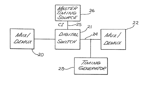
The present invention is illustrated in block diagram in Figure 2. A
multiplexer/demultiplexer 20 is coupled through a digital switching device
21 to a second multiplexer,~demultiplexer 22. In actuality, the plurality of
1~ multiplexers may be joined as part of a network and connected through one
or more digital switches. Clock input 25 is a reference doclc signal from
master timing source 26 and is provided to digital switch 21. This clock
input signal 25 is tapped by a timing generator circuit 23 so that a proper
cloeking signal may be provided to multiplexer 22.
~a
The clock input signal 25 has a phase and frequency component. The
~requency component is required for intersite communication. That is,
~r~qllency synchronization is necessary for communication between the
v~arious sites of the network.
The phase component of the clock input signal 25 is required for
intrasite communication, that is, communication between various phase
dependent devices within each site. The timing generator circuit 23 may
^ receive phase and frequency information and output phase and frequency
11
'
~L 3 ~ ~3 r~
lZ
information. In a second application, the timing generator circuit 23
receives only frequency information and generates phase information for
each site.
The preferred embodiment of the present invention is illustrated in
~igure 3. A pair of clock input cards 56 and 57 each receive a composite clock
signal 38 and a DS1 input signal 39. The outputs 58 and 59 of the input cards
5~ and 57 respectively are coupled to a stratum three clock card 60 and to a
plurality of timing output cards. The present invention operates from
either the composite clock input 38 or the DS1 input 39. Certain of the
timing output cards, such as card 61, provide composite clock output and the
remainder, such as card 62, provide DS1 output. The stratum three card 60 is
pl~.lse locked to the input signal selected and provides its own output 63 to
the timing output cards. 'l`he present invention "reclocks" the input timing
15 signal instead of simply amplifying and repeating it, substantially
~liminating phase delay through the circuit. ~ unique cable compensation
circuit provides negative phase delay for extended window cable runs.
A clock input card is shown in detail in Figure 6. The composite clock
input signal 38 is coupled through transformer 65 to mux 63 and the DS1
in~ut signal 39 is coupled through transformer 66 to mux 64. Mux 64
includes franling logic 67 to capture the frame (phase) information 68 from
tlle DS1 input~ The outputs 69 and 70 of mux's 63 and 64 are coupled to
pllnse lncl;ed loops 71 and 72 respectively. Select logic 73 controls switch 74
to select one of the phase locked loops 71 and 72 to couple to the output
control driver~
Switch 74 is coupled to mux 75 whose output is coupled to mux 76
and mux 77~ The outputs of mux 76 and mux 77 are coupled to Bus A and
13 ~ 3 1 ~
Bus B respectively. Bus A and Bus B are coupled to the stratum three card 60
and to the timing output cards of the timing circuit of the present invention.
.~ source control card 78 is coupled to mux 75 and selects the other timing
input card if the currently "active" card fails.
The stratum three card 60 provides an alternate set of timing signals
on the main bus for the timing output cards. Each timing output card
contains signal select logic to select the timing input signal from the internalinput of the highest priority. The stratum three card 60 includes a clock
la hoklover circuit such as is described in copending patent application
number 131,1~1 filed December 10,1987, entitled CLOCK HOLDOVER
~IRCUIT and assigned to the assignee of the present invention.
The composite clock ~utput card 61 is illustrated in detail in Figure 7.
1~ A select logic block 79 is coupled to the outputs 58 and 59 from the clock
input cards 56 and 57 respectively and to the output 63 of the stratum three
card 60. The select logic block 79 selects one of the three inputs and provides
it as output to the cable phase compensation circuit 80. The cable
eompensation circuit 80 reconstitutes the internal timing signal with an
~a a~ditional delay applied to its output signal 81. The delay is one frame
width plus a negative phase delay equivalent to cable runs of 0-1500 feet in
~ao foot increments. Thus, the output timing signal from a composite clock
aul~ut carcl can drive external timed devices located up to 3000 feet from the
~resent invention~ The window of the cable compensation circuit 80 is
cantrolleel by signals 97 and 98 of control block 96. The control block 96 may
be a pair of switches used to define four windows of cable transmission
length~
13
~ 3 ~
14
The output 81 of the cable compensation circuit 80 is provided to a
composite clock generator 8~ to generate the output composite clock sign~l
83~ The reconstituted and delayed composite clock timing signal 83 is
applieà to eadl port driver through one of the plurality of impedance
5 n~atclling transformers. In the preferred embodiment, a composite clock
timing output card port can drive up to six external devices and each output
card contains up to ten ports. The composite clock output signal is
illustrated in Figure 1.
la A DSl timing OUtp~lt card is illustrated in Figure 8. A priority selector
s~ ts one of the three inputs and provides an output 86 to phase detector
~7~ Pl~ase detector 87 provides an output 55 to a crystal based voltage
~ontrolled oscillator (VCO) 88. The output 93 of VCO 88 is coupled to
divider 89. The divider 89 is coupled in a feedback loop 90 to phase detector
15 B~. The output of divider 8~ is coupled to frame generator 91, which
~enerates a framing signal 92 in either D4 or ES~ mode depending on the
position of switch 94. The output 93 of divider 89 and frame generator 91 is
c~llpled to the DS1 output card ports 95.
The cable compensation circuit of the present invention is illustrated
in ~igure 5~ A clock input signal 49 from select logic 79 is provided as clock
input to shift register 48~ The shift register 48 has a plurality of taps with taps
51-5~ collpleà to a selector 41~ Selector 41 is used to select the arnount of
~has~ ~@lay introduced to the timing signal~ The amount of phase delay
~etermines tlle transmission length window of the present invention. In
th@ ~r~rred embodiment of the present invention, tap 54 represents a full
360 phase delay of the input signal. Each prior tap 51-53 represents
advances in phase of one clock period each.
14
1 3 ~
S~vitches 42 and 43 control which of taps 51-54 of shift re~ister 48 is
selected One terminal of switches 42 and 43 is coupled to ground. Tlle
remaining tap of switch 42 is coupled, at node 45, to the "A" input of selector
41 and through resistor 47 to a 5 volt supply voltage. The remaining
5 terminal of switch 43 is coupled at node 46 to the "B" input of selector 41 and
through resistor 48 to the supply voltage.
In the preferred embodiment of the present invention, tap 54 is
selected when both switch 42 and 43 is open. When switch 42 only is close~l,
10 tap 53 is selected. When switch 43 only is closed, tap 52 is selected and when
both switches are closed, tap 51 is selected. Switches d~2 and 43 allow a user of
the present invention to select both the amount of phase delay and
ultimately, the transmission length window of the input signal.
The output 55 of shift register 48 provides frequency (bit) information
to the composite clock generator 8~ (see Figure 7)~ The output 56 of selector
41 represents phase information of the input signal after having undergone
the desired arnount of delay~
2~ The zero phase delay of the compensation circuit of the present
invention means that the circuit itself disappears for purposes of cable
length calculation~ By advancing phase delay, new length windows can be
defined~ The phase delay is advanced by selecting different taps on the shift
register, where each tap is one clock time (in the preferred embodiment,
~5 1~0~ MHz)~ Each clock time is equal to a 500 foot cable increase~ The timing
length windows in the preferred embodiment are as follows-
- 0 < cable length < 1500 feet
50Q < cable length < 2000 feet
~ 3 ~
16
1000 ~ cable length < 2500 feet
1500 < cable length < 3000 feet
The maximum distance between the timing circuit of the present
S invention and timed devices receiving clocking signals from the present
invention is a function of the data rate. In the preferred embodiment, this
distance is a nominal 1500 feet. If the data rate is higher, the distance is less.
If the data ra~e is lo~ver, the distance is greater.
11~ Thus, a compensation circuit which allows increased transmission
len~ths in a DS0 digital data transfer format is described.
16