Note: Descriptions are shown in the official language in which they were submitted.
1311~1~4
1 --
This invention relates to two-pin electromagnetic flasher
switches which can be utilized in automotive applications.
Flasher switches of various designs have been made in the
past each of which have certain inherent disadvantages.
Thermal flasher switches incorporating a bi-metal
construction designed to be activated upon resistance
heating and expansion of metal components continue to be
in freguent use. Such units are popular due to relatively
low cost of manufacture. Other disadvantages such as
temperature sensitivity and limited lifespan make thermal
switches less favourable in a wide variety of heavy duty
applications such as in trucks. Other flasher switches of
the electro-mechanical type, including the switch
disclosed in U.S. Patent No. 3,611,288, incorporate a
number of moving parts, are generally heavy and are
relatively costly to manufacture and suffer from other
disadvantages.
Flasher switches of known design incorporating single
throw relays have generally been of two basic designs,
that is, having either a two-pin or three-pin
~k
131~
configuration. Similarly, such flasher switches have been
designed for operation under either fixed load or variable
load conditions. These known flasher switches were not
suitable for or capable of being readily adapted for use
in such differing applications without substantially
adversely affecting cost and size considerations.
Flasher switch designs of the two pin type are commonly
used in heavy duty applications in heavy transportation
and construction vehicles such as trucks. Many original
equipment manufacturers (OEM's) have specified flasher
switches of the two-pin type. On the otherhand, although
many passenger car OEM's have featured three pin flasher
switches, there is a demand for two pin flashers which may
be used for after market replacement of failed original
equipment of the three-pin type.
Flasher switches designed for fixed load applications,
particularly for use in connection with turn signal
circuits, when used in connection with multiple lamps,
typically indicate an outage by maintaining the circuit in
the closed position and continuously lighting all
remaining operative lamps. In passenger cars for e~ample,
upon failure of one or more turn signal lamps, there is a
lowering of the load on the flasher switch circuit which
- 3 ~
prevents the relay component of the flasher switch from
being activated to commence flashing of the remaining turn
signal lamps.
Variable load flasher switches are commonly used in hazard
warning light circuits in passenger car motor vehicles and
heavy trucks. Generally, it is essential that hazard
warning lights be capable of operation even if one or more
lamps operated on the circuit have failed. Similarly,
manufacturers and operators of heavy-duty vehicles such as
trucks commonly specify variable load flashing switches
which are capable of operating turn signals even where one
or more lamps are inoperative without significantly
adversely affecting the flashing or cycling frequency of
the remaining lamps. In applications involving trucks, it
is not uncommon for as many as 16 lamps to be operated on
each of both turn signal circuits.
Other design parameters for flashers are typically
specified by OEM's and those parameters are indeed
important in the selection of suitable flasher switches to
meet those requirements. One such parameter is the
maximum elapsed time of operation of the switch f rom
activation to the time of the first flash of the lamps in
operation. It is generally desirable that the f lasher
1 3 ~
switch exhibit a relatively low elapsed time to the first
flash to increase visibility under high speed operation on
highways and the like. A second irnportant parameter is
the frequency of flashing which also must be maintained
within a specified range. Frequencies which are either
too low or too high make the flasher switches undesirable
for use. A third factor is the percentage of time on
during duty cycle which is a measure of the time that the
lamps remain lighted during a full cycle. Other important
design parameters are the durability of the switches,
including the number of cycles expected under normal
operating conditions and resistance to shock and dirt
damage.
The audibility of a flasher switch during operation is
also a relatively important design parameter. Operators
of noisy, heavy equipment, and passenger cars, find it
desirable if the flasher switch generates a relatively
loud noise sufficient to be audible over a range of wind
noise, engine and other noises encountered during vehicle
operation.
Flashers developed for after-market installation in older
vehicles have typically incorporated 2 pin
1 3 ~
-- 5 --
configurations. Flasher assembles of the 3 pin type could
not be readily installed in such older vehicles without
first making modifications to other existing vehicle
components.
In the prior art, electronic flashers have heretofore
incorporated 3 pin configurations, the third pin being a
ground pin. According to the present invention, a two pin
electronic flasher assembly is provided which may be
readily incorporated into new, original vehicle
applications and into after market installations.
Electronic flashers of the present invention may be
adapted to fit existing receptacles having 2 pin or 3 pin
flasher configurations as the need for a third ground pin
has been eliminated.
According to the present invention, it is possible to
provide a reliable electronic flasher switch assembly
manufactured from standardized components at relatively
low cost. The flasher described herein may be
manufactured for use in different applications and using
fewer components to overcome disadvantages associated with
flasher switches of known design.
It is a further aspect of the present invention that the
above described circuit may be r0adily adapted to provide
~ 3 ~
a compact, resilient and durable flasher switch suitable
for heavy duty use in automotive vehicles.
Specific Pmbodiments of the present invention will be
described with reference to the following drawings.
Figure 1 is a schematic drawing of a variable load
flasher switch circuit.
Figure 2 shows various components of a flasher switch
assembly of the present invention.
Figure 3 illustrates a typical printed circuit board
for use in a flasher switch.
With reference to Fig. 1, a diagramatic representation of
one embodiment of the present invention is shown. The
circuit diagram for a two-pin flasher switch shows a
positive source or connection B and a lamp load L.
Positive source B may be connected to the positive
terminal of an automotive battery source (not shown). It
is to be understood that in accordance with the present
invention, switching means (not shown) will be present
intermediate of the load L and the flasher switch circuit,
and that such switching means may include switches of the
3 ~
4-way hazard warning light type or of the directional turn
signal type as will be further described below.
The lamp load L will vary according to the number and
types of operative automotive lamps connected in the
installed circuit. It has been found that using
embodiments of the present invention, it has been possible
to satisfactorily operate sixteen running light lamps on
one flasher circuit at one time. In addition to to other
advantages, it has been found that the operating life of
the present flasher switch is substantially longer than
that of conventional switches.
With reference to Fig. 1, positive source B is connected
to a relatively low resistance shunt 10. Shunt 10 is
connected to both a relay contact 18 and a terminal 7 on
an integrated chip 20. Integrated chip 20 may be of a
type readily available to the automotive parts
manufacturing industry, such as model number UAA 1041
manufactured by Motorola Semiconductor Products Division
of Motorola Limited. As described herein, chip 20 may be
of a type providing overvoltage protection, fault
detection and other protective features. Terminal 7 is a
fault detector pin for detection of, for example, a
shorted lamp socket. If a shorted lamp socket is present
1 3 1 ~
in the circuit a lower voltage is sensed at this terminal
and the signal switch operation is prevented. Terminal
pin 6 acts as an on-off switch for the fault detector
feature. Where, as shown, terminal 6 is not connected to
a positive voltage source, the fault detector feature is
in the on-position. Where this feature is not desired,
the terminal pin 6 should be connected to a positive
voltage source. It is noted that any connection of
terminal 6 to ground (negative) will result in the
virtually immediate destruction of the chip. It is to be
understood that such a feature is possible with fixed load
flasher switches where a unit will be designed to operate
only when all of a specified number of lamps are
functional. In applications where a variable load flasher
switch is desirable, such a fault detection feature is not
possible as it is inherently required that all remaining
functional lamps be permitted to flash upon activation of
the switch. Positive source B is connected to positive
terminal 2 on the chip 20 and source B is further
connected to three capacitors 22, 24, 26 of differing
sizes. In a preferred embodiment capacitors 22, 24 are
rated at 2000 and 1000 uf (microfarads) respectively with
capacitor 26 being rated at 1 uf. It has been found to be
preferential to use two smaller rated capacitors 22, 24
although it is to be understood that a single, larger
~ 3 1 ~
g
capacitor may also be utilized. Where it is desirable to
do so, it is generally found that 2 smaller capacitors can
be so positioned as to reduce the overall size of the
flasher switch device.
Capacitor 22 is connected pin 2 and to diode 32 which
diode acts to suppress discharge of capacitor 22 across
the lighting circuit, namely, the load L. Diode 32 is
connected to resistor 11 which is in turn connected to
sensing terminal pin 8 on the chip 20. Pin 8 acts as a
sensor for detection of the closure of relay contact 18
through detection of a voltage across resistor 11. Diode
30 serves a similar purpose by acting as a gate to
suppress discharge of capacitor 24 across the lighting
circuit. Relay coil 40 is in turn connected to a
corresponding terminal pin 3 on chip 20. Relay coil 40
c~operates with other components of a relay, including an
armature 48 connected to relay contact 18. As may be
readily understood, and as described further below, upon
induction of a magnetic field about relay coil 40,
armature 48 is activated through magnetic attraction
thereby closing the relay contact 18. As shown, capacitor
ser,'es
24 is connected in parallel to suppressor diode 30 as
previously described and to a resistor 13. Resistor 13 is
in turn connected to terminal 1 on chip 20, terminal 1
being the ground or negative contact pin for the chip 20.
-- 10 --
Capacitor 26, which in conjunction with resistor 12
functions as a timer circuit, is connected in parallel to
terminal pin 4 and resistor 12 which resistor is in turn
connected to terminal pin 5 of the chip 20. The f lash
rate of the flasher switch circuit is a function of the
features of the capacitor 26 and resistor 12. The
capacitance rating of the capacitor 26 determines the time
off of lights operating on the flasher circuit and the
corresponding resistance rating of resistor 12 determines
the on time of such lights. It has been found that a very
substantial improvement in flasher switch operation is
experienced when capacitor 26 is selected within a range
of 1 uf to 4.7 uf for corresponding resistances of 430
kohms to 200 kohms in resistor 12.
The operation of the f lasher switch assembly through a
complete cycle may be described in generalized terms as
follows. With reference to Fig. 2, and Fig. 1, upon
activation of a switch such as a directional turn signal
switch or a hazard warning light switch (not shown), a
voltage is sensed at sensing pin 8. Timing capacitor 26
is charged and once charged to capacity, relay coil 40 is
energized, inducing a magnetic field to activate armature
48, thereby closing contact 18. Upon closing contact 18,
reversal in polarity is sensed at terminal 8 causing the
capacitor 26 to discharge. Upon discharge of the
capacitor, the drop out of relay voltage sensed at
terminal 4 continues until the relay contact is again
opened~ To provide a variable load flasher switch,
modifications to the flasher circuit must be made. With
reference to Figure 1, resistor 10 must be a relatively
low resistance connector, commonly known in the art as a
jumper. With a variable load flasher, it is not possible
to utilize any overload protection provided in integrated
chips as it is not possible to specify the number of
lights that may not be operative at any time. However, it
can be appreciated that it is relatively simple to
substitute a jumper for a shunt in a manufacturing process
thereby simplifying any changeovers during production runs.
In the embodiment of the present invention shown in
Fig. 2, it is possible to utilize a printed circuit board
90 of a readily available type as shown in Fig. 3. Fig. 2
shows such a typical circuit board with various of the
pre-drilled bores being labelled according to the
corresponding component to be housed in each such bore.
It should be noted that in Fig. 2, pin 6 of chip 20 is
shown as being connected to a positive source thereby
inactivating the fault detection feature.
- 12 -
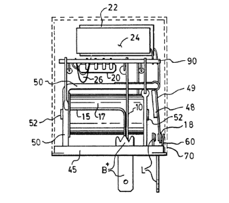
In the assembly of the various components of the flasher
switch device as shown in Fig. 3, it may be desirable to
assemble the relay component by mounting the relay
component on a base 45 of suitable material such as
plastic. The relay will typically include a wound coil
secured about a magnetizable core 52, the core 52 and coil
17 being secured in conductive yoke 50. The base 45
securely holds two pins, a positive terminal B+ and a
ground terminal L for the overall assembly. The armature
48 may be mounted by means of a conductive spring 4g
fastened on the yoke and at its far end supports a contact
18 for corresponding engagement with the ground pin L.
A conductive member such as a shunt 10 is fastened to the
positive pin B+ and is also fastened to the circuit board
90 by soldering or other suitable means. The resistance
of the shunt predetermines the lamp load which may be
operated by the flasher switch and it is thereby possible
to have a fixed load flasher with a shunt of predetermined
resistance or a variable load flasher with a conductive
member of nominal resistance. A conductive connector 15
is also used to electrically connect terminal B+ to the
yoke 50. The shunt also acts as one of several supports
for the circuit board assembly component. The circuit
board assembly may be assembled in a series of steps prior
~3~3~
- 13 -
to its connection to the relay and base assembly. The
chip 20, diodes, resistors and capacitor 26 may all be
soldered or Qtherwise secured into place prior to assembly
with the relay and base assembly. It is expected that the
circuit board assembly may be substantially completed
except to the e~tent that the one or two larger capacitors
22 and 24 may be mounted after the relay and base assembly
is connected to the remainder of the circuit board
assembly. Once those steps are complete, the larger
capacitors may be mounted into place by soldering, for
example. It has been found that desirable characteristics
are achieved when the larger capacitors are mounted on a
first, upper side of the circuit board, and the remaining
components including the remaining timing capacitor, chip,
resistors and diodes are mounted on the second, lower side
of the circuit board intermediate of the circuit board and
relay-base assembly. Ease of manufacturing and space
saving advantages have been recognized as a result of such
component orientations.
The flasher switch assembly of the present invention
provides a further advantage over conventional flasher
switches in that the circuit provides for current loading
through the relay itself rather than the circuit board.
This provides for an improved current loading capacity in
- 14 -
that the entire assembly of the present invention is not
as greatly limited by the typically lower circuit board
capacity. Flasher switches of conventional design have,
for space saving and other reasons, mounted the relay
component on the circuit board such that the circuit board
componentry must carry current loadings between the
terminal pins supported in the base. That is, such
earlier designs have provided for circuit board
componentry to be intermediate of the relay components and
the terminals of the base. Heavy current loadings on such
designs have resulted in premature failure of flasher
switches under moderate loadings. However, flasher switch
assemblies of the present invention, utilizing 40 ampere
rated relay components have satisfactorily serviced 16
truck lights on one turn signal circuit.
In a preferred embodiment of the present invention, an
audible signal indicator may be added to improve driver
detection of flasher operation. In a first embodiment as
shown in Fig. 2, a reverse bent back stop 60 may be angled
to form a slight gap between its distal end and the outer
protective casing or enclosure of the assembled flasher
switch. Upon cycling of the relay, the relay contact will
alternate between contacting the load terminal of the base
and the extended portion of the backstop. Upon impact of
~ 3 ~
the contact with the deflectable number or backstop,
deflection will occur causing the reverse bent portion to
strike the protective casing 70. For example, when the
reverse bent backstop is made of a metallic material and
the casing of a resilient plastic, it is found that
audible turn signal indication characteristics are
enhanced. Alternatively, in yet another embodiment (not
shown), a piezo-electric buzzer or noise maker may be
added to the circuit board to be activated upon cycling of
the flasher circuit. It is understood that other suitable
locations may be found for placement of the buzzer.
Although specific examples and preferred embodiments have
~een expressly disclosed herein, it is understood tht
other embodiments and variations may be utilized without
departing from the scope of the present invention.
2827b/2-16
., .
,