Note: Descriptions are shown in the official language in which they were submitted.
03~
,
POLAR~ZATION I~DEPENDENT
OPTICAL AMPLIFIER APPARATUS
_c~round of the Invention
This invention relates to optical amplifiers and, more particularly, to
S such amplifiers in which the gain differs depending on whether the
electromagnetic mode (i.e., polarization~ of the radiation being amplified is
transverse electric (TE) or transverse magnetic (TM). Included in this class of
amplifiers are semiconductor optical amplifiers in which the radiation is guided in
a waveguide having an asymmetric cross-section.
A major obstacle for the utilization of serniconductor optical
amplifiers in lightwave communication systems is the polarization dependence of
the opfical gain. Typically, the difference in gain between the TE and TM modes
- is several dB. In the laboratory, the polarization can be easily controlled by
twisting bulky fiber loops in the light path so that only one mode (TE) enters the
15 amplifier. In the field, however, lightwave systems must operate unattended for
Iong periods of time and twisted fiber loops are not practical; either active
polarization controllers or polarization independent amplifiers are required.
Because of the added complexity and cost associated with active polarization
controllers, a polarization independent amplifier is the preferred approach.
One proposal for achieving polarization independence is to use two
semiconductor amplifiers in parallel, one for each polarization. As described byG. Grobkopf et al, Electron Lett., Vol. 23, p. 1387 (1987), the input radiation,which is composed of both TE and TM modes, is split into two paths, separately
amplified, and then recombined. However, because of the added complexity of
25 having two optical amplifiers and two couplers, it would be advantageous to have
a scheme that requires only one amplifier and one coupler.
Summary of the Invention
In accordance with one aspect of the invention, which is called a
Polarization Independent Configuration Optical (PICO) amplifier apparatus, a
30 polarization dependent amplifier is used in a double-pass configuration so that any
input radiation will be amplified by an amount approximately equal to the average
of the gains for the TE and TM modes. In one embodiment, the radiation output
of the polarization dependent amplifier has its polarization rotated by essentially
- 90, so that the TE and TM modes are interchanged, before it is re-amplified by
35 the same polarization dependent amplifier. The gain disparity between the twomodes is thereby greatly reduced (e.g.~ from 4 dB to 0.2 dB, a factor of 20 in dB),
~ 13110~
and essentially polarization independent amplihcation is achieved.
Tn accordance with one aspect of the invention there is provided optical
amplifier apparatus independent of the polarization of the optical radiation to be
amplified comprising an optical amplifier which has different gain for l'E and TM modes
S of said of optical radiation, means for transmitting both polarizations of said radiation
through said amplifier, and characterized by means located external to any resonator for
rotating both of said polarizations of said radiation by n90, where n is an odd integer,
after it emanates from said amplifier and for transmitting said polarization-rotated
radiation through said amplifier again so that the gains of said TE and TM modes passing
10 through said ampliFler an even number of times are essentially equal.
Brief Dcscription of the DrawinY
The invention, together with its various features and advantages, can be readilyunderstood from the following more detailed description taken in conjunction with
accompanying drawings, in which:
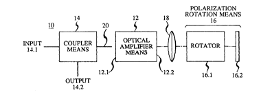
FIG. 1 is a schematic, block diagrammatic view of a PICO amplifier apparatus
in accordance with one embodiment of the invention; and
FIG. 2 is a graph Gf optical gain for the input polarization giving the highest
gain (curves I and III) and lowest gain (curves II and IV) in a PICO ampli~ler apparatus
(curves III and IV), and in a conventional amplifier (curves I and II) in a double-pass
20 configuration.
Detailed DescriPtion
Turning now to FIG. 1, there is shown PICO amplifier apparatus 10 which
includes a polarization dependent optical amplifier means 12; that is, at least one optical
amplifier which exhibits a difference in gain depending on whether the radiation to be
25 amplified is oscillating in a TE mode or a TM mode. Means 12 could, for example,
include several amplifiers in tandem at least one Oe which has such polarization dependent
gain.
The radiation to be amplified is applied to one end 12.1 of the amplifier means
12 illustratively via an optical coupler means 14 which includes an input port 14.1 and an
30 output port 14.2 for, respectively, applying an input optical signal and extracting an output
optical signal from apparatus lQ.
,f~
1 31 1 038
- 2a-
A significant aspect of the invention is the operation of the polarization
dependent optical amplifier means 12 in a multiple-pass (e.g., double-pass)
configuration in such a way that TE and TM modes passing through the amplifier in
the forward direction are interchanged in the backward direction. Consequently, the
S TE and TM modes experience essentially equal gain, on average, after an even number
(e.g., two) of passes through amplifier means 12.
To ef~ect this interchange of TE and TM modes, the radiation emanating
from the other end 12.2 of amplifier means 12 is passed through polarization rotation
means 16 where its polari%ation is rotated by 90 (or an odd integral multiple
10 thereof) be~ore it passes again through amplifier means 12. In an illustrative
embodiment of the invention, polarization rotation means 16 includes a Faraday
rotator 16.1 (bulk or thin film type) and a reflector or mirror 16.2. Radiation
emanating from end 12.2 of amplifier means 12 is focused by lens means 18 onto
rotator 16.1 which rotates its polarization by 45 in the forward
t ~ 1 1 038
- 3 -
direction. Thereafter, the 45-rotated radiation is reflected by mirror 16.2 back
into rotator 16.1 so that on the second pass therethrough the radiation experiences
another 45 rotation of its polari~ation. The total polari~ation rotation of both the
TM and TE modes is 90, which means that these modes have been interchanged.
From an analytical standpoint, the total gain GTOT(TE) for radiation in
the TE mode will be the product of GTE. the TE mode gain, in the forward
direction, times GTM~ the TM mode gain, in the backward direction because the
TE mode has been rotated by 90 into TM the mode. Thus,
GTOT (TE) = GTE GTM ( I )
10 Conversely, the total gain GTOT(TM) for radiation in the TM mode will be
GTOT(TM) = GTM GTE (2)
Assuming the amplifier to be linear in the range of operation (as ie is for manysemiconductor optical arnplifiers), then
GTM-GTE = GTE'GTM ( )
15 or GTOT(TE) = GTOT(TM) (4)
and both the TM and TE modes experience tlle same gain in apparatus 10
independent of the fact that the GTE and GTM are different in the polarization
dependent amplifier means 12. In practice, there may still be some slight
polarization dependence, but a substantial improvement has been achieved and it
20 is reasonable to characterize the apparatus as essentially polarization independent.
In order to achieve the above result, the amplifier means 12 should be
of the non-resonani type; that is, the ends 12.1 and 12.2 should not be highly
reflecting. Thus, where amplifier means 12 is a semiconductor optical amplifier,the end facets of the semiconductor chip should be provided with suitable anti-
25 reflection coatings well known with art. Preferably, the reflectivity R of suchcoatings is very low (e.g., < 10-3) and is related to the gain of the single-pass
amplifier G as follows:
4 t311038
GR < 0.10 (5)
for a gain ripple of about one dB. This condition should be satisfied for both the
TE reflectivity and Ihe TM reflectivity.
Exarnple
S The following example describes PIC(~ amplifier apparatus of the typeshown in FIG. 1, but specific components, materials, device and/or operating
parameters are provided by way of illustration only and, unless otherwise
indicated, are not intended to limit the scope of the invention.
The amplifier means 12 of FIG. 1 was made from a 500 ~m long
10 Channel Substrate Buried Heterostructure (CSBH) laser chip with a quarter
wavelength SiOX anti-reflection coating applied to both facets (ends 12.1 and
12.2). The average l'E facet reflectivity was less than 10~. The input radiationwas coupled to the amplifier chip with a lensed fiber 20 and coupler means 14.
The latter comprised a fiber coupler which separated the input and output signals
15 equally on ports 14.1 and 14.2; i.e., t!lis type of coupler is referred to as a
50/50 fiber coupler. The output from the other end 12.2 of the amplifier chip was
collimated with a 0.85 NA microscope objective (lens means 18) and sent through
a ~:araday rotator 16.1 with a rotation angle of 45. The Faraday rotator was
formed from a well-known 1.5 ~lm optical isolator (a YIG crystal and magnet, but20 with the polarizers removed). After reflection from the high reflectivity
mirror 16.2, the polarization was rotated another 45~ and re-entered the
amplifier chip, but now with orthogonal polarization to the input signal. The input
polarization was adjusted with a well-known fiber polarization controller (not
shown) inserted between coupler means 14 and the amplifier chip.
The gain of the PICO amplifier apparatus was measured by coupling
an amplitude modulated output from a 1.32 ,um DFB laser into the amplifier chip
via coupler input 14.1 and measuring the amplified output signal at coupler
output 14.2 with a high-speed receiver and a RF spectrum analyzer. The DFB
laser was modulated with a 01010... bit sequence at 1.7 GBit/s, and the RF power30 at the 850 M~z fundamental frequency was proportional to the square of the
optical gain. The polarization of the input signal at port 14.1 was adjusted to give
the highest and lowest gain for each measurement point. These measurements
were first made without the Faraday rotator 16.1 in the optical path in order tomeasure the intrinsic polarization dependence of the amplifier chip as shown in
1 3 1 1 038
- 5 -
FIG. 2 (solid line curves I and 11). The gain for the TE mode (curve 1) is shownto be abollt 4 dB higher than the gain for the TM mode (culve II). However,
when the Faraday rotator 16.1 was inserted and the same measurements were
repeated, the datapoints corresponding to the dashed lines (curves III and IV) were
5 obtained. The gain difference between the TE and TM modes was reduced about
0.2 dB. Also note ~hat the gain with the Faraday rotator in place is the average(in dB's) of the "best" and "worst" gain without the Faraday rotator. At 40 mA of
amplifier current, the net fiber-to-fiber amplifier gain (not counting losses in the
coupler 14) was 9 dB and single-pass gain was estimated to be about 13 dB.
In the PICO amplifier apparatus, where the input and output optical
radiation share a common path through amplifier means 12 and rotation means 16,
the input and output signals must be separated. In this experiment, coupler
means 14 was a 50/50 fiber coupler which gave an excess coupling loss of 6 dB.
This excess loss, however, can be reduced. If coupling means 14 comprises a
15 well-known polarization independent optical circulator, the two signals can be
separated without substantial excess loss. Such a circulator is described by
W. L. Emkey, IEEE J. Li~htwave Technolo~y, Vol. LT-1, pp. 466-469 (1983).
It is to be understood thàt the above-described arrangements are
merely illustrative of the many possible specific embodin ents which can be
20 devised to represent application of the principles of the invention. Numerous and
varied other arrangements can be devised in accordance with these principles by
those skilled in the art without departing from the spirit and scope of the
nvention.