Note: Descriptions are shown in the official language in which they were submitted.
131 1052
The present invention relates to a ~eedback
control apparatus in an optical recording and reproducing
device for recording, reproducing and/or erasing data with
use of a recording medium by projecting a light beam
thereto, which controls the illuminating conditions of the
light beam projected onto the recording medium.
Optical recording and reproducing devices for
recording and/or reproducing data with use of an optical
recording medium by projecting a light beam thereto such as
optical disk devices, optical card devices, and the like can
perform high density recording since the diameter of a bit
which is a recording unit of data can be easily arranged to
about 1 ~m. Thanks to this advantage, the above type of
recording and reproducing device has been in a spotlight in
recent years as a recording device capable of recording a
great amount of information.
In order to constantly perform such high density
recording with a bit having a diameter of approximately 1
~m, a tolerance of the order of submicron is required on the
diameter of the bit, and focusing control and positioning
control of the light beam or the like at the time of
recording and reproducing of data.
Therefore, generally provided in optical recording
and reproducing devices are feedback control apparatuses for
executing control loops, the apparatuses comprising an
actuator for controlling the illuminating conditions such as
the focusing condition and illuminating position of a light
beam projected onto a recording medium, a detection unit for
detecting the aforementioned illuminating conditions, and a
control amplifier for driving the actuator in accordance
with an output signal from the detection unit.
The signal level of a detection signal output from
the detection unit becomes 0 for example when the
illuminating conditions of the light beam projected onto the
recording medium are appropriate. Therefore, if a control
amplifier having high accuracy in amplifying and
1 ~ 1 1 052
compensating operation is adopted as the control amplifier,
it will be ensured that the signal level of the control
signal released from the control amplifier becomes 0 thereby
keeping the actuator in a stationary state.
In contrast, when an operational amplifier for
general purpose is used as the operational amplifier, a DC
offset is likely to be generated in the output signal from
the control amplifier due to a minute offset in the output
of the operational amplifier caused by the characteristics
of the operational amplifier itself, slight fluctuation in
the power voltage applied to the operational amplifier, etc.
Such a DC offset tends to increase still more when
increasing the overall gain of the control loop and the gain
of the individual circuits which form the control amplifier
in order to improve the response of the control loop and
accuracy in the follow-up system thereof.
Therefore, even though the signal level of the
detection signal released from the detection unit is 0, the
signal level of the control signal from the control
amplifier does not necessarily become 0. This results in
the flow of current into the actuator causing the actuator
to be driven, leading to positional errors.
In practice, these positional errors increase
since the DC offset increases in proportion to the increase
in the overall gain of the control loop.
Further, when the DC offset increases, the output
of the phase lag circuit and amplification circuit which
have high-gain low frequency components approach the
saturation level. As a result, the control loop is not
executed optimally and subsequent control over the
illuminating conditions of the optical beam projected onto
the recording medium is lost.
To solve the above problem, some conventional
feedback apparatuses are designed such that an offset
compensation signal is entered in the subtraction circuit to
execute a differential input, the subtraction circuit being
13~ 1052
located before the phase lead circuit, phase lag circuit,
and amplification circuit which have high gain, and the
signal level sf the offset compensation signal is adjusted
to a desired level by a variable resistor.
In such prior art apparatuses, a DC offset caused
by a minute offset in the output of the operational
amplifier slight fluctuation in the power vol~age or the
like, is cancelled by the offset compensation signal. For
example, when the signal level of the detection signal from
the detection unit is 0, the signal level of the control
signal released from the control amplifier is controlled to
be 0 thereby reducing positional errors.
Such a minute offset in the output signal of the
operational amplifier and fluctuation in the power voltage,
however, vary depending on operational amplifiers and power
units. Therefore, conventionally, every feedback control
apparatus in an optical recording and reproducing device is
required to be adjusted in the manufacturing process in
order to prevent the occurrence of DC offsets. This
additional adjusting process results in increased production
costs.
Furthermore, if the power condition or the
environment where the apparatus is used changes after the
adjustment has been made, a minute offset will be generated
in the output signal of the operational amplifier and the
power voltage will fluctuate. This makes it difficult to
positively prevent the increase of DC offsets and an
abnormal control operation.
It is naturally possible to employ an operational
amplifier of high accuracy and a power unit having a high
stability in order to prevent the occurrence of DC offsets,
but this also brings about a considerable increase in the
production cost.
An object of the present invention is to provide
a feedback apparatus in an optical recording and reproducing
device, which is capable of actively preventing a DC offset
1 31 1 052
in the control signal released from the control amplifier,
thereby minimizing the adjusting processes in man~facturing
without the use of e~pensive parts, or devices and resulting
in a reduced production cost saving.
In order to achieve the foregoing, the present
invention provides a feedbac~ control apparatus in an
optical recording and reproducing device for recording,
reproducing and/or erasing data with use of an optical
recording medium by projecting a light beam emitted from an
optical head onto the optical recording medium, which device
comprises an actuator for controlling the illuminating
conditions of the light beam projected onto the optical
recording medium, a detection unit for detecting the
illuminating conditions of the light beam projected onto the
optical recording medium, a control amplifier for driving
the actuator in accordance with a detection signal released
from the detection unit, thereby controlling the
illuminating conditions of the light beam projected onto the
recording medium, is characterized by switching means for
selectively switching from a detection signal released from
the detection unit to a reference signal, or vice versa, for
entering in the control amplifier, the reference signal
having the same signal level as that of a detection signal
which is expected to be released from the detection unit
when the illuminating conditions of the light beam projected
onto the recording medium are appropriate; and offset
compensation means for releasing an offset compensation
signal to the control amplifier, the offset compensation
signal being set such that a control signal generated in the
control amplifier has a predetermined signal level when the
reference signal is entered in the control amplifier.
The offset compensation means may include an ~/D
convertor for converting an analog signal from the control
amplifier into a digital signal; a CPU for releasing a
digital signal for compensating for an offset in the control
amplifier in accordance with the digital signal from the A/D
131 1052
converter; and a D/A converter for converting the digital
signal from the CPU into an analog signal thereby releasing
an offset compensation signal to the control amplifier.
The D/A converter may be designed so as to
maintain the level of the offset compensation signal
released in accordance with the digital signal from the CPU
even after the CPU stops the output of digital signals.
Th4 offset compensation means may be designed so
as to change the signal level of the offset compensation
signal by fixed values until it reaches a predetermined
level in case the control signal released from the control
amplifier when the reference signal is entered in the
control amplifier has not the predetermined signal level.
Further, the offset compensation means may be
designed so as to delay the output of the offset
compensation signal which is executed in accordance with the
signal level of the output signal from the control amplifier
by a corresponding time period to the response time of the
control amplifier.
Further, the offset compensation means may be
designed so as to execute offset compensation at the time
when activating of the feedback control apparatus in the
optical recording and reproducing device is initiated.
Still further, the offset compensation means may
be designed so as to execute offset compensation at the time
when resetting of the feedback control appar~tus in the
optical recording and reproducing device is executed.
Embodiments of the invention will now be
described, by way of example, with reference to the
accompanying drawings, in which:
Figure 1 is a circuit diagram showing the
construction of a conventional control amplifier;
Figure 2 is a block diagram showing the
construction of a control unit disposed in a feedback
apparatus in an optical recording and reproducing device of
the present invention;
1 3 1 1 052
Figuxe 3 is a block diagram showing the
construction of the feedback control apparatus; and
Figure 4 is a flow chart describing the operations
executed by a CPU in an offset compensating means.
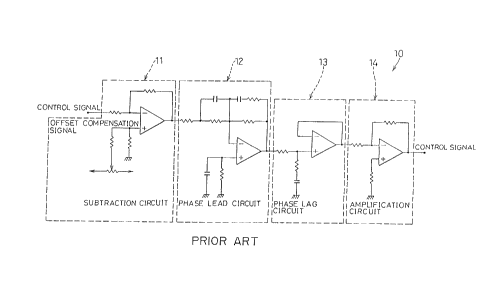
Referring to Figure 1, the control amplifier 10
which is a component of the feedback control apparatus
comprises a subtraction circuit 11, a phase lead circuit 12,
a phase lag circuit 13 and an amplification circuit 14. In
the subtraction circuit 11, an output signal from the
detection unit in accord with the illuminating conditions of
a light beam projected onto the recording medium, and an
offset compensation signal are entered to obtain the
difference. In the phase lead circuit 12, a phase lag
caused by the current-displacement conversion characteristic
of the actuator in a high frequency region is electrically
compensated so as to obtain a phase margin in the vicinity
of the cut-off frequencies of the control loop thereby
preventing the control loop from being unstableO
The phase lag circuit 13, functions to increase
the loop gain in a low frequency region, thereby improving
the response of the overall control loop, and controlling
errors in low frequency components caused by errors in
initially setting the individual devices to be actuated by
the actuator. The amplification circuit 14 functions to
amplify the signal which has been compensated at the phase
lead circuit 12 and the phase lag circuit 13, and to release
the signal thus amplified as a control signal for driving
the actuator.
The signal level of a detection signal released
from the detection unit becomes O for example when the
illuminating conditions of the light beam projected onto the
recording medium are appropriate. Therefore, if a control
amplifier having high accuracy in amplifying and
compensating operation is adopted as the control amplifier
10, it will be ensured that the signal level of the control
131 1052
signal released from the control amplifier 10 becomes 0
thereby keeping the actuator in a stationary state.
In contrast, when an operational amplifier for
general purpose is used as the operational amplifier
comprising the phase lead circuit 12, the phase lag circuit
13, the amplification circuit 14 and the like, a DC offset
is likely to be generated in the output signal from the
control amplifier 10 due to a minute offset in the output of
the operational amplifier caused by the characteristics of
the operational amplifier itself, slight fluctuation in the
power voltage applied to the operational amplifier, etc.
Increasing the overall gain of the control loop and the gain
of the individual circuits which comprise the control
amplifier 10, in order to improve the response of the
control loop and the accuracy in the following systems,
tends to increase the DC offset even further.
Therefore, even though the signal level of the
detection signal released from the detection unit is 0, the
signal level of the control signal from the control
amplifier 10 will not necessarily become 0. The result is
a flow of current into the actuator causing the actuator to
be driven.
Positional errors X that can be expected in the
individual devices actuated by the actuator is given
approximately by:
X = Vof X ~X / A
wherein Vof: DC offset in the control signal released from
the control amplifier 10;
~ X: Sensitivity of the actuator i.e., the ratio
of the displacement of the individual devices actuated by
the actuator to voltage to be applied to the actuator;
A- Overall gain of the control loop.
The above positional errors X may prevant the
illuminating conditions of the light beam projected onto the
recording medium from being kept at optimum conditions.
1 31 1 ~5~
It is theoretically expected that the positional
errors ~ will decrease when the overall gain of the control
loop increases, since the positional errors X is inversely
proportional to the overall gain of the control loop.
However, in practice the positional errors X increase since
the DC offset increases in proportion to the increase in the
overall gain of the control loop as mentioned above.
Further, when the DC offset increases, the output
of the phase lag circuit 13 and amplification circuit 14
which have high-gain low frequency components approach to
the saturation level resulting in improper functioning. As
a result, often the control loop is not normally executed
and subsequent control over the illuminating conditions of
the optical beam projected onto the recording medium is
lost.
To solve the above problem, some conventional
feedback apparatus are designed such that an offset
compensation signal is entered in the subtraction circuit 11
to execute a differential input, the subtraction circuit
being located before the phase lead circuit 12, phase lag
circuit 13, and amplification circuit 14 which have high
gain, and the signal level of the offset compensation signal
is adjusted to a desired level by a variable resistor 15.
In such prior art apparatuses, a DC offset caused
by a minute offset in the output of the operational
amplifier or slight fluctuations in the voltage or the like
is cancelled by the offset compensation signal. For
example, when the signal level of the detection signal from
the detection unit is 0, the signal level of the control
signal released from the control amplifier 10 is controlled
to be 0 thereby reducing positional errors.
Such a minute offset in the output signal of the
operational amplifier and fluctuation in the power voltage,
however, vary depending on operational amplifiers and power
units. Therefore, conventionally, every feedback control
apparatus in an optical recording and reproducing device is
1 ~1 1 052
required to be adjusted in the manufacturing process in
order to prevent the occurrence of DC offsets. This
additional ad~usting process results in increased production
costs.
Furthermore, if the power condition or the
environment where the apparatus is used changes after
adjustment has been done, a minute offset will be generated
in the output signal of the operational amplifier and the
voltage will fluctuate. This makes it difficult to
completely prevent the increase of DC offsets and results in
abnormal operation.
Referring now to Figures 2 to 4, an embodiment of
the present invention will be explained in detail
hereinbelow.
There is provided in a recording and reproducing
device for recording, reproducing and/or erasing data with
use of a recording medium 21, an optical head 23 for
projecting a light beam such as laser light or the like onto
the recording medium 21 as shown in Figure 3. The optical
head 23 is provided with a lens 24 for converging light on
the recording surface of the recording medium 21 to form a
light spot; an electro-magnetic actuator 25 for moving the
lens 24 in the direction of an optical axis for example so
as to control the illuminating conditions of the optical
beam projected onto the recording medium 21, i.e., focusing
and positioning of the light beam projected on the recording
medium 21 and the like; a detection unit 26 for detecting
the illuminating conditions of the light beam projected on
the recording medium 21 and releasing a detection signal
based thereon.
As the detection unit 26, a detection system with
use of astigmatism which is popularly used in a reproducing
device for a compact disk, video disk or the like is
employed for detecting a focal error and positional error.
This detection unit 26 is connected to a control
unit 31. The control unit 31 is, as shown in Figure 2,
131 1052
provided with switching means 32 in which a detection signal
from the detection unit 26 is entered. A ground level
signal, that is, a reference signal having the same signal
level as that of a detection signal expected to be released
from the detection unit 26 when the illuminating conditions
of the light beam projected from the optical head 23 onto
the recording medium 21 are appropriate, is entered in the
switching means 32. The switching means 32 has a function
of selectively switching from the detection signal released
from the detection unit 26 to the reference signal, or vice
versa for outputting. The signal thus selected and released
from the switching means 32 is entered in the control
amplifier 33. The control amplifier 33 is designed to
release a control signal for driving the actuator in
accordance with the detection signal when the detection
signal from the detection unit 26 is entered in the control
amplifier 33 via the switching means 32.
The output control signal from the control
amplifier 33 is entered in a driver 41. The control signal
entered in the driver 41 is amplified and then sent to the
electro-magnetic actuator 25 thereby driving the electro-
magnetic actuator 25.
The control amplifier 33 generates a monitor
signal indicating the signal level of the control signal and
sends it to an A/D converter 34 which performs analog-to-
digital conversion. A digital signal released from the A/D
converter 34 is entered in a CPU 35 which controls offset
compensating operation.
A digital signal from the CPU 35 is entered in a
D/A converter 36 which performs digital-to-analog conversion
and an analog signal from the D/A converter 36 is entered in
the control amplifier 33 as an offset compensation signal
the signal level of which is added to or subtracted from
that of the detection signal from the detection unit 26 or
the reference signal. The CPU 35 also generates a switching
1~1 1052
control signal for controlling the switching operation of
the switching means 32.
Offset compensation means 37 is provided to set
the signal level of an offset compensation signal such that
the control signal from the control amplifier 33 has a
predetermined signal level in the case the reference signal
is sent from the switching means 32 into the control
amplifier 33 via the A/D converter 34, the CPU 35 and the
D/A converter 36, and send the above offset compensation
signal to the control amplifier 33.
A feedback control apparatus 22 for controlling
the illuminating conditions of the light beam projected on
the recording medium 21 executes a control loop comprising
the optical head 23, the electro-magnetic actuator 25, the
detection unit 26, the control unit 31 and the driver 41.
The operations performed by the CPU 35 in the
apparatus having the above construction will be explained
hereinbelow with reference to the flow chart of Figure 4.
The offset compensating operation performed by the
offset compensation means 37 is one of the initial
operatiGns which are automatically carried out, for example,
when actuating the recording and reproducing device. This
operation is also carried out when resetting the optical
recording and reproducing device for some purposes.
In the above cases, the CPU 35 firstly releases
the switching signal to the switching means 32 so that the
reference signal of a ground level is entered into the
control amplifier 33 (S1~. Then, an initial value is set in
the D/A converter 36 to enter an offset compensation signal
having a predetermined level in the control amplifier 33
(S2).
Addition or subtraction operation is performed on
the reference signal thus entered using the signal level of
the offset compensation signal as an addend or subtrahend
and the signal obtained from the above operation is
compensated for its phase and amplified so as to be released
1 ~ 1 1 052
from the control amplifier 33 as a control signal. The
control amplifier 33 also releases a monitor signal ~hich
indicates the signal level of the control signal. After
counting the time period corresponding to the response time
of the control amplifier 33 from the input stage to the
output stage (S3), the CPU 35 monitors the digital signal
which has been converted by the A/D converter 34 in
accordance with the monitor signal (S4).
Thereafter, it is judged according to the digital
signal from the A/D converter 34 whether or not the signal
level of the control signal from the control amplifier 33 is
within a predetermined allowable range (S5). More
specifically, since there has been entered in the control
amplifier 33 via the switching means 32, the reference
signal having the same signal level as that of the detection
signal which is expected to be released from the detection
unit 26 when the illuminating conditions of the light beam
projected from the optical head 23 onto the recording medium
21 are appropriate, it can be judged whether a DC offset is
properly cancelled by the offset compensation signal by
means of judging whether the signal level of the control
signal is within e.g. the range of a tolerance.
If it is judged in S5 that the signal level of the
control signal from the control amplifier 33 is not within
a predetermined allowable range, the CPU 35 returns the
program to S2. The CPU 35 again provides in the D/A
converter 36, a value obtained by adding or subtracting a
preset value from the value which has been previously set in
the D/A converter 36, and then repeats the procedures in S3
to S5.
On the other hand, if it is judged in S5 that the
signal level of the control signal from the control
amplifier 33 is within a predetermined allowable range, the
program proceeds to S6 where the switching control signal is
sent to the switching means 32 so that the detection signal
from the detection unit 26 is entered in the control
131 1052
amplifier 33 whereby the control operation over the
illuminating conditions of the light beam projected onto the
recording medium 21 is properly performed.
In this case, the value set by the CPU 35 is kept
in the D/A converter 36 so that the signal level of the
offset compensation signal is maintained so as to properly
cancel a DC offset as described above until the next offset
compensation operation is performed.
For instance, when controlling the focus of the
light beam, if the lens 24 is suitably located with respect
to the recording position on the surface of the recording
medium 21, the amount of the actuating current flowing to
the electro-magnetic actuator 25 becomes 0, so that it is
possible to precisely position the lens 24 to fit to the
irregularities of the recording surface thereby preventing
the occurrence of remaining errors and unstable operations.
In the foregoing embodim~nt, the case where DC
offset compensation is performed on the overall control
amplifier 33 has been explained, but the present invention
is not limited to the above embodiment. For example, such
DC offset compensation may be respectively carried out with
respect to the individual operational amplifiers and control
circuits in the control amplifier 33, and a plurality of
separated units.
As described above, according to the present
invention, the feedback control apparatus in an optical
recording and reproducing device for recording, reproducing
and/or erasing data with use of an optical recording medium
by projecting a light beam emitted from an optical head onto
the optical recording medium, which comprises an actuator
for controlling the illuminating conditions of the light
beam projected onto the optical recording medium, a
detection unit for detecting the illuminating conditions of
the light beam projected onto the optical recording medium,
and a control amplifier for driving the actuator in
accordance with a detection signal released from the
131 1052
14
detection unit, thereby controlling the illuminating
conditions of the light beam projected on the recording
medium, is characterized by:
switching means for selectively switching from a
detection signal released from the detection unit to a
reference signal, or vice versa, for entering in the control
amplifier, said reference signal having the same signal
level as that of a detection signal which is expected to be
released from the detection unit when the illuminating
conditions of the light beam projected onto the recording
medium are appropriate; and
offset compensation means for releasing an offset
compensation signal to the control amplifier, said offset
compensation signal being set such that a control signal
generated in the control amplifier has a predetermined
signal level when the reference signal is entered in the
control amplifier.
The offset compensation means may include an A/D
converter for converting an analog signal from the control
amplifier into a digital signal; a CPU for releasing a
digital signal for compensating for an offset in the control
amplifier in accordance with the digital signal from the A/D
converter; and a D/A converter for converting the digital
signal from the CPU into an analog signal thereby releasing
an offset compensation signal to the control amplifier.
The D/A converter may be designed so as to
maintain the level of the offset compensation signal
released in accordance with the digital signal from the CPU
even after the CPU stops the output of digital signals.
The offset compensation means may be designed so
as to change the signal level of the offset compensation
signal by fixed values until it reaches a predetermined
level in case the control signal released from the control
amplifier when the reference signal is entered in the
control amplifier has not the predetermined signal level.
131 1~5~
Further, the offset compensation means may be
designed so as to delay the output of the offset
compensation signal which is executed in accordance with the
signal level of the output signal from the control ~mplifier
by a corresponding time period to the response time of the
control amplifier.
Further, the offset compensation means may be
designed so as to execute offset compensation at the time
when activating of the feedback control apparatus in the
optical recording and reproducing device is initiated.
Still further, the offset compensation means may
be designed so as to execute offset compensation at the time
when resetting of the feedback control apparatus in the
optical recording and reproducing device is executed.
As described above, the signal level of the offset
compensation signal is set by the offset compensation means
so that the control signal from the control amplifier has a
predetermined signal level when the reference signal is
entered in the control amplifier, said reference signal
having the same signal level as that of a detection signal
which is expected to be generated in the detection unit when
the illuminating conditions of the light beam projected onto
the recording medium are appropriate.
More specifically, since the signal level of the
offset compensation signal is set such that the control
signal from the control amplifier has a predetermined signal
level in the case the illuminating conditions of the light
beam projected onto the recording medium are appropriate,
even if the minute offset in the output signal of the
operational amplifier, the fluctuation in the power voltage
or the like varies depending on operational amplifiers and
power units, it is possible to positively prevent a DC
offset from being included in the control signal from the
control amplifier thereby performing stable data
recording/reproducing/erasing operations on the recording
medium.
131 1052
16
Therefore, without using expensive parts or
devices such as an operational amplifier of high accuracy
and power unit having a high stability, it is possible to
positively prevent a DC offset from being included in the
control signal from the control amplifier. Moreover, there
is no need to adjust the signal level of the offset
compensation signal in every apparatus in the manufacturing
process, and therefore the number of processes required for
adjustment as well as the production cost can be reduced and
the performance of the apparatus can be prevented from
varying.
Even if the power condition or the environment in
which the apparatus is used should change, the signal level
of the offset compensation signal can be set to suit for the
power condition/environment by the offset compensation
means, so that a DC offset can be positively prevented from
being included in the control signal released from the
control amplifier.