Note: Descriptions are shown in the official language in which they were submitted.
131 126~
008-101-3
TITLE: COMPACT FLUORESCENT I~MP CIRCUIT
This invention relates to starting and operating
circuits for use with super compact ~luorescent lamps
and particularly to such circuits which are effective
to start the lamps in cold temperature conditions.
Backqround of the Inventlon
In the recent past, a new form of fluorescent lamp
has been introduced in the market place and is known as
a super compact fluorescent lamp. This type of lamp
differs from the conventional lamp in having a "folded"
kind of construction~ Rather than havin~ connectors at
opposite ends of a tubular envelope, as has been
customary with either the linear lamps or the U-shaped
lamps, the supex compact lamps have a single base which
houses all o~ the electrical connections. In this
respect, the super ~ompact lamps~resemble a more
conventional incandescent lamp and can be used to
replac~ incandescent ànd low wattage~ high intensity
discharge~lamp fixtures in many circumstances.
At the present time, Iamps are available in
various sizes ranging ~rom 10 to about 26 watts, the
lamp havlng an outside length of from about ~ 5 in. to
about 7.5 in. measuring from the tip of the base to the
tip of the glass envelope. These lamps produce light
1 3 1 1 ~0
in the range o~ from about 600 to about 200Q lumens.
The base is a plug-in base and the lamp has two
filaments as do many of the better-known elongated
tubular varieties. As will be recogrlized, the light
output from these lamps makes them suitable for
replacing incandescent lamps having up to about a 150
watt rating.
Although the super compact lamps have many
characteristics in common with the tubular varieties,
it has been found that there are also some significant
operational differences. In particular, it has been
found that the standard starters are not adequate to
start the super compact lamps under low temperature
conditions, particularly below 15F, and that starting
of the lamps was not reliable under a temperature of
35DF. Although the reason for this is not completely
understood, it has been theorized that mercury ions
within the lamp are condensed or ~rozen out of the gas
: because of the greater glass wall area, thereby
increasing the lamp ignition peak voltage to a level at
which the starter repeatedly attempts unsuccessfully to
start th lamp, ultimately resulting in its sel~-
destruction.
Summary bf the Invention
: Accordingly, the prese.nt in~ention seeks
: to provide starter circuits which are usable toef~ectively and reliably start super compact
fluorescent lamps under low temperature environmental
conditions.
As used herein, the expression "low temperature"
is used to re~er to any temperature a~ or below the
~reezing of water, although the circuits dlsclosed
'h
1 3~ 1 26Q
herein have been shown to be effective at temperatures
as low as -65'F.
Briefly described, the invention includes a
starting and operating circuit having a ballast reactor
connectible to a source of line voltage and a super
compact fluorescent lamp having two filaments, one
terminal of each of the filaments being connected
through the reactor to the source. A first circuit
including a pulse transformer and a high frequency
coupling capacitor is provided for furnishing sta:rting
pulses to the lamp, the pulse transformer circuit being
connected to the other terminals of the lamp filaments.
A second circuit, also connected between the other
terminals of the filaments, includes a radio frequency
~RF) choke, a charging resistor and a storage capaaitor
connected in series. A breakdown device is connected
between the storage capacitor and the pulse transformer for
providing a pulse to the transfo~mer in response to the
: development of a trigger voltage on the ~torage
capacitor. A positive temperature coefficient (PTC)
resistor is connected in parallel with the charging
resistor and storage capacitor~ The PTC resistor has a
cold resistance significantly less than that of the
charging resistor and storage capacitor so that when
energy is first supplied to the lamp and starting
circuit and when current flows through the filaments,
the choke and one of the parallel-connected circuits,
substantially more current flows ~hrough the PTC
resistor than through the charging resistor. The PTC
resistor has a warm resistance signi~icantly greater
- than the charging resistor so that when the PTC
resistor and the filaments are warm, currant is
~: diverted into the charglng resistor and storage capacitor,
: charging the storage capacitor to the trigger ~evel and
. " ~ ~
. ~;
131 1260
triggerlng the breakdown device to produce starting
pulses for the lamp.
The invention pertains to a super compact
fluorescent lamp starting and operating circuit
including a ballast connectible to a source of line
voltage, the ballast having a primary portion and a
secondary portion and the secondary portion having a tap
defining a tapped portion at the output end thereof. A
super compact Eluorescent lamp has first and second
fiIaments, one terminal of the first filament being
connected through the ballast to the source and one
terminal of the second filament being connected to the
common line of the source and the ballast. A high
frequency coupling capacitor is connected across the
terminals oE the first filament. Circuit means
including an RF choke and a storage capacitor is
connected in series circuit relationship with each other
between ~he tap on the secondary portion of the ballast
and the other terminal of the second filament for
developing a voltage across the storage capacitor.
Breakdown device means having a switchable conductive
path is connected to one end to the junction of the
storage capacitor with the RF choke and at the other end
in series circuit relationship with the coupling
capacitor for forming a discharge circuit with the
tapped portion of the ballast for conducting energy
stored in the storage capacitor to produce a current
discharge through the tapped portion. The ballast is
responsive to each current discharge to produce a pulse
across the lamp. The tapped portion includes a number
of windings such that the voltage of the pulses is
insufficient to start a cold lamp, thereby requiring
that a plurality of pulses be supplied to the lamp to
warm the filaments before the lamp is started.
131 1260
4a
Brief DescriPtion of the Drawin~
In order to impart ~ull understzlnding of the
manner in which th~se and other ob~ectives ar~ attained
in accoxdance with the invention, particularly
advantageous embodiments thereof will be described with
reference to the accompanying drawings, whlch form a
part of this specification, and wherein:
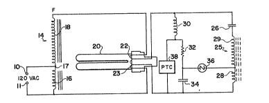
Fig. 1 is a schematic circuit diagram of a first
embodiment o~ a starting and vperating circuit in
accordance with the invention;
Fig. 2 is a schematlc circuit diagram of a second
embodiment of a starting and operating circuit in
accordance with the invention; and
: Flg. 3 is a sche~atic circuit diagram of a third
embodiment of a starting and operating circuit in
accordance with the invention.
Description of the Preferred Embodiments
: Referring ~irst to Fig. 1, the circuit includes
terminals 10 and 11 which are connectible to a 120 volt
AC line voltage souroe, thes~ terminals being connected
to a lag ballast indicated generally at 14. As will be
2~ recognized ~y those skilled in the art, other forms of
ballasts can be used, bu~ the lag ballast is a suitable
form f~r the present circuit.: Balla~t 14 includes a
primary portion 16 and a secQndary portion 18, the
: primary portion extending from the beglnning of the
: 30 windlng which is connect~d to t~rminal 11 to a tap 17which is connected to terminal 10. :The second portion
exte~nds from tap 17 to the ~inish of the winding. A
super compact fluorescent lamp 20 is provided with
r; ~
131 1260
~ilaments 22 and 23 within the lamp envelope. one
terminal of filament 22 is connected to the finish end
o~ the transformer and one terminal of filament 23 is
connected to the start end. The lag ballast i~
arranged so that the voltage from the .start end to the
finish end i6 about ~40 volts AC under open circuit
condltions.
A puI e circuit includes a pulse trans~ormer
indicated generally at 25 and a coupling capacitor 26.
In the embodiment shown, the pulse transormer has a
primary portion 2R and ~ secondary portion 29 with an
intermediate tap. The pulse transformer is in an auto-
transformer form with the secondary winding having
signi~icantly more ~urns than the primary so that a
step-up action result~. The pulse transformer is
connected in series circuit relationship with capacitor
26, this serieB circuit being connected between the
remaining terminals of ~ilaments 22 and 23.
A charging ~ircui~ also connected across these
terminals of the filaments inclu~es a radio frequency
(RF) choke 30, a charging resistor 32 and a storage
: capacitor 34, the~e components being connected in
series relationship with each other. A two-termina}
breakdown device such as a SIDAC 36 is connected at one
end to the ~unction between resistor 32 ~nd capacitor
34 and at the oth~r end to the tap between the primary
: and secondary portions of the pulse transformex.
Finally, a positive temperature coefficient (PTC)
resistor 38 is connected in parallel circuit relation-
ship with resistor 32 and capacitor 34 and in series
with choke 30.
When the circuit is ~irst energized, current
initially flows from the ballast through filament 22,
through the RF choke 30, which presents a very low
~3~ 1260
impedance to the 60 hertz line voltage current, and
through the series~parallel circuits including resistor
32, capacitor 34, and PTC resistor 38. ~owever, PTC
resistor 38 is selected to have a ~old resistance which
is significantly lower than the impedance of the
circuit including resistor 32 and capacitor 34.
Accordingly, substantially all of the initial current
~lows thr~ùgh PTC resistor 38. This current then flows
through filament 23 and back to the source. Capacitor
26 is a relatively small value capacitor (0.01 mfd) and
is chosen to present a hi~h impedance at 60 hertz but a
low impedance at the higher frequency at which starting
pulses will be produced.
Since substantially all of the current is flowing
through the PTC resistor, there is no current to
provide a significant charge on capacitor 34. However,
as this ~Ifilament preheat" curr2nt continues to flow,
not only are the filaments warmed but also the PTC
resistor is heated. As the PTC resistor reaches its
design switching temperature, the resistance thereof
rapidly increases to a high magnitude, signi~icantly
above the impedance of the resistor-capacitor parallel
circuit, causing the current through the PTC resistor
to drop abruptly and causing a voltage c10s2 to tha
op~n circuit voltage of the ballast to appear acros~
the PTC element, forcing the charging of capacitor 34
through resistor 32.
When the voltage across capacitor 34 reaches the
breakdown voltage o~ SIDAC 36, the SIDAC becomes
conduct$ve and places a voltage approximating the
: ballast open circuit voltage across primary 28 of pulsetransformer 25, inducing a high voltage, resulting from
the turns ratio of the transformer, across the
131 1260
secondary of the pulse transformer whic~h is applied to
the lamp, causing lamp lgnition.
Each high voltage starting pulse contains
approximately ~ive milli~oules of energy to provlde
excitation ~nergy ~or ths pulse transformer, circuit
losses, distributed capacitance chargillg, and lamp
ionization. The majority of this energy, placed across
the lamp, induces ionization therein. The time
constant of resistor 32 and capacitor 34 is adjusted to
provide three to four starting pulses on each half
cycle of the 60 hertz supply. Coupling capacitor 26
blocks the 60 hertz current, as mentioned before, but
conducts the high frequency high voltage pulses to the
lamp which now has hot filaments. Choke 30 prevents
the high ~requency from being loaded down by the
circuit including xesistor 32, capacitor 34 and PTC
resistor 38, and the normal ballast impedance of choke
30 prevents the high frequency pulses from being loaded
down by the parallel coils 18 and 16.
When the lamp ionizes and starts its normal
operation, it draws approximately 300 milliamperes and
cIamps the rms voltage across it to approximately 110
volts, thereby causing the starting circuit to be
disabled during normal lamp operation. However, the
PTC element is maintained in its high impedance state
by a trickle current which cuntinues to flow as a
result of the 110 volts across the starting circuit.
If the power should be momentarily interrupted,
the voltage across ballast 14 again increases to 240
volts. Since the filaments are already warm, and since
PTC resistor 38 iB still in its high impedance state,
capacitor 34 immediately begins to charge, reinitiating
a normal restart process. If either one of filaments
22 or 23 burn~ out, i . e ., becomes open , the high
~31 ~260
vol tage starting system is automatically disabled since
it is no longer supplied with power from the ballast
secondary. Thus, the application of high voltage
pulses to the lamp, socket and associated components is
eliminated, contributing to a ~afer and longer life
product. If desired, one or more power factor
capacitors can be added to th~ circuit of Fig. 1. As
mentioned above, the circuit can also be used with a
240 volt reactor ballast or lead type ballast, i~
de~ired.
The circuit of Fig. 2 takes a somewhat dif~erent
approach t~ the problem and employs the ballast itself
as the pulse transformer. Terminal~ 40 and 41 of the
Fig. 2 circuit are connected to line voltage and to the
primary portion 42 of a lag ballast indicated generally
at 43. A power factor correction capacitor 45 is also
shown connected across the primary.
~allast 43 also has a secondary portion 46 with a
: tap 47 near the finish end of the winding. A l~mp 20
has filaments 22 and 23, as in Fig. 1, and one terminal
o~ filament 22 is connected through the ballast 43 to
the source while one terminal of filament 23 is
connected to the common end of the ballast and the
common line of the source. A coupling capacitor 49 is
connected between the terminals of filament 22.
A storage capacitor 50 and an RF choke 52 are
connected in series circuit relationship with each
other between tap 47 and the upper terminal of filament
: 23. A breakdown device, such as a SIDAC 54 i5
connected between the junction vf capacitor 50 with
choke 52 and th~ connection of capacitor 49 to filament
: 22, placing the SIDAC in a serie~ circuit including
capacitor 49, the tapped portion of secondary 43
131 ~260
between tap 47 and the fin~sh end o~ the winding, and
capacitor 50.
It should be noted that the value of capacitor 49
is selected so that it presents a high impedance ~o 60
hertz but a lower impedance to high fre~uency signals.
Choke 52, on the other hand, presents a low impedance
to 60 hertz current and a high impedance to higher
frequencies.
In operation, when the ballast is energized, the
open circuit voltage appears across the ballast coils,
causing storage capacitor 50 to be charged as current
flows from tap 47 through capacitor 50 and the RF choke
and returns to the common side of the line through lamp
filamPnt 23 which presents a low impedance. When the
charge across capacitor 50 reaches the breakdown level
of the S`IDAC, the SIDAC becomes conductive, thereby
causing substantially the entire voltage on capacltor
50 across the tapped portlon of the ballast secondary~
By transformer action, high voltage lamp starting
: 20 pulses are generated across the total secondary winding
of the ballast. Because of the bypass action of
capacitor 49, the high frequency pulse generated is not
caused to flow diractly through filament 22. In the
present circuit, one starting pulse i5 generated each
half cycle, although it would be possible to select
circuit values so that more than one pulse could be
generated each half cycle if required.
The high voltage start~ng magnitude is
intentionally set at a level at which it is not
sufficient to ~tart a cold filament lamp. For a 26
watt lamp, the pulses have a peak value o~ about 1500
volts~ Thus, the lamp does not start immediately but,
rather, filament current is allowed to ~low each half
cycle after the SIDAC has become conductive. This
131 1260
heating current flows from the finish end of the
ballast through filament 22, through the SIDAC, through
choke 52 and through filament 23. Depending upon the
initial conditions of the lamp temperat:ure, after one
or several cycles, the ~ilaments are heated
su~ficiently to permit starting at a lower voltaye
level. Because of the fact that the high voltage lamp
starting pulses are being applied along with the
filament heating current, the lamp starts when
thermionic cathode conditions are reached. Xeeping the
high voltage pulses at a lpw level avoids "forcing" the
lamp into ionization and prevents damage to the lamp
components.
After the lamp has started conduction, the
starting mechanism is automatically disabled because
the ~40 volt open circuit voltage from the ballast i5
no longer available, the lamp clamping the voltage to
approximately 110 volts.
The circuit of Figr 3 is very similar in principle
to the circuit of Fig. 2 but employs a different form
of ballast and, additionally, includes a positive
"turn-off" feature which functlons in the event that
the lamp fails ln any way. As shown in Fig. 3, the
line voltage which, in this case, is 240 volts, is
connected to terminals 60 and 61 and a power factor
correction capacitor 63 is connected between those
terminals. A ballast reactor indicated generally at 65
i5 connected in the "hot" line between terminal 60 and
one terminal o~ a filament 22 in lamp 20. A storage
capacitor 67 is connected in series circuit
relationship with an RF choke 69 between a tap 68 on
ballast 65 and the common side of the power line. A
small bypa~s capacitor 70 is connected in series with
this circuit and between the terminals of filament 23
1 31 1 260
to bypass high frequencv pulse energy. A bypas~
capacitor 72 $s similarly connected between the
terminals of filament ~2. A three-terminal breakdown
device illustrated as a triac 74 has a switchabl
conductive path connected between a terminal o~
filament 22 and the junction between capacitor 67 and
choke 69. The gate of triac 74 is connected through a
two-terminal breakdown device such as a diac 76. Ths
other end of diac 76 i conn~cted to the junction
between a resistor 78 and a capacitor 79 which form~ a
timing circuit to positively control the breakdown of
diac 76 and the firing of triac 74.
In addition, a heating resistor 80 is connected
from the finish end of ballast 65 to thP junction
between capacitor 67 and choke 69, resistor 80 being in
good heat conduoting relationship with a negative
temperature coef~icient resi~tor 82 which i~ connected
in parallel with capacitor 79.
In operation, when power is supplied, capacitor 67
begins to charge through the circuit including choke 69
and capacltor 79 charges through resistor 78 and
capacitor 22. When capacitor 79 reaches the breakdown
level of diac 76, the d~ac becomes conductive,
triggering triac 74 which discharges the capacitor 67
thro~gh the t~pped portion at the finish end o~ reactor
65, the current pul~e causing, by transformer action, a
pulse to be produced across the lamp. Again, the pulse
is insufficient to start a cold lamp but cause~ current
~low through filaments 22 and 23. Depending upon
environmental conditions and the initial temperature of
the lamp, one or several su~h pulses elevatP the
temperature of the filaments to the point at which the
pulses are suficient to initiate ionization. Thus,
the circuit opera~ion ~ substantially similar to that
1 3 1 1 260
of ~ig. ~. However, the incorporation of a triac
(which could also be replaced by back-to-back
controlled rectifiers) allows the separation of
func~ions, higher energy pulse generation, more
accurate positioning of the pulse timing, clrcuit ~eed~
back and also permits the incorporation of a failed
lamp turn-off circuit.
The lamp turn~off circuitl including resis~or 80
and NTC resistor 82, opera e6 by heating resistor 80
after successive applications of high voltage pulses,
causing sufficient current through the resistor to
elevate its temperature. The heat produced by reslstor
80 is conducted to NTC resistor 82, the xesistance of
which lowers sufficiently to prevent capacitor 79 from
developing enough charge to breakdown diac 76. Thus,
the starting circuit is disabled. The time constant of
th~s circuit can be selected so ~hat lt does not come
into play unless the lamp has failed and ~epeated
starting pulses are applied to no avail.
While certain advantageous embodiments have been
chosen to i}lustrate the invention, it will be
understood by those skilled in the art that various
changes and modifications can be made therein without
departlng from the ~cope of the invention as defined in
the appended clalms.