Note: Descriptions are shown in the official language in which they were submitted.
13~2~ -
LASER BONDING l~PPARATUS AND METHOD
Backoround of the Invention
The present invention is directed to using laser
bonding to connect kwo electrical members together. In
particular, the present invention is directed to the inner
; lead bonding of a tape automated bonding tape (TAB) to the
electrical bumps on an integrated circuit die, such as
semi-conductors. Thermal compression bonding, the current
industry standard for inner lead bonding, uses 15,~00 psi
pressures and 400/ C. temperatures which would have a
~;~ damaging efect if leads were bonded to bonding pads or
bumps coated over semi-conductor structures.
One of the features of the present invention is
to provide the most appropriate laser technology for
bonding.
One of the most important problems in laser
bonding is holding the lead in proper contact with the
electrical bump for having an interface which will provide
intimate contact to provide a good bond without voids.
The present invention is directed to various structures
and methods for holding the electrical leads in contact
with the bumps to insure proper contact for bonding.
:~
~....
2 '~ ~
1 Another feature of the present invention is the
use of particular metal combinations for the electrical
members to be bonded together which optimize the adhesion
between the members and produce stronger bonds.
Another feature of the invention is the proYision
of a production apparatus and method for automatical]y
bonding a plurality of integrated circuit dies to a TAB
tape by laser bonding.
Summary
0 The present invention is directed to a method of
bonding the electrical leads o a TAB tape to contacts and
includes placing the leads and contacts in intimate
contact with each other and bonding the leads and contacts
together at the interfaces with a laser such as a pulsed
YAG laser.
Another object of the present invention is
wherein the lead is prebent to provide a resilient set and
is thereafter pressed into a cantilever spring engagement
with the contact.
Still a further object of the present invention
is wherein the lead is brought into ultimate contact with
the contact by directing a stream of gas against the lead
to hold the lead in engagement with the contact.
Preferably, the gas is nitrogen and preferably the stream
f gas is directed coaxially with the laser beam.
Still a further object is the provision of
coatings to the electrical members which have the property
o~ being easily coupled to the laser radiation and which
has a low melting point.
In one embodiment the lead is of copper and is
coated with tin and the contact is gold. The tin coating
is at least three micro-inches thick, and for providing a
longer shelf life the tin coating is at least 12
micro-inches thick. Qther coatings may be indium and
gallium and mixtures of suitable coatings.
--3--
Still a further object of the present invention
is the provision of a method of bonding the flat
electrical leads of a TAB tape to flat electrical bumps on
an integrated circuit die by aligning the bumps and leads
with each other with the tape positioned above the
integrated circuit. The flat leads are held in ultimate
contact with the flat electrical bumps to form a flat
interface and the leads and bumps are bonded together at
the interface with a pulsed YAG laser. The leads may be
0 brought into an intimate contact with the bumps by
directing a stream of gas against the leads, using an
overlay fixture which includes a flat surface engaging a
predeformed lead which is pressed into a spring engagement
with the bump, or uses an overlay fixture which includes a
lip engaging the lead at a position spaced from the lead
end for pressing the lead into a spring engagement with
the bump or any other method that produces (intimate)
contact.
Yet a still further object of the present
invention is the provision of an automatic bonder for
bonding the flat electrical leads of a tape to flat
electrical bumps on a plurality of integrated cir~uit dies
which includes a laser, means for mo~ing the tape
transverse to the laser beam, means for holding a
plurality of integrated circuit dies adjacent and below
the tape, means for moving the die and tape towards each
other, means for aligning the leads on the tape with the
bumps on the die, and means for holding the leads in
contact with the aligned bumps.
Yet a still further object of the present
invention is wherein the plurality of integrated circuit
dies includes a silicon wafer positioned on a resilient
support on which the wafer has been cut to form a
plurality of dies, with or without means for stretching
the support for separating the integrated circuit dies
--4--
1 from each other for ease of handling the individual dies.
The stretching means may include means for holding the
periphery of the resilient support outside of the wafer,
and a ring movable against the suppo@t at a location
between the holding means and the outside of the wafer.
Another object of the present invention is
wherein first and second electrical members are bonded
together by a YAG laser in which the diameter of the laser
beam is su~stantially .002 inches, has an energy output of
approximately 1/4 to 1/2 of a joule in a time of
approximately one millisecond.
Other and further objects, features and
advantages will be apparent from the following description
of presently preferred embodiments of the invention, given
for the purpose of disclosure, and taken in conjunction
with the accompanying drawingsO
B ef DescriPtion of the Drawings
Fig. l is a fragmentary enlarged elevational view
of a TAB tape with an integrated circuit die in place for
bondiny,
Fig~ 2 is a schematic perspective view of one
method of moving a laser beam for bonding a plurality of
bonds,
Fig. 3 is a fragmentary perspective view of a
laser beam bonding the inner leads of a TAB tape to the
bumps on an integrated circuit die,
Fig. 4 is a graph showing the wave form of a
pulsed YAG laser,
Fig. 5 is an elsvational view, partly schematic,
illustrating one structure for bonding a die to a tape,
Figs. 6A and 6B are enlarged sequence fragmentary
elevational views showing one structure for placing a lead
in pressurized contact with a bump,
~ 3 ~
Figs. 7A and 7B are enlarged sequence fragmentary
elevational views showing another structure for plac;ng a
lead in pressuried contact with an electrical bump,
Fig. 8 is an enlarged fragmentary elevational
view illustrating another embodiment of placing an
electrical lead in pressurized contact with an electrical
bump,
Fig. 9 is an elevational detailed view showing a
gas nozzle coaxially with a laser beam for pressurizing a
0 leaa intocontact with a bump,
Fig. 10 is an elevational schematic of an
automated laser bonding system,
Fig. 11 is a fragmentary elevational schematic
view of another automated laser bonding apparatus,
Fig. 12 is a cross-sectional view taken along the
line 12~12 of Fig. 11,
Fig. 13 is a cross-sectional view taken along the
line 13-13 of Fig. 11, and
Fig. 14 is a cross-sectional view taken along the
line 14-14 of Fig. 13-
Description of th~ Preferred Embodiment
While the present invention will be described,for purposes of illustration only, of the laser bonding of
tape automated bonding and TAB lead frames to integrated
circuits, the present method and apparatus for laser
bonding is applicable to bonding other types of electrical
members to each other.
Referring now to the drawings, and particularly
to Fig. 1, the reference numeral 10 generally indicates a
portion of a tape automated bonding tape (TAB) having the
usual sprocket holes 12 and plurality of inner leads 14
; for bonding to an integrated circuit die 16 having active
semi-conductor circuitry.
-6- ~ 27~
1 Current industry standards for TAB inner lead
bonding uses conventional thermocompression bonding with
high pressures and temperatures (currently 15,000 psi and
400 C.) which is acceptable for bonding leads located over
bare silicon. Conventional thermocompression bonding is
not suitable for bonding over semi-conductor structures.
However, it would be advantageous to locate the bonding
bumps over active circuitry to allow reduction in the cost
of the assembled integrated circuits and improve
performance by reducing signal path lengths. Furthermore,
the yield and reliability of bonds over bare silicon can
be increased by greatly reducing heat and pressure.
Thus, the present invention is advantageous by
using laser bonding, where a localized, concentrated
heating source, a laser beam 15, is used to bond the inner
leads 14 to the bumps 18 on an integrated circuit die 16,
as shown in Fig. 3. In a typical lead-bump connection,
the bumps are square bumps 25 microns thick with each side
approximately 4.4 mils long. The leads 14 are 1.3 mils
thick and 3 mils wide.
The first problem considered is which of the
available laser technologies is the most appropriate for
bonding the leads 14 to the bumps 13.
C2 lasers, which have a wavelength of 10.6
microns, were considered. However, such laser energy is
better absorbed by a heat transfer medium such as flu~
than the metal electrical contacts 14 and 18. Also, due
to its longer wavelength, a C02 laser cannot be focused
to a small enough spot for bonding the lead 14 and-bump 18
and were therefore excluded from consideration.
Since the integrated circuit 16 uses aluminum as
a conductor material, and the base material for the leads
14 and bumps 18 are copper and gold, lasers in the
spectrum between .2 and .3 microns wavelength were
considered. This is a desirable situation as energy at
_7_ ~3~ 27~
1 these wavelengths is well coupled to the leads 14 and
bumps 18 while it is reflected by the underlying aluminum
structures. In this spectrum, excimer lasers were
tested. ~owever, it was found that their radiation was so
well coupled that it ablated the molecular bonds rather
than merely vibrating them to cause melting and therefore
these lasers were rejected.
YAG lasers are solid state lasers with an output
that is either continuous wave ~CW), shuttered with an
acoustical-optic or electro-optic device ~Q-switch), or
pulsed. They ha~e a wavelength of 1.064 microns. The
laser output power as a function of time is different for
each of the YAG lasers. And it was concluded that these
differences have a profound effect upon the suitability of
the laser for bonding. A Q-switch laser permits lasing
only when the Q-switch is open and there is a power spike
of several nanoseconds duration at the beginning of each
pulse which is capable of drilling a deep small diameter
hole in the bond site. The CW laser took considerably
more energy to melt the bumps than the Q-switch laser.
The best test results have been obtained using
the pulsed YAG laser. The power versus time curve for a
pulsed lassr is shown in Fig. 4. In a pulsed laser the
flashed lamps are turned on and off for each pulse. As a
result, there is an e~ponential increase in power output
until a maximum level is reached at which point the power
exponentially decreases. With a pulsed laser, the metals
to be bonded are heated to a maximum temperature at which
time the energy input e~ponentially decreases. The pulsed
laser provides a higher power level at the middle of the
pulse than the Q-switch laser. However, the peak power is
orders of magnitude less than the spike at the beginning
of the Q-switch pulse. This power preheats the bond site
and provides the bond site with the most power when it can
use it most ~fficiently. It also provides decreasing
-8- 1 3 ~ 7 6
power which should tend to allow less internal stress
buildup than the instantaneous drop-off of energy that is
characteristic of the Q-switch or CW laser. It was found
that a 50 watt pulse YAG laser made by Carl Haas GmbH Co.
was satisfactory~
The next problem was how to deliver the laser
beam 15 in Fig. 3 to the plurality of bond sites between
each of the leads 14 and the bumps 18 arsund the perimeter
of the integrated circuit die 16. In order to provide a
0 production oriented system, it is more feasible to have a
system with a moving laser beam instead of moving the tape
10 and die 16. In order to prove the feasibility of laser
bonding, the optical arm beam positioning system that is
on an ESI model 44 laser trimmer, was selected. However,
for higher bonding rates such as would be necessary for a
production bonder, a galvanometric laser beam steering
system is desirable. With this system the parts,
including the die 16, as best seen in Fig. 2, remains
stationary while galvanometers 20 and 22 in the X and Y
axis, respectively, rotate mirrors 24 and 26,
respectively, to direct the laser beam to the desired
location.
; Experimental bonding showed the importance of
holding the leads 14 in uniform, intimate contact with the
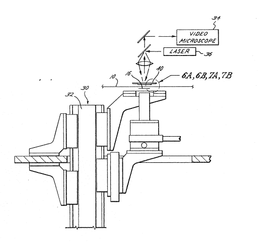
bumps 18. Referring to Fig. 5, a test setup is shown for
determining laser bonding feasibility using a single die
16 for bonding to the tape 10. The test fixture 30 used
an optical rail 32 on which the mount the apparatus
necessary to present the die 16 and tape 10 for
alignment. A video microscope 34 allowed an operator to
view the bond site coa~ially with the path of the laser
36. The fixturing allowed the die 16 to be moved relative
to the tape 10 in four degrees of freedom ~X, Y, Z and
theka (about Z)~ support 38. The tape 10 and die 16 are
-9 11 3~2~
1 shown out of position for ease of illustration of their
relative positions.
While it is a relatively easy task to position
the bumps 18 in alignment with the tape leads 14, it is a
bigger problem to provide a uniform intimate repeatable
interface contact between the leads 14 and the burnps 18.
Usually the TAB tape 10 will not naturally lie
flat due to reasons such as its thin cross section,
interior lead detail, and residual stresses. Therefore,
an overlay fixture generally indicated by the reference
numeral 40 is provided for engaging the top of the tape
10. The overlay 40 aligns the top Q~ the tape 10.
However, merely placing a flat plate against the flat top
of the leads 14 does not always bring the ends of the
leads 14 into a good contact with the bumps 18.
Referring now to Figs. 6A and 6B, an overlay
fixture 40a is seen having an opening 42a for the passage
of the laser beam and is positioned above the lead 14
which is to be mated with a bump 18 on the integrated
circuit die 16. In this embodiment, as best seen in Fig.
6A, the 1ead 14 is preformed or deformed at a poi~t 44 to
have a downward set, for example, 10/ from its original
straight position. The overlay plate or fi~ture 40a is
positioned relative to the lead 14 to engage the point of
deformation 44. As shown in Fig. 6B, the die 16 is then
moved relative to the fi~ture 40a so that the bump 18
makes contact with the end of the lead 14 by traveling
through the distance to which the lead 14 was preformed.
This travel causes a cantilevered spring action of the
lead 14 to provide a uniform contact between the lead 14
and the bump 18. While this lead preforming is a
successful method of achieving satisfactory lead/bump
contact, there are also certain disadvantages. One
possibility is the potential problem that the leads 14 may
be moved in their coordinate positions by preforming.
-10-
Another problem is the requirement of the additional
preforming step.
Referring to Figs. 7A and 7B, another type of
overlay fixkure 40b is shown in which the overlay 40b
includes a ridge or lip 46 on the underside of the fixture
40b which avoids the problem of preforming the lead 14.
As the die 16 and fixture 40b are moved towards each
other, as best seen in Fig. 7A, the ridcle or lip 46
deflects the lead 14 downwardly, such as lOi. As best
seen in Fig. 7B as the die 16 continues moving towards the
fixture 40b the free end of the lead 14 is spring-loaded
against the bump 18 to provide interface contact. The
sturcture of Figs. 7A and 7B eliminates the preprocessing
step of preforming the leads 14.
Referring now to Fig. 8, a third method of
obtaining a contact betwen the leads 14 and bumps 18 is
shown, in this case an overlay fixture 40c. A nozzle 50
is provided to direct gas against the lead 14 thereby
applying pressure against the back of the lead 14 to bring
it into contact with the bump lB. Preferably, as best
seen in Fig. 9, the nozzle 50 is located coaxially with
the laser beam 56. An input gas port 52 is provided
downstream of the last optical lens 54 of the laser system
whereby both gas and the laser beam exit through the
nozzle 50. Experimental results inaicate that the orifice
of the nozzle should be spaced approximately .010 inches
~ to .020 inches above the top of the lead 14. It has also
; been observed that gas pressures in the order of 20 psig
at a flow rate of 4 scfh resulted in a sufficient contact
to provide the necessary pressure for good bonding.
Preferably, the gas is nitrogen as it reduces the
possibility of creating static electricity. Fiber optic
; lights 51 are shown for illuminating the site.
: Another factor to be considered in the bonding of
the leads 14 to the bumps 18 is the types of materials
3 ~
1 used. Experiments with a number of lead finishes and bump
metallurgies have been performed. It has been found that
it is desirable to provide coatings which couple well to
wavelength of the laser used and which have a lower
melting point than the melting point of the leads 14 and
bumps 18. The highest bonding yields have been obtained
when copper leads coated with nominal 25 microinches of
emersion tin were bonded to gold bumps. A cross-sectional
examination of the bonds indicated that there is a
0 void-free, uniform interface between the lead and the
bump. An electron microscope scan taken along the
interface between the lead and the bump indicate regions
of constant composition indicating the presence of alloy
compounds.
The line scans reveal that the principal alloy
that is formed during bonding contains 20% copper and 80%
gold, which is the lowest melting point Cu/Au solid
solutio@. No significant amounts of tin are found in the
bond interface~ However, tin seem to aid energy coupling
(tin is a very good absorber of YAG radiation) and wetting
without forming brittle interim metallic compounds. This
situation appears to be unique to laser bonding.
When the copper in the lead of a bond cross
section is preferentially etched~ the top of the copper
lead, where the laser beam was focused is completely
melted and has alloyed with the other materialsO Below
the melted region there is a region where the copper
plating has been heated enough to recrystallize the
structures that were formed during electro-deposition of
the copper. The third region of the lead is adjacent to
the bond interface. ~o melting of copper has occurred,
and the grain structure of the region is exactly as it was
when the copper was plated. The cross section shows a
metallurigical bond formation that is unique to laser
bonding. Normally, when tin/lead solder is used to join
-12- ~3~ 2~
1 two metals, the solder is the only material that is
melted. The molten tin desolves the materials that are
joined. If gold is one of the materia]s to be joined,
brittle gold/tin intermetallic compounds are formed.
However, in the case of laser bonding tin plated copper
leads to gold bumps, the tin easily absorbs the laser
energy and due to its low vapor pressure, does not boil
away. Rather, it promotes melting on the top of the
copper lead. The molten tin and copper flows over the
sides of the lead then be-tween the lead and the bump. The
tin in the reaction zone produces intermediate phases with
copper and gold which melt below the melting point of the
elemental metals. In this way/ atomic copper and gold are
introduced into a liquid environment sooner in the
pulsed/temperature cycle and full alloying is accelerated
and enhanced. The molten material in the bond interface
also promotes conductive heat transfer so that sufficient
laser energy is coupled to the lead and the bump so that a
sound metallurgical bond is formed. Finally, as
solidification succeeds, the tin is driven out of the
copper/gold solution since the solubility of tin in molten
copper and gold is so low, thus preventing the foxmation
of brittle intermetalic compounds in the body of the bond.
The amount of free tin on the lead also has a
direct bearing on the bondability of the lead. When tin
is plated on the leads, initially all of the tin is pure,
free tin. Over time, the free tin reacts in the solid
state with the copper to form Cu6/Sn3 compound. The
longer the tape sits, the thicker the copper/tin compound
and the thinner the free tin layer becomes. While the
copper/tin compounds have a much higher melting point than
free tin, it is still considerably lower than the melting
point of elemental gold and copper so that it also
contributes to the bonding phenomenon described above.
However, if the free tin layer is too thin, not enough tin
-13- ~3~
is presen~ to absorb the radiation and initiate the
melting/heat transfer process. Experience and limited
experiments show that at least three microinches of ~ree
tin is required to achieve satisfactory laser bonds to
gold bumps. Experience has also shown that if the leads
are plated with at least twelve micro-inches of
electroless tin the tapes can be stored in a dry box for
over two months before a detrimental amount of copper/tin
compound is formed.
The fact that the bonded lead has three distinct
regions of thermal reaction within a height of 1.4 mils
indicates that there is a very steep thermal gradient.
The temperature of semi-conductor structures below the
bond site have been experimentally determined to be in the
neighborhood of 100 C. It has been determined that by
using laser bonding, it is feasible to bond leads to bumps
on semi-conductor structures.
Most of the bor.ding experiments were performed
using tin plated copper leads over gold bumps. However,
experiments with other material combinations have also
been performed. For these experiments, leads were either
bare copper or copper electroplated with tin, silver,
gold, zinc, nickle or indium. All leads were either
bonded to either gold or copper bumps. With the exception
of zinc, all of the lead materials bonded to bumps made
; from other materials. Zinc has high enough vapor pressure
that it boils away before it can flow between the lead and
bump to promote heat transfer. Indium, on the other hand,
like tin, has a low vapor pressure and a low melting
point. Bonds that were made with indium plated leads are
very similar in appearance to those made with tin
plating. Other suitable coatings may include gallium and
mixtures of suitable coatings.
After the laser bonding process developed were
consistent, high yield bonds were made, samples were
-14-
1 bonded and subjectsd to environmental testing. Eight
parts were bonded. Thirty-two leads, the first and last
four on each side, were tested to obtain the pull
strengths prior to environmental testing. Next, two
samples were subjected to one of the following tests:
high temperature storage (500 hours at 150 C. PER
MIL-STD-883C.), 85/85 (500 hours at 85 C. and 85% R.H.),
air-to-air thermal shock (1000 cycles between minus 65 C.
and 150 C PER MIL-STD-883C.~ and liquicl-to-liquid
temperature shock (1000 cyles between minus 55 C. and
125 PER MIL-STD-883C.). The parts were removed from the
environments at regular intervals and pulled tested.
Throughtout the test, all pull tests exceeded 50 grams.
While the prototype system used for feasibility
demonstration, shown in Fig. 5, is capable of making 5 to
6 bonds per second, higher bonding rates are desirable for
use in a production environment and bonding rates in
e~cess of 200 bonds per second are achievable with
equipment such as is shown in Fig. 5. Referring now to
~ 20 Fig. 10 a schematic of a semi-automatic bonder generally
- indicated by the reference numeral 60 is shown in which a
tape 10 is movable horizontally by suitable sprockets 62
across a laser beam 64 from a laser 66. Integrated
circuit dies 16 are positioned under the tape 10 and are
moved into alignment with the tape 10 in the X, Y, Z and
theta directions by a support 66. Image processor 68
measures when alignment is accomplished. A system
controller 70 actuates the laser 66 and a motion interface
72 to control the sprockets 62 and the support 66 for
operating the apparatus 60.
Another more automatic system is shown in Figs.
11 and 1~ generally by the reference numeral 80. In this
case, the tape 10 is supported by rollers 82 from a
support 84 which is movable upwardly and downwardly and
the tape 10 is movable horizontally as well. Preferably,
~;
-15- ~ 3~ ~2~
1 the laser system includes the coaxially air nozzle 50
shown in Eig. 9.
As best seen in Figs. 11, 12 and 13, a silicon
wafer generally indicated by the reference numeral 86 is
supported on a resilient material 88 such as Nitto tape
which in turn is supported from a metal ring 90 and a
stretch ring 92. The silicon wafer 86, while on position
on the resilient material 88, has been conventional cut to
form a plurality of integrated circuit dies 16. The rings
90 and 92 are supported on a support 94 having a control
96 for moving the dies in the X direction, control 98 for
moving the dies 16 in the ~ direction, a control 100 for
moving the dies in a rotational or theta direction and a
control 102 for moving a single die in the Z direction.
While the silicon wafer 86 has been cut into a
plurality of integrated circuit dies 16 as is
conventional, it is desirable to separate the cut dies 16
a small distance apart from each other for ease of
handling. Initially, the wafer 86 is placed upon the
resilient material 88 which has been secured to the metal
ring 90, at which time it is then sawn to form the
individual dies 16. Thereafter, as best seen in Fig. 14,
the stretching ring 92 is mated with the ring 90 to
radially stretch the resilient material 88, radially
outward towards the circular ring 92, which separates the
adjacent edges of each die 16 a small amount 104.
In operation, the apparatus 80 of Figs. 11-14 is
operated by moving the tape 10 horizontally by the rollers
82 and then moving the structure 84 downwardly to bring
the tape 10 down on a die 16. The controls 96, 98 and 100
are operated to align the bumps 18 of a particular die 16
with the leads 14 at a particular location on the tape
10. Gas, such as nitrogen, is injected through the inlet
port 52 and out the nozzle 50 to hold the leads 52 into a
pressurized contact with the bumps 18. The laser beam 56
-16- 1 3 ~
1 is actuated to sequentially bond each of the leads 14 to
each of the bumps 18 on the aligned @ie 16 while the die
is positioned on the resilient material 88. The die
vertical moving support 102 is then raised in which four
pins 106 (Fig. 14) project through the material ~8 for
raising the now bonded die 16. At the same time the tape
10 is raised by the support 84 and moves horizontally
carrying the now bonded die off. The tape 10 is again
moved horizontally and vertically over another unbonded
0 die 16 and the process is r4peated.
The present invention, therefore, is well adapted
to carry out the objects and attain the ends and
advantages mentioned as well as others inherent therein.
While presently preferred embodiments of the invention
have been given for the purpose of disclosure, numerous
changes in the details of construction, arrangement of
parts, and steps of the process, will be readily apparent
to those skilled in the art and which are encompassed
within the spirt of the invention, and the scope of the
appended claims.
What is claimed is: