Note: Descriptions are shown in the official language in which they were submitted.
~ 3~2~
DIGITAL KEY TELEPHONE SYSTEM
The invention is in the field of small telephone
systems and the like, sometimes referred to as key telephone
systems. More particularly, the invention relates to
signalling and supervision messaging functions in a digital
key telephone systern, one example of which is disclosed in a
co-pending application entitled ~Digital Key Telephone
System~, serial number 578,754, which was filed on 28
September 1988 by George Irwin et al.
Background of the Invention
Some examples of small telephone systems have been
generally referred to as key telephone systems.
Traditlonally a key telephone system is provided by extensive
telephone line and control lead wirlng between key telephone
sets. Each key telephone line extends to a telephone
exchange. Each of the telephone sets includes a plurality of
push button switches or keys, each for connecting the
telephone set to a particular telephone line among a
plurality of telephone lines routed to the key telephone set.
The switching function of line selection is mechanically
provided and distributed among the key telephone sets. Any
features in addition to plain ordinary telephone service
(POTS) must be added on a per line basis. The primary
advantage of these systems is economy with small size.
However, if such a system is required to expand along with
the organization it serves, over a time it eventually becomes
more expensive on a per line and feature basis than a private
branch exchange wouId be. Key telephone systems are also
~, .
2 ~ 2 ~3~
characteristically of the analog signal type, and therefore
are impractical to interface with an ISDN as will likely be
desired by business customers in the near future.
Summary of the Invention
It is an object of the invention to provide a
telephone system wherein the functional advantages of key
telephone systems ~nd digital signal communications are co-
existent via station apparatus connected to the system.
In essence, an example of the key telephone system
includes a central unit ~KSU), and a number of stations.
Stations may be, but are not limited to be, telephone sets.
Other forms of stations include data sets and inter~ace units
to C.O. trunks. A general purpose computer, for example a
personal computer, may act as a station, with a suitable
interface u~it. Stations are connected to KSU ports using
digital signals over twisted wire pairs. Some stations may
physically be part of the KSU, and be connected thereto by
means other than twisted pair. The ~SU itself may include
more than one physical unit.
A primary function of the key telephone system is
to provide point to point communication between the stations,
in the form of switched, bidirectional, 64 kb/s channels. In
one example, each station has access to two such channels.
Each station also has access to a 16 kb/s S and S channel
used for system purposes such as si~nalling and supervision.
Each station, and the KSU, contain some form of processing
device, for example, a software controlled microprocessor, vr
~ .
~3~
a logic network. The S and S channel allows one station at a
time to send a digitally encoded message to the KSU. More
specifically, it allows the processing device at the station
to send such a message to the processing device in the KSU.
S This reference to processing devices should be assumed
wharever the action of a station or the KSU is mentioned.
~he S and S channel similarly allows the K~U to send a
message to any one or more stations.
Each message is of a defined format. In this
example there are two formats, each of which require control
information. Depending on the control information in an
incoming message to the KSU, the KSU may retransmit that
message to stations as just described. Hence, a station may
indirectly ~end a message to any other station or to all
stationst by relying on this KSU operation. The KSU operates
in accordance with information contained in the messages, to
set up and tear down 64 kb/s circuit connections between
stations. Stations use such a connection for PCM Yoice ~ or
for data, or as another means to exchange messages.
The operation of a station is controlled directly
by the processing element at that station. The processing
element runs a low level program, and may run higher level
programs. The low level program controls indicators and
other devices at the station, senses the state of input
devlces, and handles generation and interpretation of
messages. A higher level of pro~ram may control the
sequences of operation of the station, and co-operate with
other higher level programs at other stations or in the KSU
~ 3 ~
to provide desired operation of the key telephone system as a
whole. The behaviour of a station is determined by the
program running in that station, or by messages received from
a program running in the KSU. The operation may be wholly or
partially determined by a program running in some other
station, includin~ the case where that station is attached to
or incorporates a gener21 purpose digital computer.
Since the behaviour of a station may be determined
by the program running in another station, it is possible to
add new types of stations, as such become available, or to
install new software in existing stations, to affect the
behaviour of previously connected stations. Thus an added
station may provide new features, possibly requiring novel
sequences of keystrokes and display and indicator operation.
15 Th~ new feature i5 or may be made available at existing
stations without reprogramming those stations or the KSU.
The added station providing the new feature may in
fact be a reprogrammable device such as a personal computer.
Thus new features may be added solely by software change or
addition in an attached computer system, by techniques
generally avallable, without participation of the key
telephone system manufacturer or vendor. Of course, all of
this extreme freedom of access to and control of the
communication functions and features may be subjected to the
typical security and priority etters.
The invention is embodied in a key telephone
system, for providing digital signal communication paths
between a plurality of ports and for providing a signalling
2 ~ ~
and supervisio~ link between, any of 6aid ports and a
processing device in the key telephone system. The key
telephone system includes communication paths being operable
to provide n pairs of time division multiplex transmit (TDMT)
and time division multiplex receive (TDMR) channels, each
channel including a plurality of bit positions. At least one
TDMT, TDMR channel pair is exclusively associaked with each
port. Each said TDMT channel and said TDMR channel includes
a signalling and supervision (S and S~ bit position, in said
plurality of bit positions. A switching means is operab e to
provide communication paths between ones of the TDMT and TDMR
channels, to the exclusion of said S and S bit positions, as
directed by the processing device. An interface means,
responsive to the processing device, transfers information
from the S and S bit position of a selected TDMT channel to
the processing device and transfers information from the
processing device to the S and S bit position of at least one
of the TDMR channels, independently of the communication
paths provided by switching means.
A key telephone system, in accordance with th~
invention, comprises a plurality of ports for connection of
any of a station apparatus and an interface apparatus, each
apparatus including a processing device for controlling its
functions. A synchronous communication medium provides at
lPast one bidirectional communication channel and a message
channel at each port. A synchronous switch means transfers
information between selected ones of the bidirectional
channels in response to control signals. A central processor
~ 3 ~
routinely identifies message channels fro~ which a message
from one of said processing devices is receivable, and in
response to a received message, at least generates one ~f the
control signals and at least one address for d~fining a
message channel for which a message for a corresponding one
of said processing devices is destined. An interface means
identifies a request to send, in response to a first
predetermined signal characteristic in one of the message
channels, previously identified by the central processor, for
soliciting and xeceiving said message. The interface means
also transfers destined messages to message channels as
directed by the central processor.
The invention is also a method of operating a Xey
telephone system having a central processor and a plurality
of station apparatus, each of said station apparatus having a
processiny device for controlling functions of the station
apparatus in response to key control action of a user origin
and in response to messages received via the central
processor. The method comprising the steps of:
a) providing at least one bidirectional time
division multiplex channel in association with each of the
station apparatus;
b~ providing at least one time division multiplex
message channel in association with each of the station
apparatus;
c) routinely selecting one of said station
apparatus for transmission of a message Yia its associated
message channel;
~L3~2~
d) exchanging call set up messages between the
central processor, a calling station apparatus and a called
station apparatus; and
e) in response to a predetermined message, from
t~e called station apparatus synchronously exchanging
information between the bidirectional time division multiplex
channels associated with the calling and called station
apparatus.
The invention is also a method of signalling and
supervi.sion communication in a telephone system having a
central processor and a plurality of ports, each being
available for connection of an apparatus thereto, each such
apparatus including, a processing device for controlling
functions of the apparatus, and an interface device for
exchanging ~ignals in an operating signal format of the port.
The method comprises the steps of:
a) providing at least one time multiplexed message
channel in association with each of the ports;
b) routinely selecting one of said apparatus for
transmission of a signalling and or super~ision message via
its port associated message channel; and
c) exchanging messages, in a predetermined one of
a plurality of message protocols, between the central
processor and said apparatus.
Z5 The invention is also a method of communicating
signalling and supervision messages in stimulus and
functional protocols in a telep~one system having a central
processor and a plurality of ports, each of the ports being
11 3 ~
available for connection of an apparatus, each apparatus
including a processing device for controlling functions of
the apparatus in response to reception of signalling and
supervision messages in one of said stimulus and functional
protocols, and an interface device for exchanging signals in
an operating signal formal of the port. The method comprises
the steps of:
; a) providing at least one time multiplexed message
channel in association with each port;
b) routinely selecting one of said ports for
transmission of a message from its associated apparatus, and
in the central processor receiving a message, from the
selected apparatus, said message being in one of said
stimulus and ~unctional protocols;
c~ in the central processor, generating stimulus
messages and functional messages;
; d) transmitting each of said stimulus messages via
a message channel associated with an apparatus for which the
stimulus message is destined; and
; 20 e) transmitting each of said functional messages
via a plurality of message channels, at least one of which is
associated with an apparatus to which the functional message
is addressed.
~ This invention is also a method of operating a
; 25 telephone ~ystem wherein signalling and supervision messages
of higher and lower levels of protocol are exclusively
compatible with functional terminal apparatus and stimulus
9 ~ 3 ~
terminal apparatus, respectively. The method comprises the
steps of:
a) emulating a functional terminal on behalf of
each stimulus terminal apparatus connected to the telephone
system;
b) exchanging signalling and supervision messages
of the lower level protocol exclusively between step a) and a
calling or a called one of the stimulus terminal apparatus;
and
c) relaying an in-oming signalling and supervision
message of the higher level protocol to each of the terminal
apparatus with an exception being that of performing step a)
on behalf of a stimulus terminal for which said higher level
protocol signalling and supervision message includes
information.
Furthermore, the invention is a method of util~zing
a feature apparatus in a telephone system having a central
processor and a plurality of ports, each of the ports heing
: available for connection of an apparatus thereto, each such
: 20 apparatus including a processing device for controlling
functions of the apparatus, an~ an interface device for
exchanging signals in an operating signal format of the port.
The method comprises the steps of:
a~ providinq a plurality of said apparatus being
connected at a corresponding plurality of said ports, at
least one of said apparatus being a telephone station
apparatus and another of the apparatus being said feature
apparatus;
~L 3 ~
b) providing at least sne time multiplexed message
channel in association with each of the ports;
c) routinely selecting one of said apparatus for
transmission of a signalling and or supervision messaye via
its port associated message channel; and
d) in response to a feature request action of a
user at said telephone station apparatus, exchanging
signalling and supervision messages ~etween said telephone
station apparatus, said feature apparatus and said central
p-ocessor whereby said feature is provided by said feature
apparatus on behalf of said telephone station apparatus.
Yet further~ the invention is a method of
relocating an apparatus being connected at one port to
another port in a telephone system, the telephone system
havin~ a central processor and a plurality of said ports,
each of the ports being available for connection of an
apparatus thereto, each such apparatus including a processing
device for ontrolling functions o~ the apparatus and an
~- interface device for exchanging signals in an operating
signal format of the port. The method comprises the steps
o~:
a) providing at least one time multiplexed message
channel in association with each of the ports;
b) routinely selecting each of said ports for
transmission of a signalling and super~ision message from any
of ~aid apparatus connected thereto;
c) at each port connected apparatus, in response
to a first occurrence of step b), transmittiny a si~nalling
and supervision message including an identifier unique to
said apparatus;
d) in at least one location in the telephone
system and via said mess~ge channel, generating an
maintaining a record, of port location and said unique
identifier in association with each of said port connected
apparatus; and
e) in response to an occurrence of step c) and in
the event that said unique identifier is of record in step
d), recording an instant port location ~t which said
apparatus is reconnected, whereby said apparatus is
automatically relocatable at any port in the telephone system
in response to its physical connection thereto.
Yet further, the invention is a method of replacing
an apparatus with another apparatus at one port of a
~elephone system, the telPphone system having a central
processor and a plurality of said ports, eash of the ports
being available for connection of an apparatus thereto, each
such apparatus including a processing device for controlling
functivns of the apparatus and an interface device for
exchanging signals in an operating signal format of the port.
The method comprises the steps of:
a) providing at least one time multiplexed message
channel in association with each of the ports;
b) routinely selecting sach of said ports for
transmission of a signalling and supervision message from any
of said apparatus connected thereto,
~L3~$~
12
c) at each port connected apparatus, in response
to a first occurrence of step b) transmitting a signalling
and supervision message including an identifier unique to
said connected apparatus and an iden~ifier unique to a
predetermined type of said connected apparatus;
d) in at least one location in the telephone
system, maintaining a record of default features and
characteristics of a plurality of predetermined types of
apparatus connectable at ports of the telephone system;
e) in at least one location in the telephone
system, and via said message channels generating and
maintaining a record of port location, features,
characteristics said unique identifier and said type
identifier in association with each said port connected
15 apparAtus;
f) in response to an occurrence of step c) and in
th~ event that said unique identifier differs from that
associated with any of said ports, performing one of,
i~ downloading said characteristics and
features to the instant port connected apparatus in the event
that said type identifier corresponds to the type identifier
which was mode of record in step e), and in step e) altering
the record of the uni~ue identifier to correspond to the
uni~ue identifier of the instant port connected apparatus,
and
ii) downloading type default features and
~ characteristic, maintained in step d), and corresponding to
: the type identifier of the instant port connected apparatus,
~ 3 ~
13
in the event that the type identifier differs from that which
was made of record in step e), and in step ~) altering the
record of the unique identifier and the type identifier to
corre~pond to those of the instant port connected`apparatus;
S whereby one port connectecl apparatus may be
replaced by another apparatus and be automatically operable
in the telephone system.
Yet even further, the invention is a method of
communicating signalling and supervision messages in stimulus
and functional protocols in a telephone system having a
central processor and a plurality of ports, each of the ports
being available for connection of an apparatus, each
apparatus including a processing device for controlling
functions of the apparatus in response to reception of
signalling and supervision messages in one of said stimulus
and functional protocols, and an interface device for
exchanging signals in an operating signal format of the port.
The method comprises the steps of:
a) providing at least one time multiplexed message
channel in association with each port;
b) routinely selecting one of said ports for
transmission of a message from its associated apparatus, and
in the central processor receiving a message, from the
selected apparatus, said message being in one of said
stimulus and functional protocols;
c3 in the central processor, generating stimulus
messages an~ functional messages;
:~3~$~
14
d) transmitting each of said stimulus messages via
a message channel associated with an apparatus for which the
stimulus message is destined, and
e) transmitting each of said functional messages
from the central processor via each of the message channels.
Brief Description of the Drawinqs
An example embodiment is described with reference
to the accompanying drawing in which:
Figure 1 is a block diagram of a key telephone
system in accordance with the invention;
Figure 2 is a ~lock diagram of a software
architecture for supporting FUNCTIONAL station apparatus in
the key telephone system in figure l;
Figure 3 is a block diagram of a software
:: 15 architecture similar to the software architecture illustrated
in figure 2, but with an added capability of supporting
STIM~JLUS station apparatus as well as the FUNCTIONAL station
apparatus;
: Figure 4 is a graphical illustration of operating
timing pulses and or signals generated within a circuit
: switch module used in figure l;
~igure 5 is a block diagram of a timing ~equence
generator used in the circuit switch module for providing the
timing signals illustrated in figure 4;
Figure 6 is a block schematic diagram of counterst
used in a circuit switch module in figure 1, and arranged to
provide time slot and channel addresses for operation of the
circuit switch module;
~ 2~
Figure 7 is a block schematic diagram of a
converter circuit used in the circuit switch module in figure
1 ;
Figure 8 is a graphical illustration of various
timing signals used in the operation of t:he converter circuit
in figure 7;
Figure 9 is a block schematic diagram of a time
switch circuit used in the circuit switch module in figure 1
to provide circuit switched communication paths in the key
telephone system;
Figure 10 is a block schematic diagram of a time
switch conference circuit in the circuit switch module and
used in combination with the time switch circuit of figure 9
to provide a conference feature in the key telephone system;
Figure 11 is a block ~chematic diagram of an
interface circuit used in the key telephone system
`~ illustrated in figure l; and
Figure 12 is a block schematic diagram of a
processor interface circuit used in th~ key telephone system
: 20 illustrated in figure 1.
Description of the Example Embodiment
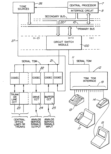
In figure 1 a digital key telephone system provides
for connection of various digital telephone instruments, as
exemplified at 13 and 14, and various digital data terminals,
~: 25 personal computers vr the like, as exemplified at 15 and 17,
:,:
which are able to communicate, Yia the system, with one
another a~ appropriate, and with other devices via line or
~ 3 ~
16
trunk circuits 230 The lines and or trunks serve to connect
the digital key telephone system with other telephone
facilities, for example a central office or priv~te exchange,
not shown. A back bone of the digital ~ey telephone system
is provided by a short parallel time division multiplex (TDM)
bus 10, which provides a wide band communication path between
up to nine 64 channel circuit switch modules 100, a central
processor interface circuit 8 and tone sources 26. If any of
the tone sources 26 provide an analog signal, such is coupled
into th2 system via a lead 27. The bus 10 is referred to as
a primary bus, and a secondary bus 20, similar to the primary
bus 10, provides for unidirectional communications from the
interface circuit 8. Each of the circuit switch modules 100
couples 64 ten bit transmit serial channels to predetermined
corresponding time slots in the bus 10, and up to 64 parallel
selected TDM time slots on either of the buses 10 or 20 to 64
ten bit receive serial channels. 32 of the serial transmit
and receive channels are coupled to an internal ports circuit
12 via a serial TDM path 11. The remaining 32 serial
~0 transmit and receive channels are coupled to external port
circuits at 22 via a serial TDM path 21. Each of the
channels is capable of transmitting a binary signal pulse
stream at a rate of 80 kilo bits per second, with at least 64
kilo bits per second being available as a channel for pulse
code modulated (PCM) voice information, or data information.
The remaining sixteen kilobits may be committed to
supervisory and signalling communications, in association
with the PCM or data information. In this example the
~3~ ~26~
internal ports circuit 12 consists of sixteen TDM time
compression multiplex (TCM) interfaces. The TCM method of
~ignal transmission is sometimes referred to as "Ping Pong"
transmission. Each of these interfaces provides a transmit
path between each of ~CM links 19 and two predetermined and
fixed serial TDM channels in the serial TDM path 11. In a
similar manner analog signals are interfaced to and from
various circuits shown at 23, 24 and 25, via the serial TDM
path 21 and the external ports 22 provided by CODEC circuits.
Alternately, it may be advantageous to provide an external
TDM port for interfacin~ with another telephone facility via
a digital signal trarsmission link, Tl or DS30 for example.
However in this case, each CODEC circuit interfaces with a
predetermined and fixed transmit and receive channel pair of
the ~erial TDM path 21. Hence, for each and every port ~that
is a place where a di~ital telephone instrument or other
digital device or a digitally interfaced or compatible line,
trunk and the like may be connected to the digital key
telephone system), there is at least one predetermined ten
bit parallel time slot in the primary bus 10 which is
allocated to receive information from the line appearance.
In an alternate example, the time slots on the bus 10
correspond to line appearances for the purpose of
transmitting information thereto. However, such alternate
example is not herein further discussed. A central processor
7 i~ coupled via the interface circuit 8 to the primary bus
10 ~or communication via a predetermined 32 of the ten bit
parallel time slots. The interface circuit 8 may receive all
2 ~ ~
18
ten ~i~s of each ~ime slot on the bus 10. Normally, only the
two bits corresponding to a ~ixteen kilobit sub-channel are
transferred from the bus 10 to the central processor 7 by the
interface circuit 8, for purposes of call control. ~he
interface circuit 8 provides signalling and supervision from
the central processor 7 via thP secondary bus 20 at time slot
occurrences corresponding to intended line appearance
destinations via the appropriate circuit switch module 100.
Therefore each circuit switch module 100 transmits 10 bits to
the primary bus 10 but receives and switches only 8 bits from
the primary bus 10. The other two bits are received at the
appropriate time via the secondary bus 20.
In this example, each port associated communication
path provides for full duplex operation with two words, of
;. 15 ten bits each, being exchanged every 125 micro seconds. In
at least one of these words, bit positions 0-7 are dedic2ted
to one of data or voice, the bit:position 8 is dedicated to
signalling and supervision, and the bit position 9 is
dedicated to validation Or signalling and superv~sion. The
signalling and supervision information is collected from, and
distributed to, the port associated channels via the
lnterface circuit 8 under the direction ~f the central
processor 7. The collected information is ga~hered into byte
; groupings by the interface circuit 8 for transfer to the
central processor 7 and by a somewhat complimentary function,
information is distributed from the central processor 7, via
the interface circuit 8 into bit position 8 of a selected one
of the channels or of all the channels.
~ 3 ~
19
The key telephone system is intended to support two
generically different types cf station apparatus: one being
a very basic tele~hone station set hereafter referred to as a
STI~JLUS set or an S set, which includes a bit stream
interface device, a simple processing device, and a CODEC;
and the other being a more complex featured autonomous
station apparatus which may take the fo~n of a proprietary
key telephone set, interface apparatusj or proprietary
display telephone or data terminal. Such instrument :is
referred to as a FUNCTIONAL set and such reference is
intended to indicate that the apparatus contains some call
processing instructions in the form of software or firmware.
For convenience, any station apparatus which is not an S set
is hereafter referred to as a FUNCTIONAL set or an F set.
In the S setl any change in its operating state,
for example ON HOOK to OFF HOOK or a key depression, is
communicated to the central processort via the S set
processing device, the bit position 8 and the interface
device. This is accomplished in the S set by a continuous
(request to send RTS) assertion of "00" in the bit position 8
and 9 of the outgoing channel, until a validated clear to
send ~CTS) is received in bit positions 8 and 9 of the
incoming channel. When the CTS is recognized in the S set a
STIMULUS protocol message indicating OFF HOOK is transmitted
via the S and S bit positions 8. Thereafter, a typical call
progress proceeds by way of exchange of STIMULUS protocol
messages
~3~ ~ 2~
By way of exemplary contrast in the F set, a
request to send (RTS) may be generated after an OFF HOOK is
followed by sufficient telephone call dialing information
having been keyed in by a telephone user. In this case the
processing device and its operational programing perform
basic call processing, and in addition to providing dial tone
at the appropriate moment, may also generate ring back or
busy tone. The F set communicates similar to the S set,
using the S and S bit positions 8. After a CTS is received
from the central processor the F set transmits a FUNCTIONAL
protocol message.
Table 1 illustrates structural arrangements of
messages of STIMVLUS protocol and FUNCTIONAL protocol.
_ __ _ _ Table 1
15 HEADER TYPE LENGTH
:Binary ~HEX)
OXOOOOOO (4OH)
to STIMULUS 1 BYTE
20 OXOlllll r5FH~ __
OX100000 (60H)
to STIMULUS 2 BYTES
OXlOQlll l67H~_ _
25 CX101000(68H)
to STIMULUS MULTI-BYTE
OX101111~5FH~
__
~ OXllOOOO~70H)
; to FUNCTIONAL VARIABLE
OXllllll (7FH)
In the header, bit positions left to right are 7
through 0. In particular, bit positions 5 and 4 indicate the
protocol of the message. FUNCTIONAL messages in this
2 ~ ~
21
arrangement are indicated by both of the bit positions 5 and
4 being asserted "1". S STIMULUS MESSAGES are indicated by
at least one of the bit pos.itions 5 and 4 being asser~ed "O".
The purpose of each of the bit positions in the header is
illustrated in Table 2.
. _ Table 2
BIT 7 65 4 _ 3 2 1 0
PURPOSE START CLEAR PROTOCOL SECONDARY
TO INFORMATION
_ SEND _ _
In the case of a header being in a range of 4OH -
5FH, the header is the actual message, the gist of which is
carried in the bit positions 3-0. In messages of more than
one byte, the second and subsequent bytes carry information.
The quantity or number of the information bytes within a
messa~e are specified in lesser significant bit positions of
the header.
The CTS bit position indicates a clear to send
message and is only of significance when received by an ~ set
or an S set.
Plural protocols and central processor flow control
of messages, communicated via the S and S bit positions,
:permit advantageous software architectures as illustrated in
figures 2 and 3, to be resident in a key telephone system as
: 25 shown ln figure 1 In fiyure 2, a key system unit (RSU) 40
includes common equipment 41 coupled with an S and S channel
50 via software elements, namely a network controller 42 and
a data base m~nager 43. The common equipment 41 is in effect
';
. ' ;
' ' ' ' , ' ' :
. '
~L 3 ~
22
representative of a hardware interface with the buses 10 and
20 in figure 1 but also includes firmware and software
resident in the central processor 7. In this example, the
central processor 7 is provided by a 68008 microprocessor
available from Motorola Corp., of 1303 East Algonquin Road,
Roselle, Illinois, 60196, U.S.A. The central processor 7 is
arranged to support modularized software elements such as the
elements 42 and 43.
The S and S channel is a message channel which is
in operational effect common to all the FUNCTION station
apparatus of the sy~tem. Exemplified are F sets 51 and 52,
an automatic call distribution (ACD) terminal 53, a system
management data retrieval (SMDR) terminal 54 and an outboard
trunk unit 55 for connection to a central office ~not shown).
Each of these is a FUNCTIONAL apparatus which includes its
own processing device and call processing software.
Figure 3 illustrates an example of an architecture
configured similar to figure 2, but for supporting STIMULUS
sets in addition to FUNCTIONAL sets. In this case, the
common equipment 41 also supports additional modular software
in the form of FUNCTIONAL emulators 45, 46 and 47. These
FUNCTIONAL emulators perform, on behalf of respective
STIMULUS sets 61 and 62, and a STIMULUS trunk unit 63, to
make these appear to the rest o the key telephone system to
also be FUNCTIONAL sets. Hence, in some system
configurations, economy on a per port basis is achieved. It
should be noted that FUNCTIONAL elements 52-54 may also be
~ 3~ 2~
23
present in figure 3 but were omitted for convenience of
illustration.
In operatiQn of the key telephone systems in
accordance with figure 2 or 3, any F set receiving a CTS
message is able to transmit to all FUNCTIONAL entities, be
these apparatus or emulators. Likewise, F emulators are able
to transmit to all FUNCTIONAL entities but as the F emulators
are software based in the KSU, the previously discussed
arbitration ritual of RTS and CTS is not required. Any
10 FUNCTIONAL entity which may thus respond or act in accordance
with its own programing as warranted by the content of the
transmitted FUNCTIONAL message. Any such FUNCTION~L message
involving a STIMULUS set is intercepted and subsequently
acted upon by the corresponding FUNCTIONAL emulator software
module. This effectively results in a series of STIMULUS
messages being exchanged between the FUNCTIONAL emulator and
its associated STIMULUS set via its S and S channel. For
example, S set 61 and emulator 45 exchange mes'sages via an S
and S channel 6~a.
2 0 In FUNCTIONAL messaging the message bits are
distributed or relayed to every channel occurrence in each
frame. Although STIMULUS sets or units are thus exposed to
the FUNCTIONAL messages, the STIMULUS processor devices
therein are arranged to disregard FUNCTIONAL messages as
recognized by the distinct header as illustrated in the
foregoing tables 1 and 2. ~n the other hand, STIMULUS
messages are unidirectional. Distribution of a STIMULUS
message is confined to the channel ooourrence which
,
.
1 3~2~
2q
corresponds to a STIMULUS set for which the STIMULVS message
is destined.
Flow control of FUNCTIONAL and STIMULUS messages is
discussed fro~ a hardware viewpoint after the following
discussion of the structure and operation of the modular
circuit switch module 100 with reference to figures 4-10.
In order that each of one or more circuit switch
modules 100 be able to transfer information from the serial
rDM paths 11 and 21 to the parallel TDM bus 10 without
contention, a phased timing sequencer, as shown in figure 5,
resides within each of the modules 100 for regulating the
functions of the module. Wave forms exemplified in figure 4
illustrate a master frame timing pulse occurring at a rate of
1 Khz, clock pulses numbered 0-27 occurring at a rate of 5.12
MHz and state machine timing pulses SMO-SM10. With the
switch module 100 installed in the system, a preset start
decoder 101 is connected to a hard wired location, not shown,
which provides an identity, that is a fixed four bit binary
word, ID0-ID3. The combination of the signal states of the
bits ID0-ID3 is unique for each possible switch module
location in the digital key telephone system. The preset
start decoder 101 generates a 5 bit binary word on a bus 102,
in response to the combination of bit states as shown in
table 1. A five bit counter 103 is preset by each occurr~nce
of the master frame pulse, to correspond to the word on the
bus 102 and thereafter is incremented with each occurrence of
a clock pulse. An output 104 of the counter 103 is decoded
by a decoder 105 which generates a reset signal on a lead 106
~ 3~
with each occurrence of a count of 19 in the counter 103.
Thus with the occurrence of the next clock pulse, the counter
103 is reset to a count of zero. Thus a modulo 20 counting
function is provided, which is phased as is illustrated in
table 1.
TABIE 3
_
Cn~l~T ID3 ID2 lDl ID0 ~ET T~M-ll ToM-21
;SWITCH V~LUE OF ~ AND ~E AND
10 MODULE BUS 102 TIME s~r ~E s.~oT
O~ ~ENCE O~RRESP~NDENOE
.
o 0 0 0 0 18 0 2
1 0 0 0 1 17 1 3
2 0 0 1 0 14 4 6
3 0 0 1 1 13 5 7
: 4 0 1 ~ 0 10 ~ 10
0 1 0 1 9 9 11
6 0 1 1 0 6 12 14
7 0 1 1 1 5 13 15
8 1 0 0 0 2 16 1~
_ _ . _ _ _ . . _ .
.
In accordance w th the table, for example for the
circuit switch module 0, the channel zero on the serial TDM
path 11 is inserted onto the parallel TDM bus 10 in time slot
zero, channel one in time ~lot 20 and so on until the last
channel, chann 1 31, of a serial TDM fra~e is inserted into
time slot 620.
... . . . . .
.
~3~ $~
26
Stated in other te~ns, each TDM path has 32
parallel ten bit receiving channels assigned to it on the
primary bus 10, and each of these channels is separated from
the other by 19 other channel occurrences.
The decoder 105 also generates an SM0 timing pulse,
coincident with the count of 19 occurring in the counter 103.
A shift register 109 responds to the SM0 timing pulse and the
clock pulses to generate additional timing pulses SM1-SM10 as
illustrated in figure 4.
Referring to figure 6, the time slot occurrences on
the parallel TDM bus 10 are tracked by a parallel slot
counter which includes a modulo 20 counter 111 and a modulo
32 counter 112. The counter 111 responds to the 5.12 MHz
clock pulses to provide repetitive counts of 0 through 19 on
five time slot count leads TSC 0-4. The counter 112 is
incremented with each reset occurrence in the counter 111 to
provide repetitive counts of 0 through 31 on five time block
count leads TBC 0-4, whereby in combination binary signals on
the TSC and TBC leads define 640 parallel time slot addresses
per frame. A serial channel counter function is provided by
a counter 113 which provides 32 channel counter addresses on
serial channel count leads SCC 0-4 to define channel
occurrences in the serial TDM paths 11 and 21. The counter
113 is incremented with each time block occurrence as
indicated by the timing pulse SM6. All of the counters 111,
112 and 113 are reset with each occurrence of the master
frame pulse.
L K ~
27
The converter circuit illustrated in figure 7
resides within the circuit switch module 100 and performs
both serial to parallel conversions and parallel to serial
conversions for each of the 64 TDMT and the 64 TDMR channels
on the ~DM paths 11 and 21. As before mentioned, the TDMT
channels are incoming and carry data or voice, plus
signalling bits originating at the terminal instruments,
while the corresponding TDMR channels are outgoing, each to
the originating terminal instrument. Each incoming time slot
includes 10 binary bits which are converted directly to
parallel form and asserted during the predetermined time slot
interval on the primary bus 10. Each outgoing time slot
incl~des 10 binary bits which are obtained from one of two
sources: one source being a corresponding time slot interval
on the secondary bus 20; the other source being 8 bits from
`:
any time slot interval on the primary bus 10, the 8 bits
having traversed the time switch, plus 2 bits from the time
slot interval on the secondary bus 20 corresponding to the
TDMR channel occurrence.
The converter circuit is di cussed in more detail
with reference to the timing signals illustrated in figure 8.
A SYSTEM CLOCK waveform shown at the top of figure 8, and
some of the other waveforms in figure 8 are idealistically
depicted for convenlence as having vertical rise and fall
portions. Actually, in practice these waveforms have sloped
rise and fall portions similar to those waveforms illustrated
in figure 4, whlch are more realistically depicted. The
converter circuit, in figure 7, includes three orthogonal
, .. .
28
shift registers shown at 501, 502 and 5U3 respectively.
These three registers perform the required serial to
paral]el, and parallel to serial conversions~ Each of the
orthoganal shift registers 501, 502 and 503 is associated
with a clock generator, not shown, which produces non-
overlapping timing signals, illustrated in figure 8, for
shifting and directional control. Vertical directional
control signals Vl, V2 and V3 are used to vertically direct
shift functions of the register 502, 501 and 503
respectively. ~orizontal directional control signals Hl, H2
and H3 are ~Ised to horizontally direct shift functions of the
registers 502, 501 and 503. The actual loading of D type
flip flop elements in the registers 502, 501 and 503 is
clocked by signal pulses Sl, S2 and S3. The control signals
V2 and V3 are shown in broken line to indicate that these
signal pulses are 20 system clock periods removed from the
adjacent H2 and H3 signal pulses, such that each co~mences at
40 system clock intervals.Bits of the TDMR serial bit streams
are timed to be coincident with the rising edges of a serial
digital loop clock signal C690. Bits of the TDMT serial bit
streams on the paths 11 and 21 are sampled and re-timed to
likewise be co-incident, by latches 511 and 521. A half
cycle of the system clock prior to the rising edge of the
serial digital loop clock signal C690, contents of the (2 ~y
8) outgoing register 502 are selected by a receive
multiplexor 535 to provide the first bits of each of the TDMR
channels at 11 and 21. The receive multiplexor selection is
in response to a MUX SEL OUTGOING control signal shown in
~ 3 ~
29
figure 6. The outgoing bits are timed by the rising edge of
the clock signal C690 to start transmission of a 10 bit time
slot. Shortly thereafter, the starting bits of the
corresponding TDMT channels are sampled by the latches 511
and 521 using the falling edge of the same clock signal C690.
The sampled bits are then applied to the (2 by 2) incoming
register 501. During the said same clock siynal C690,
contents of the register 502 and the incoming register 501
are asserted in parallel by a multiplexor 532 on the leads of
the primary bus 10. Only in an instance of a time slot (TS)
19 occurrence, which is indicated by a rising edge of a
decode 18, in Figure 6, will the multiplexor 532 gate Z bus
signal states to the P bus 10. A half cycle of the same
system clock signal after the falling edge of the said same
15 C690 clock signal, the three orthogonal registers 501, 502
and 503 are clocked, resulting in the incoming register 501
accepting said starting bits, the outgoing register 503
moving the second outgoing bit to the multiplexor 535, and
the register 502 moving 8 bits of the TDMT path 21 toward the
20 multiplexor 532. At the same time the incoming register 501
moves the remaining two bits toward the multiplexor 532 via a
multiplexor 53 The next two outgoing parallel information
bytes are moved through data holding registers 504 and 505,
under control of timing signals SM2 and SM6 and hence, into
the register 502. At the same moment, as before described,
the register 501 stores the first two bits of each incoming
TDMT channel. Once the first two bits have occurred, the
registers 501 and 503 receive no further clock signals until
, , ~
', ' ~ ' , ' ~ ` '
,
. ' , .
$ ~
the start of the next outgoing time slot sequence when all 10
registered bits are shifted in parallel toward the P bus 10.
At the start of the ne~t time slot sequence,
registers ~01 and 503 are caused to m~ve their respective
S contents (2 bits) vertically, that is upwardly in figure 5.
Thereafter the next eight TDMT bits are shif~ed vertically
into the register 502 and the previous contents are liXewise
shi*ted out to be transmitted via the multiplex~r 535 and the
TDMR paths 11 and 21. The horizontal directional control
signals and the vertical directional control signals continue
to be alternately asserted thereby repeating the parallel to
the serial and serial to parallel cycle for each TDM channel
on TDN paths 11 and 21.
The time switch circuit in figure 9 provides for a
timely transfer of 8 information bits from one of the 640
time slsts on the primary bus 10 to a parallel T bus input ~f
the parallel input multiplexor 506 of the converter circuit
in figure 7, and thereby ultimately to a TDM pa~-h (11 or 21)
time slot, as directed by the central processor 7. The
information bits of each time slot on the P bus 10 are
momentarily captured by a data input latch circuit 710 and
thereafter applied at an input 702 of a dual port random
access memory (RAM) 701. The dual port RAM 701 includes an
output 703 which drives a T bus 770 in response to a six bit
address applied at a read access address port 704. The RAM
701 differs from a typical dual port memory device in that
for the purpose of storing information received at its input
702, it does not include the typical address decode
~ 3 ~
31
circuitry. Instead, each write address is d~coded and
applied to an individual one of 64 write enable leads at 706.
The decoded write address is timed via a write enable latch
and strobe circuit 720. Any number of the write enable leads
may be asserted by the circuit 720 simultaneously. The dual
port RAM 701 responds, to a signal asserlion or signal
assertions on any or all of its 64 write enable leads at 706,
by storing the signal states of said 8 information bits at
the corresponding memory location or locations as the case
may be. For example, if none of the leads at 706 is
asserted, no storage locations are written. If one or more
of the leads at 706 is assertecl, the one or more
corresponding storage locations are written. Reading of the
64 dual port RAM storage location occurs sequentially on a
regular and periodic basis, under the control of a flip flop,
not shown, in the latch 711 which is toggled by signals SM2
and SM6, and the 32 sequentially generated TDM channel
addresses which are generated by the counter 113 in figure 6.
A connection memory 730 contains information as to
20 the actual time slots of the 640 P bus 10 time slots from
whence information bit states are stored in the dual port RAM
701. The connection memory 730 is provided by a content
addressable memory which includes an eleven bit data input
port 731, a six bit address port 732 and a 10 bit compare
address port 733. The general structure and operation of
content addressable memories is known. In this example P bus
addresses, from whence information is to be stored, are
lodged in memory locations in the connection memory 730.
1 3 ~
32
Each of 64 memory locations, not shown, correspond with a
separate one of 64 output leads at 7360 A digital
comparitor, not shown, is associated with each of the 64
memory locations such that addresses appearing at the compare
port 733 are each compared with thP information stored at
each of the 64 memory locations. In every instant where thè
address at the compare port 733 and the information at a
memory location is the same and the memory location also
includes an asserted validity bit, the corresponding one of
the 64 output leads at 736 is asserted. The asserted state
is eventually transferred via the circuit 720 to the dual
port RAM 701, which responds as previously described.
Operation of the circuit switch modules 100 is
dire~ted by the central processor 7, which uses the interface
circuit R and 32 dedicated time slots on the P bus 10 for
lodging information into the memory locations of the
connection memory 730 via a data latch circuit 740 and an
address latch circuit 750. The information is delivered from
the interface circuit 8 in the form of four bytes each of
which occupies time slot 1~ of 4 sequentially occurring time
blocks on the P bus 10. The four bytes include a command
byte, followed by an address byte, a low order data byte, and
a higher order data byte. Each of these bytes is asserted
along with a validity signal on one of the two remaining
leads of the P bus 10 which indicates that the bytes are in
fact an instruction from the central processor 7. A portion
of the command byte specifies either a write or a read
function intended for one of a connection memory, a source
~ 3 ~ 3
33
connection memory or a destination connection me~ory. A
comparitor responds to the validity signal and a match
between a remaining portion of the command byte and the ID0-3
by causing the address latch to store the next byte, that is
the address byte. Thereafter the data latch 740, in figure
9, captures 11 bit states of the low and higher order bytes,
which are subsequently stored in the memory location of the
connection memory 730 as indicated by six address bits
asserted by the address latch 750. Provision is also made
for the central processor 7 to confirm the information
content of any address in the connection memory. In this
case the command byte indicates the read function, and the
address byte indicates the memory location to be read. The
subsequent low and higher order bytes are driven by the
stored information from a data output 738 of the connection
memory 730 and via an output latch ?12 and buffer 713 to the
Z bus and thence via the multiplexor 532 in figure 7 onto the
P bus 10 where it is picked up by the interface circuit ~.
The time switch conference circuit in figure 10
provides a three party conference feature in the digital key
telephone system. The time switch conference circuit adds an
ability for a timely transfer of 8 information bits from
another of the 640 time slots on the P bus 10, ultimately to,
for example, said TDM path time slot previously referred to
at the beginning of the discussion of figure 9. Very briefly
by way of introduction, bytes are presented to a multiplexor
992, in figure 10, via the T buses 770 output from figure 9
and via a conference C bus 991. The four most significant
~ 3
34
bit (not including the sign bits) ~f each byte are compared
in a comparitor 993 which directs the multiplexor 992 to
assert the 8 bits from the C bus 991 on the T bus 540 in the
event that the value of the 4 bits from the C bus 991 is
equal or greater than a value of the 4 bits from the T bus
995. In the event the I' bus 995 valuP is greater, then the
bits from the T bus 995 are asserted on the T bus 540 by the
multiplexor 992. Thus a three party conference call may be
implemented wherein each party hears only the instant loudest
speaking party of the other two parties.
Considering the time switch conference circuit o~
figure 10 in more detail, the information bits of each time
sl~t on the P bus 10 are momentarily captured by a PCM input
latch 910 and thereafter applied at an input 902 of a dual
. 15 port RAM 901. The dual port RAM 901 includes an ~utput 903
which is buffered to the C bus 991 via a PCM output latch
circuit 990. Likewise the T bus 770 is buffered to the T bus
995 via a latch circuit 994. The dual port RAM 901 differs
from the dual poxt RAM 701 in that it has only 16 memory
locations and lacks typical address decode circuitry for the
purpose of reading out information stored at these memory
locations. Each write address is dec~ded and applied to an
individual one of 16 write enable leads at 906 and likewise
each read address is decoded and applied at an individual one
25 of 16 read enable leads at 907. The decoded write address is
timed via a write enable latch and strobe circuit 920.
Likewise the decoded read address is timed via a read enable
latch and strobe circuit 970. The read enable latch and
~ 3 3~
strobe circuit 970 also includes an EXCLUSIVE OR logic
circuit not shown, which responds to a single decoded read
address occurrence by asserting a compare enable signal on a
lead 971. The compare enable signal is used to activate the
selection function of the comparitor circuit 993, which in
the absence of the compare enable signal causes the
multiplexor 992 to assert the T bus 995 bit states onto the T
bus ~40, exclusively. Hence if no decoded read address or
more than one decoded read address is asserted at inputs of
;0 the read enable latch and strobe circuit 970, the conference
function does not occur. The dual port RAM 901 responds, to
a signal assertion on a write enable lead at 906, by storing
the signal states of said 8 information bits at the
corr~sponding memory location. Likewise, reading of a memory
1~ location in the dual port RAM 901 occurs in response to a
corresponding read enable lead at 907 being asserted.
source connection memory 930 contains information
as to the actual P bus time slots from whenc~ information bit
states are stored in the dual port RAM 901. The source
2~ connection me~ory 930 is provided by a content addressable
memory having 16 memory locations, not shown, each
corresponding to a separate one of 16 output leads at 936.
The source connection memory 930 includes an eleven bit data
port 931, a six bit address port 932 and a ten bit compare
2~ address port 933. A digital comparitor, not shown, is
associated with each of the 16 memory locations such that
addresses appearing at the compare port 933 are each compared
with the information stored at each of the 16 memory
36
locations. In an instant where the address at the compare
port 933 and the information at a memory location are the
same and the memory location also includes an asserted
validity bit the corresponding one of the 16 output leads at
936 .is asserted. The asserted state represents a decoded
write address, which is subsequently transferred via the
circuit 920 to the dual port RAM 901 which respon~s as
previously described.
A destination connection memory 980 contains
information as to the actual TDMR time slots Gn the TDM paths
11 and 21 to which information bit states stored in the dual
port RAM 901 may be directed via the multiplexor 992 and the
T bus 540. The destination connection memory 980 is of a
structure similar to that of the previously described source
connection memory 930. Addresses appearing at a compare port
983 are each compared with information stored at each of 16
memory locations. In an instant where the information at the
compare port 983 and the information at a memory location are
the same and the memory location also includes an asserted
20 validity bit, a corresponding one of 15 output leads at 986
is asserted. The EXCLUSIVE OR logic circuit in the read
enable latch and strobe circuit 970 permits the corresponding
read enable lead at 907 to be asserted, which causes the dual
port RAM 901 to read out the 8 information bit states from
the corresponding memory location as previously described.
The information appearing at the compare port 983
is asserted from the channel counter bus leads SSC 0-4 by a
channel counter latch circuit 911. The latch circuit 911
~: .
37 13~
al60 includes a flip flop, not shown, which is toggled by the
timing signals SM2 and SM6 and thereby provides 64 addresses
per frame, similar to that previously discussed in relation
to the latch circuit 711.
Operation of the conference function in the digital
key telephone system is directed by the central processor 7,
which uses the interface circuit 8 to communicate with the 32
dedicated time slots on the P bus 10 for lodging information
into the memory locations of the source connection memory 930
and the destination connection memory 980 via a data latch
circuit 940 and an address latch 950 in a manner similar to
that previously discussed in relation to the connection
memory 730. Likewise the central processor 7 may confirm the
information content of the source connection memory 930 by
15 way of a data output 938, a data output latch circuit 912, a
buffer circuit 913 and the Z bus, connected as shown in
~ figure 8. Information content of the destination connection
: memory is also available to the central processor 7 by way of
: a data output 988, a data output latch circuit 914, a buffer
20 circuit 915, and the Z bus, connected as shown in figure 10.
A primary function of the interface circuit 7, as
illustrated in figures 11 and 12, is that of receiving S and
S messages and distributing S and S messages. The S and S
messages are received from the primary bus 10 in one port
related time slot at any one time by S and S receive buffer
registers 810. The S and S messages ar~ transmitted to all
of the secondary bus 20 time slots or to a selected one of
the secondary bus 20 time slots by S and S transmit buffer
38
registers 820. The S and S messages are physically coupled
with the primary and secondary buses lO and 20 by a bus
buffer circuit 801. The interface circuit is similarly
coupled to central processor address and data buses, at 898
and 899, by a processor buffer 805. A primary function of
the buffers 801 and 805 is that of relaying signals between
all of various potential signal sources and destinations
while minimizing the actual number of receiving gates and
driving gates physically attached to the buses and various
unillustrated timing and control leads. Provision of such
buffers is usual in digital electronic systems and does not
warrant detailed discussion.
Another primary function of the interface circuit
is that of capturing requests to send (RTS) an S and S
message. As before described, an RTS occurrence is marked by
'zero' occurrences in bit positions 8 and 9 in a time slot.
A valid signal detector receives each bit g time slot state
and detects and latches the 'one' state for a short time. A
request to send detector 816 likewise receives each bit 8
time slot state. If the valid signal detector 815 is
unlatched and the bit 8 state is 'zero', the RTS detector 816
asserts a request to send signal indication on an RTS lead
816a. If the request to send is from within a selected group
of tlme slots, a receive shift clock (RSCL) causes a shift
register portion of the buffer registers 810 to shift the RTS
indication into the buffer register 818. After sixteen RSC1
pulses, a receive load clock (RLCLj causes the contents of an
intermediate two byte shift register to be transferred to a
1 3 ~
39
two byte output register. The contents of the output byte
register are available at the processor buffer 805 via an S
and S message bus 812. Thus the registers 818 are clocked to
monitor a group of 16 specified ports in the key telephone
system for RTS occurrences. An occurrence of an RTS during
any input from any of the 16 specified ports is arranged to
generate a low level interrupt to alert the central processor
to the presence of information. However, as it is intended
that each port connected apparatus will continuously RTS
until a clear to send ~CTS) is received by it, there is no
particular urgency attached to any one RTS occurrence.
Eventually, the central processor will specify transmittal of
an appropriate CTS and simultaneously select the port related
time slot as a source of an expected S and S message.
When a CTS message is detected in the intended
station apparatus a response, in the form of at laast a one
byte message, is transmitted. The first bit of the message
is a 'one' in the bit 8 position and a valid 'one' in the bit
9 position. This combination causes a start bit detector 817
to raise a start bit (SB) signal for the duration of
subsequent uninterrupted valid signal detection occurrences,
coincident with the selected time slot. In the presence of
the SB signal, RSCL pulses (one per frame) cause bit 8 states
of the selected time slots to be shifted into the S and S
receive buffer registers 810. Interrupt signals are
generated with every byte so collected, such that the central
processor is able to receive and if necessary, internally
encue the incoming~ S and S message.
~3~ 2~
Outgoing S and S messages are received from the
processor buffer 805 ~ia a bus 822 as timed by transmit load
(TL) pulses. A shift register in the register 820 shifts
received bytes, bit by bit toward the bus buffer 801 at a
rate of one bit per frame in response to transmit shift clock
(TSCL) pulses. The state of the output stage of the shift
register is continuously applied to a transmission gate 823.
The transmission gate 823, and an idle bit driver are both
responsive to a time slot select (TSS) signal for this
operation. In the case of an F message, the TSS is asserted
throughout the length of the message continuously, frame
after frame. In the case of an S message, the TSS is
asserted for the duration of the time slot associated with
the destination port of the S message. The idle bit driver
asserts a 'one' on the lead 829 when the TSS is not asserted.
A valid signal driver 825 responds to the TSS assertion by
asserting a 'one' on a lead 826, whereby S and S bit
assertion on the lead 829 are accompanied by valid signal bit
assextion on the lead 826.
Another capability of the interface circuit 8 is
that of providing wide band data paths between any of the
port associated 64 Kbs channels and the central processor 7.
Input is received ~rom any specified channel via a data
receive buffer 830 under the control of a read bus (RB)
strobe, which is generated coincident with occurrence of a
primary bus ti~e slot from which receiving is required. This
occurrence preferably raises a high level interrupt which is
intended to result in a write to processor (WP) strobe being
~ 3 ~
41
generated to provide the buffered byte on a bus 831 for use
by the central prooessor 7. In like manner, bytes of
information are transferred from the central processor 7, via
a data transmit buffer 840 to a bus 841, for assertion during
a predetermined time slot on the primary bus 10.
Although the buffers 830 and 840 provide a
convenient data transport interface, this typ~ of interface
can be unduly time consuming if such transfer are to occur
frequently. For example, frequent data transfers are
required between the switch modules 100 and the central
processor 7, in order to exercise prompt control of
communication paths in the key telephone system. Hence, a
more specialized interface is provided which operates
throughout the 32 time slots on the primary bus 10, which are
dedicated to exclusive use by the central processor 7, as
previously described. Connection instruction bytes are
loaded from a bus 863 to a four byte FIFO 861 via a
multiplexor 860 in the presence of a write (~) signal. After
the FIFO 861 has received four bytes, the central processor
7 must direct the interface circuit to initiate transfer of
data to the circuit switch 100 via a bus 866 and the primary
bus 10. The interface circuit asserts the bits states
appearing at the FI~O output onto the primary bus 10 with
each occurrence of a dedicated control time slot. If no
information transfer is required, an idle code is asserted on
the bus 863 and therefore is subsequently asserted on the bus
866. By this means, up to 32 bytes of connection instruction
can be transferred via the primary bus during each frame. Up
~ 3 ~
42
to 16 bytes of query and 16 bytes of response information may
be ~xchanged via the primary bus 10 by loading the FIFO with
a 2 byte query message.
~unctional circuit blocks in figure 12 interface
- ~ with the central processor 7 via the same processor buffer
805, shown in figure 11. In figure 12, a time slot address
generator 880 similar to that discussed .in relation to figure
5 provides definition of time siot interval occurrences on
the primary and secondary buses for the interface circuit 8.
Particularly, address registers 881 are selectively loaded
via the buffer 805 from the central processor 7 to define;
those time slots which are watched for RTS, that time slot
which is granted S and S message transmission to S ancl S
receive buffer registers 810; and the time slot selected for
single channel transmission of an S and S STIMULUS message or
a CTS message.
In operation, a comparator apparatus 882 monitors
the contents of the address registers 881 and the time slot
address occurrences from the generator 880. Occurrences of
; 20 matches, in combination with instruction of central processor
origin and signals from the detectors 815-817, are used to
generate the controlling signals in sequence and with timing
as previously discussed in relation to figure 11. A status
and interrupt circuit 883, monitors the progress of S and S
message transfer, data byte transfers, and control byte
transfersl with reference to signals of detector and control
origin, to generate timely interrupt signals whereby the
central processor is informed of information exchange
~ 3 ~ s~
43
opportunities and requirements.
:~ :
::
~: :