Note: Descriptions are shown in the official language in which they were submitted.
`'` ~ ` ~3113~ ~
10577-144/T10
STATE MACHINE CHECKER
BACKGROUND OF THE INVENTION
The present invention relates generally to
data processing systems> and more particularly to a
method, and apparatus for implementing that method~ of
monitoring the proper operation of a state machine of
the type operable to sequence through a number of pre-
determined states, producing control signals for con-
trolling various operations of other portions of the
data processing system.
In many of today's data processing systems
there is a need to permit certain portions or subsys-
tems of the system to operate autonomously. One tech-
ni~ue for fulfilling this need is to provide the sub-
system with programmable control in the form of, for
example, a microprocessor and associated support struc-
ture (e.g., memory). Often, it is necessary for twosuch subsystems to communicate with one another such
as, for example, when transmitting data from one to the
other. S~ch communication, often called "handshaking,"
will direct operation of one or the other of the sub-
systems, depending upon the handshake signals. j
An example may be found in the input/output(I/O) system of the data processing system, in whicl~
intelligent subsystems are often used to control data
transfers between various units of the I/O system. For
exa~ple, a typical I/O system will have one or more pe-
ripheral devices controlled by a device controller that
responds to instructions from a central processor unit
(CPU) of the data processing system to initiate and
control data transfers between the CPU and a selected
one of the peripheral de~ices. Data is usually trans-
ferred in a bit parallel, byte (or word) series fashion
between the per.ipheral device and the device controller
~ ~ 1 3l~3a~ ~
during such a transfer. The transfers are controlled
by handshaking between the device controller and the
peripheral device associated therewith. Such handshak-
ing can be generated by microprocessor systems.
However, when speed is a consideration, a
microprocessor system may not be capable of meeting the
demand. An alternative is available: Special state
machines can be designed to perform the handshake-gen-
erating operations necessary, at the required speeds.
For the purposes of the description of the
present invention, it will be understood that a state
machine, which can be implemented in one of any of a
number of presently known configurations, is of the
type that is operable to each of a number of two prede-
termined digital states. The assumption of each digi-
tal state is dictated by the immediately prior digital
state and the state of any event signal that may be
also applied to direct operation of the state machine.
An example of the use of state machines in a digital
processin~ system for issuing memory commands can be
found in U.S. Patent No. 4,672,609.
SUMMARY OF THE INVENTION
The present invention provides a method, and
discloses apparatus for implementing that method, of
checking for proper operation of a state machine to
ensure that it assumes the proper states, in the proper
order, and issues the proper signals. The state ma-
chine being checked by the invention is of the type
that generates control signals, receiving in return
response signals (the control and response signals form-
ing the handshake activity referred to above), in per-
forming various operations. For purposes of the descrip-
tion of the invention, the state machine being checked
will be referred to as the "master" or "checked" state
machine. The state machine that operates in response
~ ~ ~ 3~3~ ~
to the control signals produced by the master state
machine will be referred to the `'slave" state machine.
Broadly, the method of the present invention
comprises the steps of emulating the slave state ma-
chine to sequence through a variety of states in re-
sponse to the control signals generated by the master
state machine; checking each assumed emulated state to
determine if the emulated state is correct; and genera-
ting an error signal in the event of incorrect opera-
tion. In addition, each state assumed by the masterstate machine is checked to ensure its correctness.
Associated with each master state machine is
a checker state machine constructed to emulate the slave
state machine with which the master state machine com-
municates. The checker state machine receives the con-
trol signals generated by the monitored master state
machine, and responds by sequencing through the same
states as the slave state machine with which the master
state machine communicates. Signaling representing the
states assumed by the master and checker state machines
are coupled to a compare circuit where a determination
is made as to whether the then-assumed states of both
the master state machine and the emulated slave state
machine are correct. If not, an error signal is gener-
ated.
A number of advantages are achieved by the -~
present invention. First, the method, and the appara-
tus implementing that method, provide a check to ensure
proper operation of a state machine and its associated
circuitry.
Further, since the emulator state machine can
be configured to be identical to that with which the
master state machine communicates, and both manufactured
in modular form, one can use the module either as a
master state machine (by using the master control signals
generated by the master state machine), or as a slave
state machine (in which case the slave signals would be
~3~ 3~
4 64157-263
used). And, regardless of how used, the checking of the master
state machine can still be made.
According to a broad aspect of the invention there is
provided a method of monitoring proper operation of a state
machine means operable to assume one of a number of digital
states, each assumed digital state being indicative of an
immediately prior assumed digital state and receipt of an input
signal produced by a digital means, the state machine means
generatlng control signals for controlling, at least in part,
operation of the digital means, the method comprising the steps
ofs
emulating the digital means by receiving the control signals
to produce therefrom an emulated input slgnal representative of
the input signal;
comparing emulated input signals and the control signals in a
manner that determines whether the control signals are correct;
and
producing an error slgnal in the event the comparing step
determines the control signals are not correct.
According to another broad aspect of the invention there
is provided in a data processing system having processing means, a
peripheral device and device controller means operable to control
data transfers between the peripheral device and the processing
means, the device controller means and the peripheral device each
having state machine means for generating handshake signals in
response to the handshake signals of the other, apparatus for
monitoring proper operation of the device controller means state
~3~3~
4a 64157-263
machine means, the apparatus comprising:
emulator state machine means coupled to receive the device
controller means handshake signals for emulating the peripheral
device state machine means to generate emulated peripheral device
handshake signals; and
compare means coupled to receive the device controller means
e~l~L~ re~
and~peripheral device handshake signals for determining that the
present device controller means handshake signals are correct, the
compare means including means for generating an error signal when
it is found from said comparison that the devlce controller means
handshake signals are not correct.
According to another broad aspect of the invention there
ls provlded ln a data processing system, includlng a first data
station and a second data station coupled to one another for data
communication therebetween, the first and second data stations
each having control means operable to generate control signals and
to receive response signals from the other of the control means,
each of the control means comprisings
first state machine means operably coupled to receive the
response signals from the other of the control means for
sequentially assuming each of a number of dlgital states and
produce therefrom the control signals;
emulator state machine means coupled to the logic means to
receive the control signals produced by the first state machine
means for emulating the other state machine means of the other
data station to produce emulated response signals that are
substantially the same as the response signals of the other
B
~3~ tc~7~3
4b 64157-263
cont:rol means; and
means for comparlng the emulated response signals and the
control signals for producing an error signal in the event of
dete~cted erroneous operation.
According to another broad aspect of the invention there
is provided in a digital system, including a first and a second
state machine means each operable to sequence through first and
second numbers of digital states, respectively, the first state
machine means being configured to produce control signals in
response to receipt, at least in part, of response signals
produced by the second state machine means, apparatus for checking
proper operation of the first state machine, the apparatus
comprlslng.
third state machine means coupled to receive the control
signals and operable to sequence through a plurality of digital
states to emulate the second state machine means and to produce
emulated response signals that are substantially identical to the
response signals produced by the second control signals; and
means for comparing the control and the emulated response
2~ signals for producing therefrom an error signal when improper
operation of the first state machine means is detected.
These and other advantages of the present inventlon will
become apparent to those skilled in this art upon a readlng of the
following detailed description, which should be taken in
conjunction with the accompanying drawings.
B
;3
4c 64157-263
BRIEF DESCRIPTION OF THE DRAWINGS
Figure 1 illustrates use of master-slave state machines
in a device controller and an associated peripheral device,
forming part of a data processing system;
Figure 2 is a representative timing diagram
illustrating control signals and responsive device signals
produced by the state machines contained in the device controller
and peripheral device, respectively, of Figure 1.
Figure 3 is a block diagram of the control unit
containing the master state machine being checked as used in the
device controller of Figure 1, and showing an associated emulation
of the slave state machine to monitor proper operation of the
master state machine;
Flgure 4 ls a block dlagram of the construction of the
state machlne used either as a master state machlne or a slave
(checker) state machlne; and
Flgure 5 ls a dlagram of the state sequence checker used
ln Figure 3 to check the states assumed by the master state
machlne and the emulated slave state machine.
DETAILED DESCRIPTION OF THE INVENTION
As indicated above, the present lnventlon is used in
conjunction with one, or another, or both, state machlnes
configured as a state machine "couple" to communlcate wlth one
another for cooperatively performlng various operatlons. An
example of one such operatlon
might be the cooperative control of the transfer of
data between a peripheral device and a central process-
ing unit (CPU) of a data processing system. It is this
type of cooperative control performed by the interaction
between two state machines (one the master, producing
control signals that are responded to by the slave state
machine) that forms the environment for the present
invention.
Turning now to Fig. 1, a part of an input/
output (I/O) section of a data processing system is
illustrated. The I/O section, designated generally
with the reference numeral 10, includes an I/O bus con-
structed to connect a CPU (not shown) to a peripheral
device 12 via a device controller 14. In operation,
the device controller 14 is configured to receive in-
structions communicated on the I/O bus from the CPU
(not shown) requesting, for example, status information
o~ the peripheral device 12, or a data transfer either
to or from the peripheral device. The device control-
ler 14, in turn, will communicate with the peripheraldevice 12 by issuing control signals, to which the pe-
ripheral device 12 responds with the device signals.
This CONTROL SIGNAL - DEVICE SIGNAL interchange (typi-
cally referred to as "handshaking") will continue until
the operation initiated by the device controller 14 is
completed - be it a data transfer, or merely a checX of ~
the status of the peripheral device 12. Not shown, for
reasons of clarity, is the bus structure that connects
the device controller 14 to the peripheral device 12
for conducting data therebetween.
The signaling between the device controller
14 and peripheral device 12 may be initiated by either
unit, depending upon the particular operation to be
performed. The signals are generated by control units
20, 22, contained in the device controller 14 and pe-
ripheral device 12, respectively. The contro]. unit 20
operates to generate three CONTROL SIGNALS, illustrated
in Fig. 2 as SELECT OUT, MASTER OUT and SYNC OUT and
the (slave) control unit 22 responds to the CONTROL
SIGNALS with the DEVICE SIGNALS that comprise, as also
illustrated in Fig. 2, in phantom, SLAVE IN and SYNC IN
signals.
A typical colloquy between the state machines
20, 22 may be to control the transfer of data from the
peripheral device 12 to the I/O BUS th~rough the device
B controller 14. The peripheral device~ is first selec-
ted by assertion (i.e., brought HIG~) of the SELECT OUTsignal in Fig. 2. The peripheral device 12, or more
accurately the slave control unit 22 contained in the
peripheral device 12, signifies recognition of the se-
lection by asserting the SLAVE IN signal.
An instruction is placed on the data bus (not
shown) connecting the device controller 14 to the pe-
ripheral device 12, and SYNC OUT signal asserted. The
slave control unit 22 responds by asserting momentarily
the SYNC IN signal, signaling receipt of the instruc-
tion. If the instruction was one requesting data from
the peripheral device, the instruction would thereafter
be followed by assertion of the MASTER OUT signal.
Thereafter, data is placed on the bus (not shown) con-
necting the device controller 14 and the peripheral
device 12 and the SYNC IN signal asserted by the slave
control unit 22 to signify that the data is then present ~
and stable. The master control unit 20 responds by
momentarily asserting the SYNC OUT signal in response
to each assertion of SYNC IN, signaling that the data
has been accepted.
The SYNC IN, SYNC OUT handshakes continue for
each piece of data transferred. When all the data has
been transferred, the slave control unit 22 signals
this by dropping (deasserting) the SL~VE IN signal.
The master control unit 20 responds by dropping the
MASTER OUT signal, which the slave control unit acknowl-
edges by asserting the SLAVE IN signal. In turn, the
1311~
7 64157-263
master control unit 20 responds by dropping SEEECT OUT, and the
slave control unit responds by dropping SLAVE IN.
The particular protocol used to transfer data between
the device controller 14 and the peripheral device 12 is not
important. Any protocol can be used. What Figure 2 is meant to
illustrate, however, is that the respective control units 20 and
22 contained in the device controller 14 and peripheral device 12
function as a couple, cooperatlvely responding to the signaling
produced by the other.
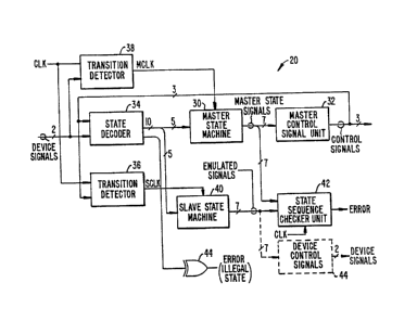
Turning now to Figure 3, the control unit 20 used in the
device controller 14 ~Fig. 1) to generate the CONTROL SIGNALS is
illustrated. As Figure 3 shows, the control unit 20 includes a
master state machine 30 operable to generate master state slgnals
that are communicated to a master control signal logic circuit 32
that produces, from the master state signals, the CONTROL SIGNALS
that are communicated to the peripheral device 12. The CONTROL
SIGNALS are coupled back and applied to a state decoder 34, which
also receives the DEVICE SIGNALS produced hy the peripheral device
12. The CONTROL SIGNALS are al~o applied to a transition detector
36, and the DEVICE SIGNALS are also applied to a transition
detector 38, both transition detectors 36, 38 receiving a system
clock (CLK) signal.
As indicated above, the DEVICE SIGNALS that are received
by the state decoder 34 are produced by a slave state machine,
(not shown), and associated circuitry, contained in the device
controlled by the device controller 14. A substantially identical
(slave) state machine 40 is constructed to be associated with the
B
13113~
8 64157-263
tmaster) state machlne 30, ln effect operating to emulate the
slave state machine (not shown) that forms the heart of the slave
con1:rol unlt 22 of the peripheral device 12. The emulating slave
~ta1:s machine 40 receives signaling from the state decoder 34 that
cau~es it to assume those same states that are assumed by the
state machine of the slave control unit 22. The output of the
slave state machine 40 is applied to a state sequence checker unit
42, as is the output of the master state machine 30. The state
sequence checker 42 checks the outputs in a manner that determines
whether or not each individual state assumed by the two state
machines 30 and 40 are correct; if not, the state sequence checker
42 issues an ERROR signal indicating a problem.
Before commencing a dlscu~sion of the operation of the
circuit illustrated ln Figure 3, lt will be beneficial to the
reader to know and under~tand the architecture of the state
machlnes used in connection with the present invention. Thus,
referring to Figure 4, there is illustrated the architecture of
the master state machine 30. The architecture of the (slave)
state machine 40 is substantially identical, so that a discussion
of the Figure 4 diagram will be understood as applying to either
of the state machines 30, 40.
As Figure 4 illustrates, the state machine 30 includes
an eight-stage state register 50 that receives, at each of the
data inputs of the individual stages (50a, ..., 50h), output
signals formed by a combinatorial logic unit 52. The outputs IS~
S2, ..., S6~ from only seven of the stages (50a, ..., 50g) of the
state register 50 are used to form the state signals that are
B
~3~3~^~
9 64157- 63
applied to the master control signal unit 32 ~Figure 3) and the
state sequence checker unit 42. The outputs S~, ..., S7 of all
eight stages 50a, ..., 50h are coupled back and applied inputs to
the combinatorial logic unit 52, as are the five output signals
produced by the 5-to-N state decoder 34. The combinatorial logic
unit 52 operates to form signal ing on the output lines 54
therefrom indicative of the next state to be assumed by the master
state machine 30. It is clocked into the state register 50 by the
system MCLK slgnal (the slave state machine receives SCLK)
produced by the transition detector 38 (Figure 3).
There are eight states assumable by the master state
machine 30 (or the slave state machine 40). Each state is
represented by a ONE or HIHG in one and only one of the stages
50a, ..., 50h, with the other stages containing a ZERO or LOW.
Thus, at any one moment of operation time, only one of the state
signal~ appearing at the outputs SO, ..., S6 will have a ONE. The
eighth state, a WAIT state, is represented by a ONE in the stage
50h of the state register 50.
In operation, the master state machine will cycle
through various of its eight legally assumable states, depending
upon the operation to be performed, and as it a~sumes each
individual state the output lines S~, ..., S6 are applied to the
master con~rol signal unit 32, a comblnatorial logic formation,
producing the CONTROL SIGNALS that are communicated to the
peripheral devlce 12 (Fig. 1). Depending upon the particular
state the master state machine 30 assumes, and the sequence of
states it has traversed through to assume that state, the control
~3
1 3 ~
64157-263
unit 22 of the peripheral device 12 will also sequence through
various states to produce the DEVICE SIGNALS that are communicated
back to the device controller 14, and applied to the state decoder
unit 34. State changes of the DEVICE SIGNALS are detected by the
transition detector 38 of conventional design, producing an MCLK
pulse each transition from one state to another. The MCLK pulse
is, as indicated in Figure 4, applied to the state register 50.
Operation of the slave state machine 40, as hereinbefore
indicated, is essentially the same except that it changes state
with each change in the CONTROL SIGNALS (detected by the
transition detector 36 that produce the SCLK signal to effect
state changes - if any).
Thus, the next state to be assumed by the master state
machlne 30 ls developed by the state decoder 34, as descrlbed
above. The master ~tate machine is placed in this next state,
however, only when the peripheral device 12 responds to the most
recent CONTROL SIGNAL produced by the master state machine 30.
Thus, when the peripheral device 12 does respond, indicated by a
state change in the DEVICE SIGNALS, the change will be detected by
the transition detector 32, creating an MCLK pulse that will load
the state register 50 with the newly-developed state. This
cooperative action and response activity continues as long as is
necessary to comple~e whatever operation was started.
As indicated above, the slave state machine 40, in
effect "emulates" the state machine (not shown) contained in the
control unit 22 of the peripheral device 12. Thu~, for each state
change made by the master state machine 3~ there may be an
B
lOa 64157-263
ans~ering state change in the state machine (not shown) operating
the peripheral device 12, and the slave state machine 40 also
changes. The output from the state register 50 contained in the
slave state machine 40 will be identical to that of the state
machine forming the control unit 22 in the peripheral device ~2.
As noted above, any one state of the master or slave
state machines 30, 40 is rçpresented by a single ONE being
asserted on one of the output lines S~, ..., S6. Checking becomes
a simple matter of determining whether the master or the slave
state machines have assumed an illegal state (i.e., something
other than a single ONE). This is the principle upon which the
state sequence checker unit 42 is structured: A parity check is
made on the outputs of the state machlnes 30, 40.
This ls illustrated in Figure 5, which shows the
structure of the state sequence checker 42. The master and
emulated state slgnals produced by the master and emulating slave
state machines are respectively applied to parity check circuits
42. ~ach of the parity check circuits are structured to check for
odd
parity; any noted parity error is communicated by an OR
gate to the J input of a J/K flip-flop 68 that is clocked
by the system clock CLK. The K input of the J/K flip-flop
68 is tied to ground G, configuring the J/K flip-flop
as a latch.
As the master and emulated slave flip-flops
30, 40 assume each state, that state is checked by the
parity checkers 62, 64. Thus, insofar as the master
state machine 30 is concerned, not only is the legality
of each state assumed checked, but the circuitry asso-
ciated with the master state machine is checked through
the medium of the emulated slave state machines 40, and
the check performed on that state machine.
A further advantage of the present invention
is obtained if the circuit illustrated in Eig. 3 is
developed in modular form. Included in the circuit
would be a device control signal unit 44 ~shown in phan-
tom in Fig. 3) which develop~ the DEVICE SIGNALS from
the state signals produced by the slave state machine
40. So constructed, the control unit 20 would be used
in either the device controller, in which case the CON-
TROL SIGNALS would be connected as illustrated, or it
could be placed in the peripheral device, in which case
the DEVICE SIGNALS would be connected and communicated
25 to the device controller 14. ; -
The state decoder unit, in light of the fact
that there are five separate signals applied thereto
(three, forming the CONTROL SIGNALS, and two forming
the DEVICE SIGNALS), is capable of producing therefrom
32 separate state identifications. Only ten, however,
are actually used. Thus, the remaining signals are
applied to an EXCLUSIVE-OR circuit configuration 44 to
produce an ILLEGAL STATE signal, thereby checking the
state decoder unit 34.