Note: Descriptions are shown in the official language in which they were submitted.
1311~
1 72434-79
PERIPHERAL CONTROLLER AND ADAPTER INTERFACE
Bac~qround of the Invention
In many data processing systems, a common bus is used to
link together a plurality of units to the system. The bus permits
any two units linked to the system to communicate or transfer ln-
formation between each other.
Typically, communication is established by any unit by
maklng a request to the bus for a bus cycle. When that bus cycle
is granted, th0 requesting unit becomes the master and may address
any other unit, linked to the bus, as a slave.
Transfers requiring a response from a slave unit, such
as a read memory transfer from the slave, require a response
cycle. In these cases, the master indicates a response is requir-
ed and ldentifies itself to the slave. When the required informa-
tlon becomes avallable, the slave will assume the role of the
ma~ter and initiate a transfer of information to the requesting
unit. Thus, with such an interchange, two bus cycles are requir-
ed. During the time it takes the slave to respond, other units
may use the bus to communicate with any other unit that does not
involve the master-slave units above. In the event that two units
request simultaneous service from the bus, tie-breaking logic may
be included at each unit directly coupled to the bus.
~3~C~
To insure that the proper unit is addressed by
a master unit, a channel number exists for every end
point in the system with the exception of the memory
type processing elements. In those cases, a channel
05 number is assiqned to each device along with the
memory address identifying the end point. Some
devices, such as a full duplex device, utilize two
channel numbers. Others, such as an output only or
an input only device, use only one channel each.
Units with multiple inputs and outputs ports
generally require a block of consecutive channel
numbers to distinguish between the different ports.
With such a system, different priorities are
established for accessing the bus. For example,
when a peripheral has access to the bus via a
controller, all other peripherals connected to this
controller would be locked out or denied access to
the bus.
Further details regarding the above type of bus
system is disclosed in the following U.S. patents.
The referenced patents pertain to the proprietary
bus system of Honeywell.
(a) Data Processing System Providing Split-Bus
Cycle operation by Pra~k V. Cassarino, Jr. et
al, issued December 14, 1976, and having U.S.
Patent No. 3,997,896.
(b) Data Processing System Providing Locked
Operation of Shared Resources by George J.
72434-79
Barlow et al, issued December 28, 1976, and having
United States Patent No. 4,000,485.
(c) Data Processing System Having Distributed Priority
Network by George J. Barlow, issued June 14, 1977,
and having United States Patent No. 4,030,075.
(d) Data Processing System Having Distributed Priority
Network with Logic for Deactivating Information Trans-
fer Requests by Geor~e J. Barlow, issued June 20,
1978, and having United States Patent No. 4,096,569.
(e) Apparatus for Processing Data Transfer Requests in a
Data Processing System by Frank V. Cassarino, Jr.
et al, issued November 23, 1976, and having United
States Patent No. 3,993,981.
(f) Data Processing System Having a Data Integrity
Technique by George J. Barlow, issued November 30,
1976, and having United States Patent No. 3,995,258.
Disclosure of the Invention
In accoxdance with the present invention there is
provided a peripheral device control unit for use in a data pro-
cessing system of the type which includes a main processor unit,
a main memory unit and a plurality of peripheral devices, said
system being of the type wherein said processor unit and main
memory unit are coupled to a system bus which provides a path for
communication among said processor unit, main memory unit and
other units which may be coupled to said bus; said peripheral
device control unit being coupled between said bus and said peri-
B
t~ ~
7~434-79
pheral devices to enable communication over said bus between each
of said peripheral devices and other units coupled to said bus;
said peripheral device control unit comprising: a controller,
said controller being coupled to said system bus and comprising a
processor, a sequencer, and a direct memory access(DMA) element;
a plurality of adapters, each adapter being coupled between a
respective one of said peripheral devices and said controller,
each adapter comprising a data buffer, each adapter receiving data
units from the respective de~ice and accumulating said received
data units in the data buffer thereof for subsequent transfer to
said system bus, each adapter accumulating data units received
from said system bus in the data buffer thereof for subsequent
transfer to the respective device, each adapter generating a
request signal (DPPCLX) when the data buffer thereof is available
for a data transfer operation with said system bus; said sequencer
cyclically polling each adapter to enable said adapter to communi-
cate with said system bus during the interval when said adapter
is being polled; said DMA element being coupled to receive said
request signal of each of said adapters during the respective
polling interval and for responding to said request signal to
generate an acknowledgement signal (DMACKX); each adapter being
couplea to receive and respon.d to said acknowledgement signal to
control the transfer o~ qata units between said system bus and the
data buffer thereof during the respective polling interval.
The present in.vention relates to a computer system
having a system bus, a main memory connected to the system bus and
-- 4 --
B
~ 72434-79
a plurality of peripheral devices connected to the bus. The
sys.tem further includes a controller coupled to the bus for
- 4a -
~'~
3 ~ ~
transferring data between each of the plurality of
peripheral devices and main memory in direct memory
access operations. An adapter having a buffer
memory is coupled between each peripheral device and
oS the controller. The controller includes a sequencer
for responding to a demand signal from each of the
plural adapters to generate an individual DMA
request for a direct memory access transfer of a
limited amount of data between main memory and the
adapter making the demand. Each adapter generates
the demand signal (DPPCLX) only when the buffer
memory of the adapter is prepared to servlce a DMA
transfer of the limited amount of data.
Each adapter is further able to receive control
signals, at times other than when a DMA request is
made, for non-DMA transfers of data between the
controller and the adapter. Further, the adapter
responds to the control signals to condition the
adapter for a DMA transfer.
During start-up, after reset of the adapter,
the adapter provides an identification code for
identifying the peripheral device connected to it
when an initial setup control signal is received.
Brief Description of the Drawinqs
The foregoing and other objects, features, and
advantages of the invention will be apparent from
the following more particular description of the
preferred embodiments of the invention, as
illustrated in the accompanying drawings in which
~ 31 ~
like reference characters refer to the same parts
throughout the different views. The drawings are
not necessarily to scale, emphasis instead being
placed upon illustrating the principles of the
05 invention.
Figure 1 is a schematic drawing of a computer
system utilizing a bus architecture.
Fiqure 2 is a block diagram of a computer
system embodying the present invention.
Figure 3 is a more detailed block diagram of
elements of Figure 2.
Figure 4 is an illustration of the connection
between the controller o~ Figure 3 and an adapter to
show the signals between the controller and an
adapter in one example implementation.
Figure 5 is an electrical schematic diagram of
a typical adapter to be connected to the controller
of Figure 3.
Figure 6 is a timing diagram illustrating the
transfer of status data from the adapter to the
controller.
Figure 7 is a timing diagram of the transfer of
command data from the controller to an adapter.
Figure 8A is a timing diagram of a transfer of
information from the adapter to main memory in a DMA
operation.
Figure 8B is a flowchart illustrating the
transfer of Figure 8A.
3 ~ ~
7 72434-79
Figure 9a is a timing diagram of a transfer of data from
main memory to an adapter in a DMA operation.
Figure 9B is a flowchart of the data transfer of Figure
9A.
Detailed DescriPtion of the Invention
A typical data processing system utilizing a common bus
is shown in Figure 1. As shown, a bus 100 which often comprises
multiple lines, is coupled to a memory storage unit 102. The
memory storage unit may comprise ~everal memory storage units,
each in communication with the bus. Also connected to this data
processing system i5 a scientific-arithmetic unit 108 and three
controllerss a baslc device controller 110, a communications
controller 112, and a mass store-magnetic tape controller 114.
The basic controller 110 1~ coupled to the bus to allow multlple
unlt record perlpheral devices 116 to have access to the bus 100.
Uslng the basic controller ln thls manner avolds larger demands on
the bus that would result if each unit record peripheral device
had a direct access to the bus. Slmllarly, a communicatlons
controller 112, which is used to provlde communicatlon control vla
modem devices, and a mass store/magnetic tape controller 114,
which is used to control mass storage devices such as a tape
peripheral device 118 or a disk peripheral device 120, is in
communication with the bus 100.
In addition to the above devlceæ, a central processor
106 is connected to the bus for controlling the bus cycles and
regulatlng data transferred over the bus. Thus, any one of these
devices which are coupled to the bus 100 may address or
communicate with any other unit connected to the bus 100. For
h
13113~
7a 72434-79
example, the tape peripheral 118 may address the memory storage
unit 102 by way of the controller 114.
In accordance with the present invention, a universal
peripheral controller ~UPC) 209 is provided. The UPC may control
different types of peripheral devices without requiring different
controlling devices. As shown in Figure 2, the UPC 209 is coupled
to a system bus 204 by a data bus 207a and an address bus 207b.
the UPC may be coupled along the system bus 204 so that it
receives a higher priority status than other devices coupled to
the system bus 20~. The data bus 207a may be either 16 or 32 bits
wide, and the address bus 207b 24 or 32 bits wide. With such an
interface assembly, communication may be made to and from any
peripheral coupled to the system bus through the UPC.
The UPC 209 may lnterface with up to four perlpheral
adapter~ 212, A-D, where each adapter has one or more channels. A
total of up to eight logical channels are accessible through each
UPC. Typical peripherals which may be coupled to the adapters
212, a~ shown, include a tape peripheral 213, a disk peripheral
214, and a unit record peripheral 215. To insure proper data rate
~. .
13113~ ~
synchronization and error detection, each adapter
provides a buffer for data storaqe.
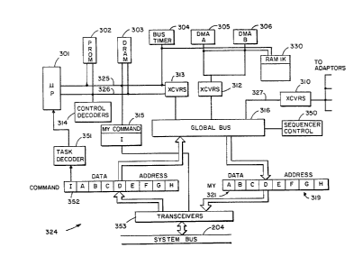
A more detailed block diagram of the Universal
Peripheral Controller 209 is shown in Figure 3. A
05 commercially available~Motorola 68000 type micro-
processor 301 is coupled to an internal data bus 325
and an address bus 326. Coupled to the data bus 325
is a commercially available read only memory (PROM)
302, a commercially available dynamic random access
memory (DRAM) 303, and a MY COMMAND register 315.
The DRAM 303 may have storage capacity for at least
64K words and is provided with random loqic
implementation to refresh information stored
therein. The PROM 302, the DRAM 303, as well as
commercially available control decoders 314 are
coupled to the address bus 326.
A commercially available timer 304 is coupled
to the data bus 325 for providing three functions.
The first function of the timer 304 is to detect
responses to a request for the global bus 316
(discussed below). If there is no response to a
request, than the timer 304 is to notify the micro-
processor 301. The second function of the bus timer
304 is to determine if the instruction being
executed takes longer than a predetermined value and
to determine whether it must abort the execution of
the instruction. Finally, the third function of the
bus timer 304 is to determine if there is a DMA
request cycle which takes longer than a
~ T~ r ~
13~13~
predetermined period and to abort that DMA cycle if
such a case exists (discussed in detail below).
A global bus 316 is coupled to the data bus 325
and the address bus 326 by way of commercially
available transceivers 313. The global bus 316 is,
in turn, coupled to an lnterface 324 of the system
bus 204. Within the system bus interface 324, there
are command registers 352 for receiving data from
the system bus, each having 9 bits including a
parity bit P. The ~egisters 352 comprise a control
register I, data registers A, B, C and D and address
registers E, F, G and H. Commercially available
transceivers 353 are also included in the system bus
interface 324. The global bus 316 is also coupled
to the adapters 212 of Fig. 2 via commercially
available transceivers 310.
A MY ADDRESS REGISTER 319 and MY DATA REGISTER
321 are coupled to the global bus 316. These
registers each have 4 bytes. MY DATA REGISTER 321
ha~ bytes A, B, C and D, each 9 bits wide including
a parity bit. MY ADDRESS REGISTER 319 similarly has
4 bytes E, F, G and H each 9 bits wide including a
parity bit. The bytes of the MY DATA and MY ADDRESS
REGlSTERS A to D and E to H, respectively,
correspond to ~he command data and address registers
352 A to H. Also coupled to the global address and
data bus 316 are two commercially available DMA
chips 305 and 306 by way of transceivers 312.
The essential feature of the peripheral
controller 209 is to have the microprocessor set up
-
1311'~ O
the paths between the devices attached to the
adapters 212A-D and other units connected to the
system bus 324, including the system's memory. Once
the microprocessor 301 has set up the communication
lin~ between a given peripheral and the system
memory, it turns over the task of managing the
transfer to one of the DMA devices 305, 306
associated with that device. Access to the global
bus from various adapters is controlled in a round-
robin fashion. The addresses and ranges of datatransfer for the DMA chips 305 and 306 are provided
by the microprocessor via transceivers 312, 313 and
the global bus 316.
A t~plcal request for service via the system
bus and its subsequent response by the DMA chip
controller sequencer system may be accomplished in
the following manner. When a request is received by
the multiple DMA controller system (discussed
below), ~hich identifies a channel number of the
system, the information is stored in a task decoder
251 coupled to the system bus 324. The data and the
address pertaining to this request will be stored in
MY DATA REGISTER 321 and MY ADDRESS REGISTER 319 as
they arrive. The tas~ decoder 251 determines the
particular ports/channels that this new request is
to service. The microprocessor 301 then determines
whether or not that particular channel identified by
the request is available, and it signals RAMWARE
means (not shown) that a request had been received
for a particular adapter. (The RAMWA~E means is the
~31:1~10
11 72434-79
subject of another invention assigned to the same assignee as the
instant invention and issued on February 7, 1989 as USP 4,803,623
ancl having the title "Universal Peripheral Controller Self-
Configurating/Bootloadable Ramware," invented by John Klashka et
al.) The microprocessor 301 then links up the particular DMA
chip, 305 or 306, that is to handle the request and sets up the
parameters that the chip will require, such as the starting
address, the range address, as well as other parameters.
For example, in the case of an adapter able to access
words 16 data and 2 parity bits wide, the particular adapter
involved in the transfer makes a request which is placed on the
internal bus 327 by way of the transcelvers 310. This request is
received by a sequence controller 350 (discussed in greater detail
below) which grants acces6 to the global bus 316. The DMA chip
then notifies the system bu~ memory 202 ~shown in Figure 2) that
it 15 ready to transfer lnformation between a particular location
in memory and between the adapter's buffer memory. The informa-
tion requested from a particular location in memory wlll be
applied to the ~ystem bus interface 324 and made available to the
global bus 316. As previously discussed, the information avail-
able on the system bus interface 324 will be up to 4 bytes wide.
These four bytes are broken up into two word transfers. In the
case of an adapter being able to only access a byte, four separate
X
~ 3 ~ 0
transfer operations are required by way of the DMA
chip 305 or 306, the MY REGISTERs 319,321, the
global data and address bus 316, and the
transceivers 310.
The purpose of the sequencer 350 is to provide
equal access to the global bus to all of the
adapters in a round-robin fashion rather than
granting the global bus to the unit having the
highest priority, which could blocX lower priority
units from accessing the global bus 316 for
considerable periods of time.
The sequencer 350 provides a round-robin access
to the global bus 316 by first examining or polling
the first adapter 212A to determine whether there is
any information to be transferred to or from it. If
there is information to be transferred to or from
the first adapter 212A, access to the global bus 316
is granted to it. Preferably, up to 4 bytes is
allowed to be transferred to and from an adapter per
sequence. The sequence controller 350 will then
advance to the next adapter 311a to determine
whether it has a request for service. If it does,
it will be serviced in a similar manner as the first
adapter 212A. If there is no information that is to
be transferred to this adapter, then the sequencer
proceeds to the next adapter until all the adapters
have been examined for service request and then
serviced up to 4 bytes at a time. After the last
adapter in the sequence has been examined, the
sequencer 350 returns back to the first adapter
13~ 13~,~
13 72434-79
212a. Thus, each adapter is serviced in a round-robin fashion.
Integrated into the round-robin sequencing for servicing
each adapter i5 a sequence dedicated to the microprocessor.
Preferably, the microprocessor is serviced between successive
adapters. Providing the microprocessor 301 access to the global
bus 316 allows the microprocessor 301 to service anticipated or
unsolicited interrupts from other peripheral devices, lnternal or
external to the UPC 209.
Figure 4 shows an adapter connector 401 which is a
physical interface between an attached adapter 212, microprocessor
301, and the DMAC 305,306. The adapter interface 501 provides
connections to the adapter which are necessary for the "hand-
shaking" between the D~A chlp, the buffer of the adapter, and the
main memory of the computer system. The lnterface 401 i8 also
responslble for providlng connections for command signals which
will set up the adapter for receivlng partlcular command sets for
particular perlpheral devlces connected to the adapter. For exam-
ple, a different protocol is required when a tape i8 servlced, as
compared with the protocol for a printer.
The microprocessor 301 malntains a device specific file
which provides the command set
X
information required for communicating with each
peripheral in the DRAM 303. The file is loaded to
the DRAM 303 from main memory at the initial
start-up of the system. At start-up, the
microprocessor 301 reads an identifier byte from the
adapter, aq will be described below, and stores that
identifier in a scratch pad memory associated with
the particular port.
When there is a data transfer from the main
memory to an adapter, commands are sent to the
microprocessor over the system bus. The
microprocessor then sends control information to the
adapter by way o~ the adapter inter~ace to set it up
to recelve the data. The microprocessor will also
lS send control parameters to the DMAC channel that is
associated with that particular port.
At the adapter interface 401 in Figure 4 a
group of control lines is designated to transfer the
control information from the microprocessor 301.
Several of the microprocessor control signals are
generic control lines which come directly from the
microprocessor through isolation buffering, namely a
read/write line DMREAD, an upper data strobe line
DM.UDS, a lower data strobe line DM.LDS, an
interrupt request line DIREQX, a microprocessor
interrupt acknowledge line DIACKX and a data
transfer handshake line DDTACK. An X in a signal
name is intended to designate one of the four
possible adapters by 0, 1, 2 or 3. All signals
without an X are shared by the four adapters.
The read/write line DMREAD, depending on the
logic state of the signal, determines if the type of
operation to be performed is a reading of data from
the adapter or a writing of data to it.
The upper and lower strobe lines DM.UDS and
DM.LDS, when asserted, are used to determine if the
data on the upper or lower bits of a data word (16
bits plus parity) on the data line is valid. In
other words, if the signal on the lower data strobe
line is logic true, then the data bits 0-7 plus
parity are valid. When the upper data strobe signal
is true, bits 8-15 plus parity are valid. Thus, it
is permissible to transfer 8 or 16 bits with parity
through the interface.
When the request line DIREQX is asserted, the
adapter will interrupt the norma} flow of the
microprocessor and call an exception handler. The
exception handler would allow the processing of
special events such as in requesting a data transfer
from the UPC 209.
The microprocessor acknowledge line DIACKX is
the handshake line that informs the adapter that the
adapter interrupt signal has been acknowledged by
the microprocessor 301. The data handshake line
DDTACK is the line that.the adapter asserts when the
data sent to the adapter has been taken during a
write cycle or when data from the adapter is valid
during a read cycle. In essence, it acknowledges
that the information has been received or
~ 3 ~
16
transmitted directly. This line is required to
terminate the instruction cycle. This line is also
used by the DMAC during DMA operations, but is
asserted by the UPC.
Other microprocessor control lines are derived
by the control decode logic 314 using the signals
provided from the microprocessor 301. These micro-
processor control signals include four unique
control signals DMCTLl-X0, DMCTL2-X0, ENABLX-lO, and
ENABLX-00, a master clear line DMCLRX, and a clock
line 8.0 MHZ. The four unique control lines are
generated by encoding the 24 bit address lines from
the microprocessor 301, The advantage of reducing
the 24 address lines to four unique control lines is
lS that fewer leads at the interface 401 are required
and space required for decoding the 24 address lines
at each adapter is saved.
With four control lines ENABLX-00, ENABLX-10,
DMCTLl, and DMCTL2, various combinations of control
functions can be created at the adapter interface
401. The system recognizes six of those control
functions created at the adapter interface 501. An
adapter designer is then free to implement any one
of the six control functions in conjunction with
data lines DMDTXX to read or write to the adapter.
For example, if a command byte is to be sent to the
adapter 212A (Figure 2) at port Ao one of the six
control signals might be asserted with a specific
; data combination of signals on the data lines
DMDTXX. In turn, the combined signals will prime
1 3 1 ~
`~i
the adapter to perform an operation such as a tape
read operation. Thus, the control lines are used in
conjunction with the data lines to implement
specific functions at the adapter. The actual
function implemented by that control function,
however, may be a matter of design choice for a
given adapter. In other words, a designer may
choose how the six available control functions for
controlling peripheral devices will be implemented.
The master clear line DMCLRX, which is another
control line derived by logic 314 (Figure 3), is
used for providing a reset pulse. When a reset
pulse is asserted, the adapter is caused to
initialize itself and go into a known state.
lS The clock line, 8.0 MHZ, provides a buffered
clocking signal which allows synchronous operation
of the adapter with the system. Preferably, the
clock driving the clocking signal is an 8 mega-hertz
clock which is the same freguency as the clock which
drives the entire UPC system.
Once the DMAC is conditioned to transfer data,
a second group of inputs for coupling control lines
from the DMAC is provided at adapter interface to
provide signals to the adapter for executing the
transfer. Control lines associated with the DMAC
include the read/write line DMREAD, the upper and
lower strobe lines DM.UDS and DM.LDS, and the
handshake line DDTACK. The operation of these
lines, which are directly coupled to both the DMAC
and the microprocessor, have been discussed above.
l3l~.3~a
18
Other DMAC control lines include a request control
line REQXX, an acknowledge line DPACXX, a demand
line DPPCLX, a data cycle line DM.DTC, and a last
data DMAC control line DONEAB.
For the case where the adapter is ready to
receive data after being conditioned by the micro-
processor 301 (Fig. 3), the adapter asserts the
demand line DPPCLX. In tur~, the acknowledge line
DPACK is asserted from the DMAC to the adapter to
tell it that its request for the global bus is
acknowledged. When the request is honored by the
UPC through the sequencer 350, the request line
~EQXX is asserted to indicate to the adapter that
access to the global bus has been granted. The UPC
will also respond to the request by asserting the
handsha~e line DDTACK to the DMAC to acknowledge
that the cycle is complete to that point. The DMAC
will then assert the data strobe lines DM.UDS and
DM.~DS to tell the adapter which data bytes are
valid during the transmission of data from the main
memory. At the end of that cycle, the DMAC asserts
the data cycle line DM.DTC to inform the adapter
that the data transfer is finished for that data
sequence (1-4 bytes). A similar scheme may be
employed when data is transferred from the adapter.
As each transfer is performed, the DMAC
increments its address and decrements its range in
order to keep track of the amount of data
transferred. If the data transfer range has been
exhausted, the DMAC control line DONEAB is asserted
131~3~L~
19
to tell the adapter that the transfer is finished.
It can also be asserted by the adapter when it
determines that the transfer is completed because
there would be instances where the storage record
size of the peripheral is smaller than the range
s transmitted from it. Thus, this control is a
bidirectional control.
The last DMA control signal is a memory odd
stop line ODSTOP. The memory odd stop line ODSTOP
is generated by the adapter for use on word
trans,fers to indicate to the UPC 209 that, when this
particular transfer is terminated, only one byte of
data is valid.
The data connections or the data lines DMDTTX
are direct connections to the global bus, and can
either be connected to the transceiver 313 coupled
to the microprocessor or to the megabus data
registers directly.
An adapter designed for controlling a GCR tape
storage unit is illustrated in Figure 5. It should
be recognized that the design of any adapter is a
function of the particular peripheral unit being
controlled. The adapter designer takes into
consideration the protocol established for
communication with the universal peripheral
controller and the requirements of the peripheral
device. The designer designs the hardware of the
adapter in conjunction with RAMWARE to be loaded
into the DRAM 303 for handling communications with
the adapter.
1 3 ~
The particular adapter shown in Figure 5
includes a set of registers for holding command
instructions for transfer between the UPC and a
device, for retaining internal instructions for
control of the adapter and for holding data to be
transferred between the UPC and the device. The
adapter further includes logic for controlling the
transfer of the information. A first-in first-out
(FIF0~ device is also provided in order to buffer
data transmissions between the UPC and peripheral
device. These elements of the adapter will be
described in further detail below.
Both command and data information is
transferred to the UPC through a transceiver 502.
Typically, the command information is transferred
during a MPU cycle of the sequence controller 350
and is stored in a command register 504, an internal
control register 536, or flip-flops such as the
START flip-flop 505. Typically, data is transferred
into a data register 506 during DMA operations, but
that data may be transferred during a CPU cycle.
Command instructions stored in the command register
504 can be transferred to the peripheral device
through a driver 508. Data in the register 506,
however, is first passed through a FIF0 510 before
it is latched into a write register 512 and directed
to the peripheral device through a driver 514. The
FIF0 allows the receipt of data during a DMA
operation at a rate faster than that at which the
peripheral device can receive the data.
~3i ~ 310
During a MPU cycle, latching of instructions or
data into registers 504, 536 and 506 is controlled
through logic shown at the top of Figure 5. Decoder
circuitry 515 receives the two control signals ~MCT~
and the two enable signals ENABLX and decodes those
signals into one of six internal command signals.
In latching the command register, for example, one
of those internal control signals CMSTEN is applied
to an AND gate 516 with the upper data strobe. The
output of that AND gate is applied to a second AND
gate 518 with a directional signal DIRECT to
generate the clock to the command register. The
directional signal indicates whether data is being
transferred from the UPC to the adapter or in the
reverse direction. DIRECT is the output of an
exclusive OR gate 520 which receives as its inputs
the DMREAD signal from the UPC and a signal from OR
gate 522 ~hich is true when any of the first four
internal control signals are generated by the
decoder 515. The direction signal is also applied
to the transceiver 502 to establish the transceiver
as either a receiver or a transmitter.
Thus, the transfer of command data from `the UPC
to the adapter is as illustrated in the timing
diagram of Figure 7. The control and enable inputs
and the DMREAD input to the adapter are set for the
particular operation by the MPU 301 of the UPC. For
a transfer to the command register 504, for example,
the control signal CMSTEN is made ready. The
direction of the transceiver 502 is thus set through
!
.~
131~3~0
gates 522 and 520. The transceiver 502 is also
enabled by the output of the OR gate 522, so data on
the input to the transceiver 502 from the global bus
is made available at the input to the command
register 504. Then, with the data strobe, the
command register is clocked through the gates 516
and 518. The data strobe is also applied to an OR
gate 524 with the output of the OR gate 522 to
generate an acknowledge signal DTACK which is
returned to the UPC.
During a cycle of the microprocessor 301, the
microprocessor may obtain information such as status
in~ormation from the peripheral device in an
operation illustrated by Figure 6. This i9
accomplished by means of a multiplexer 534 which has
as its input eight bytes of information, each of
which is selectable by an input STATS from the
internal control register 536. At least one byte of
status information is applied to the multiplexer
from the peripheral device through receivers 542.
The select signal STATS to be applied to the
; multiplexer 534 is first loaded into the internal
control register 536 by the micro-processor 301. To
that end, the microprocessor asserts control signals
DMCTL and ENABL to produce the control signal
FRMCNT. The control signal FRMCNT is passed through
OR gate 522 and is applied to the exclusive OR gate
520 with the DMREAD signal. The output of the
exclusive OR gate 520 sets the direction of
transceiver 502 such that the adapter is able to
~31~
23
receive data. The signal ADPSTR from the OR gate
522 is also passed through the OR gate 523 to enable
the transceiver. Data made available on the lines
DMDTTX is thus available at the input of the
s internal control register 536 on lines DTBUS.
Thereafter, on the upper data strobe, the control
signal FRMCNT passes through an AND gate 538 to
latch the data into the internal control register
536. ThenJ in a subsequent assertion of control
signals which assert signal CMSTEN, and with the
signal DMREAD properly set, the multiplexer 534 is
enabled through AND gate 540 to apply the status
in~ormation dictated by the data stored in the
internal control register 536 back through the
transceiver 502.
Note that the signal CMSTEN is used to both
latch the register 504 and to enable the multiplexer
534. With the DMREAD signal set for writing data
into the adapter, the direct signal is such that
data passes through the transceiver 502 into the
adapter, and the CMSTEN signal is gated to the
command register 502. However, with the DMREAD
signal inverted, the direct signal causes transfer
of data back to the UPC through a transceiver 502,
and the control signal CMSTEN is gated to the
multiplexer 534.
During initial start-up, the signal DMCLRX from
the microprocessor 301 through control decoders 314
and through the logic 530 on the adapter causes the
adapter to be reset to an initial state. As part of
~3~L3~0
that initial state, the internal control register
536 is reset ~y ADPCLR to set the output STATS at
zero. During an initial adapter to UPC status
transfer using the control signal CMSTEN, a
hardwired identifier input applied to the zero input
of the multiplexer 534 is read back through the
transceiver to the UPC. ~ased on that identifier
code, the microprocessor 301 loads the DRAM 303 with
the RAMWARE required to handle the identified
adapter.
Data may be latched into the data register 506
rather than the command register 504 during a MPU
cycle of the sequence controller 350. The register
is latched by means of a control signal CNTSER which
is strobed through an AND gate 526 by the data
strobe and applied through an OR gate 528 to the
input of the register 506. However, data is more
usually applied to the data register 506 in a DMA
operation illustrated by the timing diagram of
Figure 9A and the flowchart of Figure 9B.
In a DMA operation from main memory, the
adapter indicates to the UPC that it is able to
receive data by asserting its signal DPPCL after
being set up by the microprocessor. The DPPCL
signal is asserted by adapter logic 530 which
responds to the fill status of the FIF0 510 and a
busy signal BUSYFC received through a receiver 532
from the peripheral device. Sequencer control 350
responds to assertion of the DPPCL signal from the
adapter to allot that adapter and its associated DMA
1 3 ~
controller 305, 306 a cycle in its turn by asserting
a request signal REQXX. The DMAC, previously set up
by the microprocessor 301 of the UPC, asserts the
acknowledge signal DPACK through the OR gate 523 to
s enable the transceiver 502. The DMAC also sets the
DMREAD signal to establish the direction input to
the transceiver 502. When the signal DMDTC is
asserted by the DMA controller through AND gate 525,
the data which is available from the global bus
through the transceiver 502 is strobed into the data
register 506. That data is subsequently passed
through the FIFO 510, write register 512 and driver
514 to the peripheral device.
For each of the four sequential bytes to be
transferred during a DMA operation, the DMAC asserts
the acknowledge and strobe signals DPACKX and
DM.UDS. I~ the adapter requires additional time to
receive the subsequent byte, it negates the DPPCLX
signal until it is ready~ Alternatively, the
adapter may maintain the DPPCLX signal so that the
adapter receives the subsequent bytes as quickly as
the DMAC is able to forward them. In either case,
with the DPPCLX signal asserted by the adapter, the
DMAC again asserts the DPACK, DM.UDS and DM.DTC
signals to latch the subsequent bytes into the data
register. Finally, once the UPC has transferred
four bytes, it negates the REQXX signal to that
adapter, and no further transfers are made during
that cycle of the adapter.
A data transfer under DMA control from the
peripheral device through the adapter to main memory
is illustrated in Figures 8A and 8B. In such a data
transfer, data from the peripheral is received
5 through a receiver 544 and is latched into a first
read register 546 by a signal from the logic 530.
The data passes through the FIFO 510 to a second set
of read registers 548. Read registers 548 assemble
the successive bytes of data into 16-bit words of
10 data. The data from register 548 is made available
through the transceiver 502 to the global bus during
the DMA transfer.
The microprocessor 301 asserts control signals
DMCTLX, ENABLX and DMREAD signals which set up the
15 adapter internal control logic 530 for a DMA
transfer to main memory. With sufficient data
available in the register 548 and FIFO 510, the
adapter asserts the DPPCLX signal. In response to
that signal, the sequence controller 350 generates
20 the REQXX signal for that adapter and its associated
DMAC at the adapter's turn in the sequence. With
assertion of DPACKX and DM.UDS by the DMAC
controlling the operation, the data from register
548 is transferred through the transceiver 502.
25 That data is latched into MY DATA REGISTER 321 upon
assertion of the DMTC signal by the DMAC. If the
adapter is able to latch the next two bytes into the
register 548, prior to the next transfer cycle by
DPACKX and DM.UDS, the DPPCLX signal may be
30 maintained. Otherwise, it is negated until the data
~31~L31~
is ready. Depending on whether the particular
adapter is able to transfer one or two bytes
simultaneously, the DMA will again assert DPACK and
DM.UDS once more for a second word transfer or three
more times for successive byte transfers. Once four
bytes of data are transferred, the REQXX signal is
negated to terminate that cycle of DMA transfer.
Because the strobe to the read register 548 is
conditioned on REQXX, data will not continue to be
strobed into the read register, but will be held in
the FIFO until the next assertion of REQXX.
A data path is also provided between the FIFO
510 and inputs to the multiplexer 534. This data
path is used during a data wrap diagnostic
procedure. In that procedure, the UPC transfers data
into the data register 506 and FIFO 510 and then,
through data stored in the internal control register
536 to select the proper input to the multiplexer
534, transfers the data from the FIFO back to the
UPC
It will be recognized that the adapter of
Figure 5 is merely illustrative of a possible
adapter design. In fact, because the universal
peripheral controller 209 deals with the adapter
under RAMWARE control which is designed by the
designer of the adapter, the UPC offers great
flexibility in its command sequences and thus the
transfer of data to or from the adapter. It is
important that the adapter be able to respond to the
DMCTL, ENABL, DMREAD and REQXX signals, in
~31~
28
particular, to enable its own registers to strobe
with upper data and/or lower data strobes. It is
also important that, during a DMA operation, the
adapter be able to interrupt the transfer of data
under control of the UPC after the transfer of four
bytes of data in either direction. Further, to
provide the flexibility of adapter design, the UPC
must be able to select the appropriate RAMWARE for
that adapter from its device specific files after
identification of the adapter. To that end, the
adapter must be able to transfer its identifier code
with the initial read of status information from the
adapter after initialization of the adapter.
While the invention has been particularly shown
lS and described with reference to a preferred
embodiment thereof, it will be understood by those
skilled in the art that various changes in form and
details may be made therein without departing from
the spirit and scope of the invention, as defined by
the appended claims.
We claim: