Note: Descriptions are shown in the official language in which they were submitted.
1 ~ 1 1 547
PIN JUNCTION PHOTOVOLTAIC ELEMENT HAVING
I-TYPE SEMICONDUCTOR LAYER COMPRISING NON-SINGLE
CRYSTAL MATERIAL CONTAINING AT LEAST Zn, Se AND H
IN AN AMOUNT OF 1 TO 40 ATOMIC %
FIELD OF THE INVENTION
The present invention relates to an improved photo-
voltaic element which is usable as a power source for
electric appliances and also as a power generator. More
particularly, it relates to an improved pin junction
photovoltaic element which exhibits a high photoelectric
conversion efficiency,particularly for short-wavelength
light.
BACKGROUND OF THE INVENTION
There have been proposed a variety of pin junction
photovoltaic elements for solar cell~and for power sourcesin
various electric appliances. Such photovoltaic elements are
formed by ion implantation or thermal diffusion of an
impurity into a single crystal substrate of silicon (Si) or
gallium arsenide (GaAs), or by epitaxial growth of an
13~ 1547
impurity-doped layer on said single crystal substrate.
However, there is a disadvantage for these photovoltaic
elements that their production cost unavoidably becomes
high because of using said single crystal substrate.
Because of this, they have not yet gained general
acceptance for use as solar cells or as a power source in
electric appliances.
Recently, there has been proposed a photovoltaic
element in which there is utilized a pin junction of
amorphous silicon (hereinafter referred to as "A-Si")
deposited film formed on an inexpensive non-single
crystal substrate of glass, metal, ceramics or synthetic
resin by way of the glow discharge decomposition method.
This photovoltaic element has a nearly satisfactory
performance and is of low production cost and because of
this, it has been recognized as usable as a power source
for some kinds of appliances such as electronic
calculators and wrist watches.
However, for this photovoltaic element, there is
a disadvantage that the output voltage is low because the
band gap of the A-Si film constituting the element is
about 1.7 eV, which is not large enough. There is
another disadvantage that its photoelectric conversion
efficiency is low for a light source such as fluorescent
light which contains short-wavelength light in a dominant
proportion, so that its application is limited to
appliances with very.....
-- 2
.~ .
-
1 31 1 ~47
small power consump-tion.
There is a further disadvantage for said photovoltaic
element that the constituent A-Si film is often accompanied
with a character of the so-called Staebler-Wronsk effect,
with which the film being deteriorated upon continuous
irradiation with intense light for a long period of time.
For a photovoltaic element to be immobilized as a power
solar cell, it is necessary to convert efficiently and
continuously the light energy of sunlight into the electric
energy, and hence, it is desired to have such a layer
structure that permits photoelectric conversion for sunlight
over as broad a spectrum range as possible.
Now, in the case of a photovoltaic element which is
made using a semiconductor material having a small energy
band gap, the wavelength region of light to be absorbed by
the layer is extended from the short wavelength side to the
long wavelength side. However, in this case, it is the
long-wavelength component of sunlight alone that contributes
to photoelectric conversion, and the energy of the short-
wavelength component is not served for photoelectric
conversion. This is because the amount of energy to be
outputted by the photoelectric conversion is decided upon
the energy band gap of the semiconductor material as used.
On the other hand, in the case of a photovoltaic
element which is made using a semiconductor material having
1 3 1 1 547
a large energy band gap, the wavelength component which is
absorbed by the layer and comes to contribute to
photoelectric conversion is the short wavelength light
having an energy exceeding the energy band gap of the
semiconductor material as used, and the long-wavelength
component is not served for photoelectric conversion.
By the way, in a photovoltaic element, the maximum
voltage or open-circuit voltage (Voc) to be outputted is
determined upon the energy band gap values of the semi-
conductor materials to be joined together. In view of this,
in order to obtain a high Voc, semiconductor materials
having a great energy band gap are desired to be used.
Therefore, there is eventually a limit for the photo-
electric convexsion efficiency for a photovoltaic element,
which is prepared by using the sole semiconductor material.
The ~oregoing led to an idea of forming a plurality of
photovoltaic elements using a plurality of semiconductor
materials each having a different energy band gap, so that
the individual photovoltaic elements become responsible for
the different wavelength regions of sunlight. This idea was
expected to contribute to an improvement in the photoelec-
tric conversion efficiency.
However, there is a disadvantage for the solar cell
having such layer structure as mentioned above that the high
photoelectric conversion as a whole is possible only in the
1 3 1 1 547
case where the individual photovoltaic elements have good
characteristics, because it is of such structure that a
plurality of photovoltaic elements are stacked to form an
electrically serial structure.
Unfortunately, for the photovoltaic element having the
foregoing structure, there has not yet realized any
desirable one that the respective constitutent elements as
stacked have satisfactory values of energy band gap and
satisfactory characteristics as desired and that provides a
high Voc as the photovoltaic element.
Besides, there have been proposed direct transition-
type semiconductor films having a wide band gap, such as
ZnSe (having a band gap of 2.67 eV) and ZnTe (having a band
gap of Z.26 eV) and mixed crystal thereof ZnSel xTex (where
O<x<1). And the public attention has been forcused on these
semiconductor films. These semiconductor films are, in
general, such that are formed on a single crystal substrate
by way of epitaxial growth. The as-grown film of ZnSe
exhibits n-type conductivity and the as-grown film of ZnTe
exhibits p-type conductivity. However for any of these
films, it is generally recognized that it is difficult for
the film to be controlled to the opposite conductivity.
Further, in order to carry out the epitaxial growth upon the
film formation, it is required to use a specific single
crystal substrate and to maintain the substrate at elevated
~ ~ 1 1 547
temperature. And in this film formation, the deposition
rate is low~ Because of this, it is impossible to
perform epitaxial growth on a commercially available
substrate which is inexpensive and low heat-resistant
such as glass and synthetic resin. These factors make it
difficult to develop practically applicable semiconductor
films using the foregoing commercially available
substrates.
Even in the case where a semiconductor film
should be fortunately formed on such commercially
available substrate, the film will be such that is usable
only in very limited applications.
There have been various proposals to form a
direct transition-type semiconductor film on a non-single
crystal substrate such as glass, metal, ceramics and
synthetic resin. However, under any of such proposals,
it is difficult to obtain a desired direct transition-
type semiconductor film having satisfactory electrical
characteristics because the resulting film is accompanied
with defects of various kinds which make the film poor in
electrical characteristics and on account of this, it is
difficult for the film to be controlled by doping it with
an impurity.
In the meantime, an amorphous film comprised of
Zn and Se elements can be found in prior art references.
As such prior art references, there are U.S. Patent No.
4,217,374......
1 31 ~ 547
(hereinafter, called "literature 1") and U.S. Patent No.
4,226,898 (hereinafter, called "literature 2"). And ZnSe
compound is described in Japanese Patent Laid-open No.
189649/1986 (hereinafter, called "literature 3") and
Japanese Patent Laid-open No. 189650/1986 (hereinafter,
called "literature 4").
Now, literature 1 discloses amorphous semiconductor
films containing selenium (Se) or tellurium (Te), and zinc
(Zn), hydrogen (H) and lithium (Li); but the subject lies in
amorphous selenium semiconductor film or in amorphous
tellurium semiconductor film, and the Zn described therein
is merely an additive as well as Li and H. And as for the
Zn and the Li, likewise in the case of the H, they are used
aiming at reduction of the local state density in the energy
band gap without changing the inherent characteristics of
the film. In other words, the incorporation of Zn into the
amorphous Se or the amorphous Te in literature 1 is not
intended to positively form a ZnSe compound or a ZnTe
compound. Incidentally, literture 1 msntions nothing about
the formation of a ZnSe compound, ZnTe compound, ZnSel xTex
compound, ZnSe crystal grains, ZnTe crystal grains or
ZnSel xTex crystal grains. And as for the addition of Li,
it should be noted that it is not added as a dopant.
Literature 2 does mention amorphous semiconductor films
containing Se or Te, and Zn, and H. However, it deals
mainly with amorphous silicon, and it defines Se and Te as
1 3 1 1 5~7
elements to form a compound with said silicon~ As for the
Zn, it defines as an element to sensitize the photocon-
ductivity and reduce the local state density in the energy
gap. In other words, the additions of Zn and Se are not
intended to form a ZnSe compound, ZnTe compound or
ZnSe1 xTex compound. Incidentally, literature 2 mentions
nothing about the formation of a ZnSe compound, ZnTe
compound, ZnSel xTe compound, ZnSe crystal grains, ZnTe
crystal grains or ZnSel xTex crystal grains.
Literature 3 and literature 4 are concerned with the
deposition of a ZnSe film by HR-CVD method (hydrogen radical
assisted CVD method). That is, they disclose methods of
improving the deposition rate and the productivity of a
deposited film; and they merely mention deposited films of
non-doped ZnSe.
Against these backgrounds, there is an increased social
demand to provide an inexpensive photovoltaic element having
a high photoelectric conversion efficiency, particularly,
for short-wavelength light which may be practically usable
as solar cell and also as a power source in various electric
appliances.
t 3 1 1 5 4 7
S~MMARY OF THE INVENTION
The present invention is aimed at solving the afore-
mentioned problems relating to photovoltaic elements for use
in solar cel~ and other appliances and satisfying the fore-
going social demand.
It is therefore an object of the present invention to
provide an improved pin junction photovoltaic element usable
in devices typified by~solar cell with the use of an
improved functional deposited film which may be desirably
formed even on a commercially available inexpensive non-
single crystal substrate of glass, metal, ceramics or
synthetic resin and which may form a desired pin junction
with other films to be formed on such substrate.
Another object of the present invention is to provide
an improved pin junction photovoltaic element which provides
a high photoelectric conversion particularly for short-
wavelength light and which is usable in devices typified by o,
solar cell.
BRIEF DESCRIPTION OF THE DRAWINGS
Fig. l(A) is a schematic representation showing a
typical layer structure of the pin junction photovoltaic
element according to the present invention.
1 ~ 1 1 547
Fig. l(B) is a schematic representation showing
another typical layer structure of the pin junction
photovoltaic element according to the present invention.
Fig. l(C) is a schematic representation showing
the layer structure of a conventional A-Si based
photovoltaic element prepared in a Comparative Example.
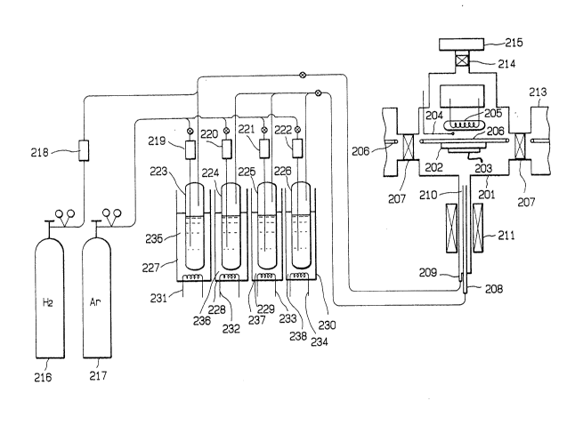
Fig. 2 is a schematic diagram showing the
apparatus for forming a deposited film according to
process (1) of the present invention.
Fig. 3 is a schematic diagram showing the
apparatus for forming a deposited film according to
process ~2) of the present invention.
Fig. 4 is a schematic diagram showing the
apparatus for forming a deposited film according to
process (3) of the present invention~
Fig. 5 is a graph showing the interrelation
between the proportion of crystal grain domains and the
content of hydrogen (H) in the films in Experiments A(2)
and A(3).
Fig. 6 is a graph showing the interrelation
between the content of hydrogen (H) and the change of
conductivity of the films in Experiment B.
Fig. 7 is a graph showing the interrelation
between the content of hydrogen (H) and the drift
mobility of holes of the films in Experiment B.
Fig. 8 is a graph showing the interrelation
between the.....
-- 10 --
.. ~
J ~ 7
the content of hydrogen (H) and the dark conductivity for
films in Experiment C.
Fig. 9 is a graph showing the interrelation between the
content of hydrogen (H) and the proportion of crystal grain
domains for films in Experiment C.
Fig. 10 is a graph showing the interrelation between
the dark conductivity and the flow rate of hydrogen gas at
the time of film formation in Experiment C.
Fig. 11 is a graph showing the interrelation between
the content of hydrogen ~H) and the proportion of crystal
grain domains for films in Experiments D(2) and D~3).
Fig. 12 is a graph showing the interrelation between
the content of hydrogen (H) and the change of conductivity
for films in Experiment E.
Fig. 13 is a graph showing the interrelation between
the content of hydrogen (H) and the drift mobility of holes
for films in Experiment E.
Fig. 14 is a graph showing the interrelation between
the content of hydrogen (H) and the dark conductivity for
films in Experiment F.
Fig. 15 is a graph showing the interrelation between
the content of hydrogen (H) and the proportion of crystal
grain domains for films in Experiment F.
Fig. 16 is a graph showing the interrelation between
the content of hydrogen (H) and the dark conductivity for
1 Jl 1 547
films in Experiment F.
Fig. 17 is a graph showing the interrelation between
the conten-t of hydrogen (l~) and the dark conductivity for
films in Experiment G.
Fig. 18 is a graph showing the interrelation between
the quantitative ratio of Se to Te (Se/Te) and the dark
conductivity for films formed in Experiment G.
Fig. 19 is a graph showing the interrelation between
the content of hydrogen (H) and the dar~ conductivity for
films as formed with the quantitative ratio of Se to Te
(Se/Te) in a p-type doped film being a parameter in
Experiment H.
Fig. 20 is a graph showing the interrelation between
the quantitative ratio of Se to Te (Se/Te) and the dark
conductivity for p-type doped films in Experiment H.
Fig. 21 is a graph showing the interrelation between
the quantitative ratio of Se to Te ~Se/Te) and the dark
conductivity for n-type doped films in Experiment I.
Fig. 22 is a graph showing the interrelation between
the quantitative ratio of Se to Te (Se/Te) and the optical
band gap for films in Experiment J.
Fig. 23 is a graph showing the interrelation between
the quantitative ratio of Se to Te (Se/Te) and the
proportion of crystal grain domains for films in Experiment
K.
- 12 -
1 3 1 1 547
DETAILED DESCRIPTION OF THE INVENTION
The present inventors have made ex-tensive studies for
overcoming the foregoing problems not only on the known ZnSe
film but also on the known ZnSel xTex film for use in
various appliances such as solar cell and attaining the
objects as described above and as a result, have accomplish-
ed the present invention based on the findings obtained
through various experiments as below described.
That is, as a result that there was prepared a ZnSe
deposited amorphous film in which a specific amount of
hydrogen atoms being incorporated and the propor-tion of
crystal grain domains per unit volume being controlled to a
specific value (this deposited film is hereinafter referred
to as "ZnSe:H film"), the present inventors have found the
facts that (a) the ZnSe:H film may be formed in a desired
state even on a non-single crystal substrate of glass,
metal, ceramics or synthetic resin: (b) the ZnSe:H film
formed on such non-single crystal substrate is accompanied
with very few defects: (c) it can be easily and efficiently
doped with a dopant of p-type or n-type: and (d) when doped
with a p-type dopant, there is afforded a desirable p-type
ZnSe:H semiconductor film having a wealth of many
practically applicable semiconductor characteristics.
Then, as a result that there was prepared a ZnSe1 xTex
deposited amorphous film in which the quantitative ratio of
- 13 -
1 -~ 1 1 547
Se to Te was controlled to a specific value, a specific
amount of hydrogen atoms being incorporated and the
proportion of crystal grain domains per unit volume being
controlled to a specific value (this deposited film is
hereinafter referred to as "ZnSe1xTex:H film"), the
present inventors have found that (e) the ZnSe1xTex:H film
may be formed in a desired state even on a non-single
crystal substrate of glass, metal, ceramics or synthetic
resin: (f) the ZnSe1xTex:H film formed on such non-single
crystal substrate is accompanied with very few defects:
(g) it can be easily and efficiently doped with a dopant
of p-type or n-type: and (h) when doped with a p-type
dopant, there is afforded a desirable p-type ZnSe1xTex:H
semiconductor film having a wealth of many practically
applicable semiconductor characteristics.
The present inventors have further found that in
the case of using one or more of the foregoing ZnSe:H
film and the foregoing ZnSe1xTex:H film as a member for
the pin junction in the preparation of a pin junction
photovoltaic element, there is afforded a pin junction
photovoltaic element which efficiently and stably
generates a desired photoelectromotive force.
The present invention has been completed on the
basis of these findings, and it provides pin junction
photovoltaic elements as are below mentioned;
- 14 -
~*
1 3 1 1 547
(1) a pin junction photovoltaic element which generates
photoelectromotive force by the junction of a p-type
semiconductor layer, an i-type semiconductor layer and an
n-type semiconductor layer, characterized in that at
least said i-type semiconductor layer comprises a
deposited film comprised of zinc atoms, selenium atoms
and at least hydrogen atoms: said deposited film contains
said hydrogen atoms in an amount of 1 to 4 atomic %: and
said deposited film contains crystal grain domains in a
proportion of 65 to 85 vol % per unit volume;
(2) the pin junction photovoltaic element as defined in
the above (1), wherein said p-type semiconductor layer
or/and said n-type semiconductor layer comprises a
deposited film comprised of zinc atoms, selenium atoms
and at least hydrogen atoms and which contains a dopant
of p-type or n-type: said deposited film contains said
hydrogen atoms in an amount of 1 to 4 atomic %: and said
deposited film contains crystal grain domains in a
proportion of 65 to 85 vol % per unit volume;
(3) the pin junction photovoltaic element as defined in
the above (2), wherein said p-type dopant is a member
selected from the group consisting of Group I elements
and Group V elements of the Periodic Table;
(4) the pin junction photovoltaic element as defined in
the above (3), wherein said member is lithium;.....
- 15 -
1~1 1547
(5) a pin junction photovoltaic element which generates
photoelectromotive force by the junction of a p-type
semiconductor layer, an i-type semiconductor layer and an
n-type semiconductor layer, characterized in that at
least said i-type semiconductor layer comprises a
deposited film comprised of zinc atoms, selenium atoms,
tellurium atoms and at least hydrogen atoms: the
quantitative ratio of said selenium atoms to said
tellurium atoms in said deposited film is in the range
from 1:9 to 3:7 in terms of number of atoms: said
deposited film contains said hydrogen atoms in an amount
of 1 to 4 atomic %: and said deposited film contains
crystal grain domains in a proportion of 65 to 85 vol %
per unit volume;
(6) the pin junction photovoltaic element as defined in
the above (5), wherein said p-type semiconductor layer
or/and said n-type semiconductor layer comprises a
deposited film comprised of zinc atoms, selenium atoms,
tellurium atoms and at least hydrogen atoms and which
contains a dopant of p-type or n-type: the quantitative
ratio of saicl selenium atoms to said tellurium atoms in
said deposited film is in the range from 1:9 to 3:7 in
terms of number of atoms: said deposited film contains
said hydrogen atoms in an amount of 1 to 4 atomic %: and
said deposited film contains crystal grain domains in a
proportion of 65 to 85 vol % per unit volume;.....
:7~
1 3 1 1 547
(7) the pin junction photovoltaic element as defined in
the above (6), wherein said p-type dopant is a member
selected from the group consisting of Group I elements
and Group V elements of the Periodic Table; and
(8) the pin junction photovoltaic element as defined in
the above (7), wherein said member is lithium.
The experiments carried out by the present
inventors will be detailed in the following.
x~eriment A: Observations on the proportion of crystal
grain domains as formed in a ZnSe
deposited film when hydrogen atoms are
introduced thereinto
(1) Preparation of samples
(i) There were provided two kinds of substances;
(a) a round silicon wafer of 0.5 mm in thickness and 1
inch in diameter (having a resistivity (p) of about
101 n-cm), on which is formed an SiO2 film of about 500 A
in thickness, by way of a known thermal oxidation
treatment in an oxygen gas stream at 1000C and (b) a
square quartz glass of 2.5 cm by 2.5 cm in size.
(ii) The above-mentioned two substrates were
placed side by side on the substrate holder 202 of the
known apparatus as shown in Fig. 2. On every substrate
was formed a ZnSe:H film under the conditions shown in
Table 1. Thus, ......
- 17 -
131 1547
there were prepared samples Nos. 1 - 12 [on substrates (a)]
and samples Nos. 1' - 12' [on substrates (b)].
(iii) Each of samples Nos. 1 - 12 (deposited on
silicon wafers) was cut in half. Each of the cut halves was
cut to a 5 mm square size which matches the holder of th~-
known transmission electron microscope (TEM). The cut piece
r~7 e~su, ~. ~f
was fixed to a glass plate, ~=~.}u}~g 50 mm by 50 mm and 1
mm thick, by the aid of wax, with the deposited film in
contact with the glass surface so that the deposited film is
visible through the opposite wide of the glàss plate.
(iv) The exposed part comprising silicon single
crystal wafer of the sample as prepared in (iii) was etched
with an aqueous solution containing HF, HNO3, and CH3COOH.
The etching rate was properly controlled by changing the
concentration of HF in the etching solution. Etching was
continued until the silicon single crystal wafer was
completely removed. In this case, the progress of etching
was confirmed by observing the light passing through the
deposited film.
(v) After etching, the wax was removed by the aid of an
organic solvent (toluene), and the deposited film was
separated from the glass plate, followed by rinsing and air
drying. Thus there was obtained a film specimen composed of
an SiO2 film and a ZnSe:H film thereon.
~3l 1547
(2) Examination of the film specimens prepared in (1).
Each film specimen of samples Nos. 1-12 formed on
silicon wafers in the above step (1) was examined by
fixing it to the sample holder of the TEM (acceleration
voltage: 200 KeV) to form a transmission image and
observing the resultant transmission image. As a result,
it was found for the resultant transmission image that
there is a lattice image with very few lattice defects in
the part of the ZnSe:H film where crystal grain domains
exist. It was also found that the lattice images are
uniformly distributed throughout the ZnSe:H film.
The lattice image was utilized to determine
crystal grain domains present in a certain area of the
film specimen. Thus the proportion in terms of vol % of
the crystal grain domains present in the deposited film
was calculated.
For reference purposes, the direction of the
crystal grain and the size of the crystal grain domain
were measured by the aid of X-ray diffraction.
(3) Determination of the amount of hydrogen (H) in the
deposited film
(i) each of samples Nos. 1' - 12' deposited on
quartz substrates in the above step (1)-(i) was cut in
half. Each of the cut halves was placed in a vacuum
chamber and heated.....
-- 19 --
1 il 1 547
therein from room temperature to 1000C. During the heating
period, the amount of hydrogen (H) released from the
specimen was determined by means of a mass spectrometer.
The resulting data were compared with those of the standard
sample prepared by implanting a known amount of hydrogen
into a hydrogen-free sample.
(ii) Each deposited film of samples Nos. 1 - 12 used
for the TEM observation was examined for the distribution of
Zn atoms and Se atoms by the aid of an X-ray microanalyzer
("XMA" for short~, made by Shimazu Seisakusho Ltd., and was
also subjected to elemental analysis. The results obtained
were as shown in Table 2.
The data obtained for all of samples Nos. 1 - 12
indicate that Zn atoms and Se atoms are uniformly
distributed in the deposited film, and Zn atoms and Se atoms
constitute the deposited film at a stoichiometric ratio
close to 1:1.
(4) Results
The results of the measurements in the above steps (2)
and (3) are graphically shown in Fig. 5. It was found from
the results shown in Fig. 5 that as the content (atomic%) of
hydrogen atoms (H) in the ZnSe:H film increases, the
proportion of the crystal grain domains per unit volume in
the deposited film decreases. And with the content of
- 20 -
1 Jl 1547
hydrogen atoms in the range of 0.1 to 10 atomic %, the
proportion of crystal grain domains per unit volume in
the film ranges from 90 to 40 vol %.
In the sample preparation in the above step (1),
when the flow rate of hydrogen gas was controlled to a
value lower than 0.05 sccm, the resulting deposited film
became such that it was composed mainly of Zn; and with a
flow rate in excess of 2 slm, no film was deposited.
Experiment B: Observations of the interrelations among
the electrical characteristics, the content of
hydrogen atoms and the proportion of crystal
grain domains per unit volume for the deposited
film
The deposited film formed on the quartz substrate
in the above A-(l)-(ii) was examined for dark
conductivity. The examination was carried out using the
remaining cut halves of samples Nos. 1' - 12'. Prior to
measurements, a comb-shaped aluminum electrode was formed
on each specimen by vacuum deposition. The results
obtained were as shown in Fig. 6.
From the results shown in Fig. 6, the following
was found with respect to the ratio of the change in the
dark conductivity (a) after irradiation with AM-1 light
for 8 hours versus the initial value (~O)~ that is,
~a=a/aO.
That is, it varies depending on the content of
hydrogen......
1 3 1 1 5 ~ 7
atoms (H) in the film. With 4 atomic % or less, almost
no change occurs, and with 8 atomic % or more, a
significant change occurs.
Then, the interrelation between the drift
mobility of holes and the hydrogen content for the
deposited film was examined using the remaining cut
halves of samples Nos. 1 - 12 prepared in the above A-
(1)-(ii). Prior to measurements, each specimen was
provided with an aluminum semitransparent film by vacuum
deposition. The specimen was irradiated with W light
pulses of about 1 nsec while a pulse voltage was being
applied across the aluminum film and the silicon wafer
with the aluminum film being negative. The drift
mobility was measured by way of the known time-of-flight
method. The results obtained were as shown in Fig. 7.
From the results shown in Fig. 7, the following
was found. That is, with a hydrogen content of less than
0.5 atomic %, the drift mobility of holes is very small.
With hydrogen content in the range from 1 to 8 atomic %,
the drift mobility of holes is very high. And with a
hydrogen content in excess of 8 atomic %, the drift
mobility of holes gradually decreases.
These findings suggest that the content of
hydrogen atoms in the deposited film should be 8 atomic %
or less, preferably 4 atomic ~ or less, from the
viewpoint of change in .....
:t
1 3 1 1 5~7
characteristics induced by the irradiation of light, and
0.5 atomic % or more, preferably 1 atomic % or more, from
the viewpoint of the mobility of holes.
As a result of studies shown in Fig. 5, it was
recognized that the proportion of the crystal grain
domains per unit volume is in the range from 65 to 85 vol
% for the deposited film which contains 1 to 4 atomic %
of hydrogen atoms.
It is concluded from the foregoing that the
electrical characteristics of a ZnSe:H deposited film
depend largely on the content of hydrogen atoms (H)
therein and also on the proportion of crystal grain
domains per unit volume therein, and in order for the
deposited film to have desired electrical characteristics
suitable for use in solar cell or in other devices, it is
necessary that the hydrogen content be in the range from
1 to 4 atomic % and the proportion of crystal grain
domains per unit volume be in the range from 65 to 85 vol
%.
Experiment C: Observations of the interrelations among
the doping properties, the content of hydrogen
atoms and the proportion of crystal grain domains
per unit volume for the deposited film
(1) The procedures of Experiment A were
repeated, .....
- 23 -
~c
1 3 t 1 5~7
except that LiC~H7 (1.0 x 10⁻¹ mol/min) was added to the
raw material gas (A) in Table 1, to thereby form a
ZnSe:H:Li deposited film on a silicon wafer (with an sioz
film formed thereon) and on a quartz glass substrate.
Thus there were prepared samples Nos. 13 - 24 (on silicon
wafer) and samples Nos. 13' - 24' (on quartz glass).
(2) Each of samples Nos. 13' - 24' (deposited on
quartz glass substrates) was cut in half. One half was
used for the measurement of dark conductivity after the
formation of a comb-shaped aluminum electrode by vacuum
deposition. The other half was used for the measurement
of the content of hydrogen (H) in the same manner as in
Experiment A.
The results of measurements were as shown in Fig.
8. In the figure, white circles (o) represent the dark
conductivity of the ZnSe:H:Li film which was not
irradiated with light more intense than the room light.
Black circles (-) represent the dark conductivity of the
ZnSe:H:Li film which was measured after continuous
irradiation with AM-1 light (100 mW/Cm2) for 8 hours.
The specimens, with a comb-shaped aluminum
electrode formed thereon by vacuum deposition, were
examined for conductivity type by the aid of
thermoelectromotive force. It was found that the
specimens containing more than 0.25 atomic % of hydrogen
atoms exhibit p-type conductivity, and other specimens
containing less than 0.08 atomic % of ...
- 24 -
~d
1 3 1 1 547
hydrogen atoms exhibit weak n-type conductivity.
(3) Samples Nos. 13 - 24 were examined for the
proportion of crystal grain domains per unit volume in the
same manner as in Experiment A. The results obtained were
as shown in Fig. 9. And it was found that the interrelation
between the proportion of crystal grain domains per unit
volume and the content of hydrogen (H) is almost identical
with that of an undoped film.
(4) From what shown in Figs. 8 and 9, it is recognized
that the film capable of being efficiently doped with a
dopant contains more than 15 vol% of non-crystal grain
domains per unit volume. In other words, for the film to be
doped efficiently, it is necessary that the film be to
contain more than 15 vol~ of non-crystal grain domains per
unit volume.
The foregoing suggests that the deposited film should
contain a certain amount of non-crystal grains. With too
small an amount of non-crystal grains, the resulting
deposited film will be such that lacks in structural
flexibility and is insufficient for structural relief at the
crystal grain boundaries, and because of this, it is
accompanied with defects due to dangling bond for example.
When such film is doped with a proper dopant, the dopant
does not enter the crystal grains but agglomerates at the
crystal grain boundaries. Even though the dopant should be
- 25 -
1 ~ 1 1 547
introduced into the film, the resulting film will be such
that the valence electron and the dark conductivity can not
be controlled as desired.
On the other hand, in the case of a film containing 15
vol% or more of non-crystal grains in the crystal grain
boundaries or in the intercrystal space, with the dangling
bond terminated with hydrogen atoms (H), the structure is
flexible and the defects at the crystal grain boundaries are
few. Therefore, said film is by far superior in the
displacement due to the addition of a dopant, that is, the
doping efficiency to the deposited film which does not
contain non-crystal grain domains. Incidentally, with non-
crystal grain domains being less than 15 vol% per unit
volume, the deposited film is easily peeled off from the
substrate on account of insufficient flexibility in the
structure.
The foregoing suggests that the deposited film should
contain more than 15 vol% of non-crystal grain domains per
unit volume.
(5) The procedures of the above (1) were repeated to
prepare samples Nos. 25 - 36, samples Nos. 37 - 48, and
samples Nos. 49 - 60 (on SiO2 film) and also to prepare
samples Nos. 25' - 36', samples Nos. 37' - 48', and samples
Nos. 49' - 60' (on quartz substrate).
Each of samples Nos. 25 - 60 which were not irradiated
- 26 -
7i 1 1 5~7
n~ense
with ~es~ light was examined for dark conductivity in the
same manner as mentioned above. The results are shown in
Fig. 10. As Fig. 10 illustrates, it was found that the
value of dark conductivity greatly varies depending on the
film forming conditions, and that the degree of variation is
great in the case where the flow rate of hydrogen gas is
high.
On the other hand, as for samples Nos. 25' - 60', it
was found that they are almost uniform in the content of
hydrogen (H) and also in the proportion of crystal grain
domains per unit volume.
In the case of samples Nos. 25' - 60', those which were
prepared with a hydrogen flow rate higher than 30 sccm gave
greatly varied values of dark conductivity. In such cases,
the content of hydrogen (H) was more than 4 atomic% and the
proportion of crystal grain domains per unit volume was less
than 65 vol%.
The foregoing suggests that where the proportion of
non-crystal grain domains per unit volume exceeds 35 vol%,
the crystal grains are electrically separated from one
another and the conduction is determined by the non-crystal
grain domains, which leads to lowering the dark
conductivity. This narrows the application areas of the
resulting deposited film. In addition, the control of
valence electron and the change of dark conductivity with
- 27 -
IJ~ 1547
dopant greatly differ from the crystal grain domains ~o
the non-crystal grain domains; therefore, it is difficult
to obtain the desired control of valence electron and the
desired change of dark conductivity. That is, in the
case where dopants enter the non-crystal grain domains,
but not the crystal grain domains, the resulting
deposited film greatly varies in its characteristics.
This makes it difficult ~o obtain the desired dark
conductivity.
The dark conductivity greatly varies as shown in
Fig. 8 in the case where the deposited film is irradiated
with intense light. This may be elucidated as follows:
In the case where the proportion of the non-crystal grain
domains per unit volume exceeds 35 vol %, the content of
hydrogen (H) is significantly high. This brings about a
situation in which the hydrogen atoms will be easily
released from the film with the progressive lapse of time
and the environmental changes. The release of hydrogen
atoms causes deterioration of the characteristics of the
film.
The foregoing suggests the following. That is,
in order for the ZnSe:H film to be of a stable film
quality and to be reproducible, it is necessary that the
content of hydrogen atoms (H) be 4 atomic % or less and
the proportion of crystal grain domains per unit volume
be 65 vol % or more.
(6) The procedures in the above (1) were repeated
to form ZnSe:H films and ZnSe:H:Li films on quartz
glass.....
- 28 -
.
1 Jll 5 ~ 7
substrates under varied film forming conditions. The
samples thus prepared were examined for the interrelation
between the content of hydrogen (H) and the proportion of
crystal grain domains per unit volume, and the interrelation
between the content of hydrogen ~H) and the electrical
characteristics (such as the ratio of change in conductivity
under irradiation with AM-l light, the drift mobility of
holes, and the dark conductivity) in the same manner as
mentioned above. It was found that the content of hydrogen
(H) and the proportion of crystal grain domains per unit
volume almost coincide with those specified in the above-
mentioned experiments, and that there is a close correlation
between the content of hydrogen (H) in the film and the
electrical characteristics of the film. Thus it was found
that the optimum content of hydrogen (H) is in the range
from 1 to 4 atomic%. It was also found that the proportion
of crystal grain domains per unit volume in the film which
satisfies said specific content of hydrogen (H) in the film
is preferably 65 to 85 vol% and more preferably, 70 to 80
vol%.
- 29 -
1 31 1 547
Experiment D: Observations on the proportion of crystal
grain domains as formed in a ZnSe1 xTex deposited film
when hydrogen atoms are introduced thereinto
(1) Preparation of samples
(i) There were provided two kinds of substrates; (a) a
round silicon wafer of 0.5 mm in thickness and 1 inch in
diameter (having a resistivity (p) of about 10 Q-cm), on
which is formed an SiO~ film of about 5000 A in thickness,
j . a, '`
by way of ~e known thermal oxidation treatment in an oxygen
gas stream at 1000C and (b) a square quartz glass of 2.5 cm
by 2.5 cm in size.
(ii) The above-mentioned two substrates were placed
side by side on the substrate holder 202 of the known
appara~us as shown in Fig. 2. On every substrate was formed
a ZnSel Tex:H film under the conditions shown in Table 3.
Thus, there were obtained samples Nos. 1 - 12 Lon substrates
(a)~ and samples Nos. l' - 12' [on substrates (b)).
(iii) Each of samples Nos. 1 - 12 (deposited on
silicon wafers) was cut in half. Each of the cut halves was
cut to a 5 mm square size which matches the holder of the
known transmission electron microscope (TEM). The cut piece
was fixed to a glass plate, measuring 50 mm by 50 mm and 1
mm thick, by the aid of wax, with the deposited film in
contact with the glass surface so that the deposited film is
visible through -the opposite side of the glass plate.
- 30 -
1 3 i 1 5 4 7
(iv) The exposed part comprising silicon single
crystal wafer of the sample as prepared in (iii) was etched
with an aqueous solution containing HF, HNO3, and CH3COOH.
The etching rate was properly controlled by ~ the
concentration of HF in the etching solution. Etching was
continued until the silicon single crystal wafer was-
completely removed. In this case, the progress of etching
was confirmed by observing the light passing through the
deposited film.
(v) After etching, the wax was removed by the aid of an
organic solvent (toluene), and the deposited film was
separated from the glass plate, followed by rinsing and air
drying. Thus there was obtained a film specimen composed of
an Si2 film and a ZnSel-xTex H film thereon-
(2) Examination of the film specimens prepared in (1)
Each film specimen of samples Nos. 1 - 12 formed on
silicon wafers in the above step (1) was examined by fixing
it to the sample holder of the TEM (acceleration voltage:
200 KeV) to form a transmission image and observing the
resultant transmission image. As a result, it was found for
the resultant transmission image that there is a lattice
image with very few lattice defects in the part of the
ZnSel Tex:H film where crystal grain domains exist. It was
1 3 1 1 547
also found that the lattice images are uniformly
distributed throughout the ZnSelxTex:H film.
The lattice image was utilized to determine
crystal grain domains present in a certain area of the
film specimen. Thus the proportion in terms of vol % of
the cxystal grain domains present in the deposited film
was calculated.
For reference purposes, the direction ~f t~e
crystal grains and the size of the crystal grain domain
were measured by the aid of X-ray diffraction.
(3) Determination of the amount of hydrogen (H) in the
deposited film
(i) Each of samples Nos. 1' - 12' deposited on
quartz substrates in the above-mentioned step (1)-(i) was
cut in half. Each of the cut halves was placed in a
vacuum chamber and heated therein from room temperature
to 1000C. During the heating period, the amount of
hydrogen (H) released from the specimen was determined by
means of a mass spectrometer. The resulting data were
compared with those of the standard sample prepared by
implanting a known amount of hydrogen into a hydrogen-
free sample.
(ii) Each deposited film of samples Nos~ 1 - 12
used for the TEM observations was examined for the
distribution of ........
- 32 -
X
131 15~7
Zn atoms, Se atoms, and Te atoms by the aid of the foregoing
X-ray microanaly~er (XMA) and was also subjected to
elemental analysis. The results obtained were as shown in
Table 4.
The above analysis was carried out on the assumption
that the matrix is comprised of Zn, Se, and Te, and hydrogen
(H) and others in the film were excluded from calculations.
The data obtained for all of samples Nos. 1 - 12
indicate that Zn atoms, Se atoms, and Te atoms are uniformly
distributed in the entire layer region of the deposited film
and that the ratio of Zn atoms versus the sum of Se atoms
and Te atoms is stoichiometrically about 1:1, and the ratio
of Se atoms to Te atoms is 2:8.
(4) Results
The results of the measurements in the above steps (2)
and (3) are graphically shown in Fig. 11. It was found from
the resul.s shown Fig. 11 that as the content (atomic%) of
hydrogen atoms (H) in the ZnSe1 xTex:H film increases, the
proportion of crystal grain domains per unit volume in the
deposited film decreases. And with the content of hydrogen
atoms in the range of 0.1 to 10 atomic%, the proportion of
crystal grain domains per unit volume in the film ranges
from 90 to 40 vol%.
p~epq r~, o n
,,~ In the sample pr~rti~ in the above step (1), when
~31 1547
the flow rate of hydrogen gas was controlled to-a value
lower than 0.05 sccm, the resulting deposited film was
composed mainly of Zn; and with a flow rate in excess of
2 slm, no film was deposited.
Experiment E: Observations on the interrelation among
electrical characteristics, the content of
hydrogen atoms and the proportion of crystal
grain domains per unit volume for the deposited
film
The deposited film formed on the quartz substrate
in the above step (1)-(ii) was examined for dark
conductivity. The examination was carried out using the
remaining cut halves of samples Nos. 1' - 12'. Prior to
measurements, a comb-shaped aluminum electrode was formed
on each specimen by vacuum deposition. The results
obtained were as shown in Fig. 12.
From the results shown in Fig. 12, the following
was found with respect to the ratio of the change in dark
conductivity (a) after irradiation with AM-1.5 for 8
hours versus the initial value (aO), that is, ~a=a/aO.
That is, it varies depending on the content of
hydrogen atoms (H) in the film. With 4 atomic % or less,
almost no change occurs, and with 8 atomic % and above, a
significant change occurs......
- 34 -
`i
1~1 1547
Then, the interrelation between the drift mobility of
holes and the hydrogen content for the deposited film was
examined using the remaining cut halves of samples Nos. 1 -
12 prepared in the above step (1)-(ii). Prior to
measurements, each specimen was provided with an aluminum
semitransparent film by vac-uum deposition. The specimen was
irradiated with UV light pulses of about 1 nsec in a state
that a pulse voltage was being applied across the aluminum
film and the silicon wafer, with the aluminum film being
negative. The drift mobility was measured by way of the
known time-of-flight method. The results obtained were as
shown in Fig. 13.
From the results shown in Fig. 13, the followings were
found. That is, with a hydrogen content of less than 0.5
atomic%, the drift mobility of holes is very small. With a
hydrogen content in the range from 1 to 8 atomic%, the drift
mobility of holes is very high. And with a hydrogen content
in excess of 8 atomic%, the drift mobility of holes
gradually decreases.
These findings suggest that the content of hydrogen
atoms in the cleposited film should be 8 atomic% or less,
preferably 4 atomic% or less, in the viewpoint of change in
characteristics induced by the irradiation of light, and 0.5
atomic% or more preferably 1 atomic% of more, in the
viewpoint of the mobility of holes.
- 35 -
1 7` 1 1 547
As a result of the above-mentioned studies with
due regards to that shown in Fig. 11, it was recognized
that the proportion of the crystal grain domains per unit
volume is in the range from 65 to 85 vol % for the
ZnSe1xTex:H deposited film which contains 1 to 4 atomic %
of hydrogen atoms.
It is concluded from the foregoing that the
electrical characteristics of a ZnSe1xTex:H deposited film
depend largely on the content of hydrogen atoms (H) and
also on the proportion of crystal grain domains per unit
volume in the film, and in order for the deposited film
to have desired electrical characteristics suitable for
use as solar cell or in other devices, it is necessary
that the hydrogen content be in the range from 1 to 4
atomic % and the proportion of crystal grain domains per
unit volume be in the range from 65 to 85 vol ~.
Experiment F: Observations on the interrelations among
the doping properties, the content of hydrogen
atoms and the proportion of crystal grain domains
per unit volume for the deposited film
(1) The procedures in Experiment D were
repeated, except that LiC3H7 (1.0 x 10 10 mol/min) was
added to the raw material gas (A) in Table 3, to thereby
form a........
- 36 -
1 3 1 1 547
ZnSel xTe :H:Li film on a silicon wafer (with an SiO2 film
formed thereon) and also on a quartz glass substrate. Thus
there were prepared samples Nos . 13 - 24 (on silicon wafer)
and samples Nos . 13' - 24' (on quartz glass).
(2) Each of samples Nos . 13' - 24' (deposited on quartz
~ ~7C
glass substrates) was cut in half. ~h~ half was used for
the measurement of dark conductivity after the formation of
a comb-shaped aluminum electrode by vacuum deposition. The
other half was used for the measurement of the content of
hydrogen (H) in the same manner as in Experiment A.
The results of measurements were as shown in Fig. 14.
In the figure, the solid line represents the dark conduc-
tivity of the ZnSe1 xTex:H:Li film which was not irradiated
with light more intense than room light. The broken line
represents the dark conductivity of the ZnSel xTex:H:Li film
which was measured after continuous irradiation with AM-1.5
light (100 mW/cm ) for 8 hours.
The specimens, with a comb-shaped aluminum electrode
formed thereon by vacuum deposition, were examined for
conductivity type by the aid of thermoelectromotive force.
It was found that the specimens containing more than 0.25
atomic ~ of hydrogen atoms exhibit p-type conductivity, and
other specimens containing less than 0.08 atomic ~ of
hydrogen atoms exhibit weak n-type conductivity.
(3) Samples Nos . 13 - 24 were examined for the
1 Jt 1 547
proportion of crystal grain domains per unit volume in the
same manner as in Experiment A. The results obtained were
as shown in Fig. 15. And it was found that the
interrelation between the proportion of crystal grain
domains per unit volume and the content of hydrogen (H) is
almost identical with that of an undoped film.
(4) From what shown in Figs. 14 and 15, it is
recognized that the film capable of being efficiently doped
with a dopant contains more than 15 vol% of non-crystal
grain domains per unit volume. In other words, for the film
to be doped efficiently, it is necessary that the film be to
contain more than 15 vol% of non-crystal grain domains per
unit volume.
The foregoing suggests that the deposited film should
contain a certain amount of non-crystal grains. With too
small an amount of non-crystal grains, the resulting
deposited film will be such that lacks in structural
flexibility and is insufficient structural relief at the
crystal grain boundaries, and because of this, it is
accompanied with defects such as dangling bond. When such
film is doped with a dopant, the dopant does not enter the
crystal grains but agglomerates at the crystal grain
boundaries. Even -though the dopant should be introduced
into the film, the resulting film will be such that the
valence electron and the dark conductivity can not be
controlled as desired.
- 38 -
13l 1547
On the other hand, in the case of a film containing 15
vol% or more of non-crystal grains in the crystal grain
boundaries or in the intercrystal space, with the dangling
bond terminated with hydrogen atoms (H), the structure is
flexible and the defects at the crystal grain boundaries are
few. Therefore, said film is by far superior in the
displacement due to the addition of a dopant, that is the
doping efficiency to the deposited film which does not
contain non-crystal grain domains. Incidentally, with non-
crystal grain domans being less than 15 vol% per unit
volume, the deposited film is easily peeled off from the
substrate on account of its insufficient flexibility in
structure.
The foregoing suggests that the deposited film should
contain more than 15 vol% of non-crystal grain domains per
unit volume.
(5) The procedures of the above (1) were repeated to
prepare samples Nos. 25 - 36, samples Nos. 37 - 48, and
samples Nos. 49 - 60 (on SiO2 film) and also to prepare
samples Nos. 25' - 36', samples Nos. 37' - 48', and samples
Nos. 49' - 60' (on quartz substrate).
Each of samples Nos. 25 - 60 which were not irradiated
with intese light was examined for dark conductivity in the
same manner as mentioned above. The results are shown in
Fig. 16. ~s Fig. 16 illustrates, it was found that the
- 39 -
1~`1 1547
value of dark conductivity greatly varies depending on
the film forming conditions, and that the degree of
variation is great in the case where the flow rate of
hydrogen gas is high.
On the other hand, as for samples Nos. 25'-60' it
was found that they are almost uniform in the content of
hydrogen atoms (H) and also in the proportion of crystal
grain domains per unit volume.
In the case of samples Nos. 25'-60', those which
were prepared with a hydrogen flow rate higher than 30
sccm gave greatly varied values of dark conductivity. In
such cases, the content of hydrogen (H) was more than 4
atomic ~ and the proportion of crystal grain domains per
unit volume was less than 65 vol %.
The foregoing suggests that where the proportion
of non-crystal grain domains per unit volume exceeds 35
vol %, the crystal grains are electrically separated from
one another and the conduction is determined by the non-
crystal grain domains, which leads to a lowering of the
dark conductivity. This narrows the application areas of
the resulting deposited films. In addition, the control
of valence electrons and the change of dark conductivity
with use of a dopant greatly differ from the crystal
grain domains to the non-crystal grain domains;
therefore, it is difficult to obtain the desired control
of valence electrons.....
- 40 -
X
.
4 ~
and the desired change of dark conductivity. That is, in
the case where dopants enter the non-crystal grain
domains, but not the crystal grain domains, the resulting
deposited film greatly varies in its characteristics.
This makes it difficult to obtain the dark conductivity
as desired.
The dark conductivity greatly varies as shown in
Fig. 14 in the case where the deposited film is
irradiated with intense light. This may be elucidated in
the following way: in the case where the proportion of
the non-crystal grain domains per unit volume exceeds 35
vol %, the content of hydrogen (H) is significantly high.
This brings about a situation in which the hydrogen atoms
will be easily released from the film with progressive
change of time and environmental changes. The release of
hydrogen atoms causes deterioration of the
characteristics of the film.
The foregoing suggests the following. That is,
in order for the ZnSe1xTex:H film to be of a stable film
quality and to be reproducible, it is necessary that the
content of hydrogen atom (H) be 4 atomic % or less and
the proportion of the crystal grain domains per unit
volume be 65 vol ~ or more.
(6) The procedures in the above (1) were repeated
to form ZnSe1xTex:H films and ZnSe1xTex:H:Li films on
quartz glass substrates under varied film forming
conditions. Thus prepared samples were examined for the
interrelation between......
- 41 -
131 15~7
the content of hydrogen (H) and the proportion of crystal
grain domains per unit volume, and the interrelation
between the content of hydrogen (H) and the electrical
characteristics (such as the ratio of change in
conductivity under irradiation with AM-1, the drift
mobility of holes, and the dark conductivity) in the same
manner as mentioned above. It was found that the content
of hydrogen (H) and the proportion of crystal grain
domains per unit volume almost coincide with those
specified in the above-mentioned experiments, and that
there is a close correlation between the content of
hydrogen atoms in the film and the electrical
characteristics of the film. Thus it was found that the
optimum content of hydrogen (H) is in the range from 1 to
4 atomic %. It was also found that the proportion of
crystal grain domains per unit volume in the film which
satisfies the specific content of hydrogen atoms in the
film is preferably 65 to 85 vol % and more preferably, 70
to 80 vol %.
Experiment G: Observations on the conductivity of
ZnSe1xTex film in relation to the content of
hydrogen atoms (H) in the film with X (the Se/Te
ratio) as a parameter
(1) Preparation of samples
(i) A square quartz glass of 2.5 cm by 2.5 cm in
size was used as the substrate. .......
- 42 -
~,,
~3~ 1547
(ii) The substrate was firmly attached onto the
substrate holder 202 of the known apparatus as shown in Fig.
2. On the substrate was formed a ZnSel xTex:H film (0<x<1)
under the conditions shown in Table 5. Thus there were
obtained 132 kinds of samples designated by the combination
of two letters L-N, L representing the flow rate of hydrogen
(12 different values) and N representing the ratio of the
flow rate of DESe to the flow rate of DETe (11 different
values).
(2) Determinations of the content of hydrogen (H3 and
the composition ratios of Zn, Se and Te
in the deposited film
(i3 Each of samples Nos. 1-1 - 12-11 deposited on
quartz substrates in the above-mentioned step (l)-(i) was
cut in half. Each of the cut-halves was placed in a vacuum
chamber and heated therein from room temperature to 1000C.
During the heating period, the amount of hydrogen (H)
released from the specimen was determined by means of a mass
spectrometer. The resulting data were compared with those
of the standard sample prepared by implanting a known amount
of hydrogen into a hydrogen-free sample.
(ii) Each of the remaining cut halves of the samples
was examined for the distributions of Zn atoms, Se atoms,
and Te atoms by the aid of an X-ray microanalyzer ("XMA" for
short), made by Shimadzu Seisakusho Ltd., and was also
- 43 -
1 7t 1 547
subjected to elemental composition analysis.
The data obtained indicate that Zn atoms, Se atoms, and
Te atoms are uniformly distributed in the deposited film and
that the ratio of Zn atoms to the sum of Se atoms and Te
atoms [Zn:(Se+Te~ is stoichiometrically about 1:1.
Then, it was confirmed that there may be prepared a
desired ZnSe1 xTex:H deposited film in which the atom number
ratio of Se to Te approximately being (l-x):x by controlling
the flow rate of DESe to 1.5 x lO x (l-x) mol~min. and the
flow rate of DETe to l.0 x lO 5 x x mol/min. respectively.
(3) Measurement of the photoconductivity in relation to
the content of hydrogen (H) for the deposited film
Prior to measurement, there was formed a comb-shaped
electrode (0.2 mm gap) on each of the film samples formed on
quartz glass substrates, which was used for the measurement
in the above (2)-(ii), by the known vacuum deposition
technique.
Then, with lO volts applied under light irradiation
with AM-1.5, a current was measured to examine the
photoconductivity (~p) in relation to the content of
hydrogen (H) for the ZnSel xTex:H deposited film.
The results obtained are shown in terms of the
dependency of the ~p upon the content of hydrogen (H) with
the x being the parameter in Fig. 17. And Fig. 18
illustrates the dependency of the ~p upon the x for the
- 44 -
~3l 1547
ZnSe1xTeK:H deposited films containing 2 atomic % or more
or less than said amount of hydrogen atoms.
These experimental results indicate that there
may be afforded a ZnSe1xTex:H deposited film exhibiting an
outstanding ~p when the content of hydrogen (H) is in the
range from 1 to 10 atomic % and the value of the x is 0.7
< x < O.9, that is, the quantitative ratio of Se to Te is
between 3:7 and 1:9, and said ZnSe1xTex:H deposited film
exhibits desired characteristics suited for use as an i-
type semiconductor layer in a pin type photovoltaic
element.
Experiment H: Observations on the dependency of the dark
conductivity upon the content of hydrogen (H)
with x being the parameter for the p-type doped
ZnSe1xTex:H deposited film
(1) Preparation of samples
There were prepared a predetermined number of
samples by repeating the procedures of Experiment D-(1),
except that LiC3H7 with a flow rate of 1.0 x 10⁻¹ mol/min.
was added to the raw material gas (A~ in Table 5.
(2) Measurements of the content of hydrogen (H) and
compositional ratios of Zn, Se and Te
Each deposited film sample was analyzed to
determine the content of hydrogen (H) and to examine
compositional .......
- 45 -
~r
~. ~
ratios of Zn atoms, Se atoms and Te atoms in the film in the
same manner as in the foregoing Experiment D.
As a result, it was found that Zn atoms, Se atoms and
Te atoms are uniformly distributed in the deposited film and
that the quantitative ratio of Zn atoms to the sum of Se
atoms Te atoms [Zn:(Se+Te)~ is about l:l which satisfies the
stoichiometrical relationship.
Then, it was confirmed that there may be prepared a
desired p-type doped ZnSe1 Tex:H deposited film in which
the atom number ratio of Se to Te being approximately (l-
x):x by controlling the flow rate of DESe to 1.5xlO x(l-x)
mol/min. and the flow rate of DETe to l.OxlO xx mol/min.
respectively.
(3) Measurement of dark conductivity
Every deposited film sample on a quartz glass
substrate, which was used for the measurements in the above
(2), was engaged in examination of the dark conductivity.
Prior to measurement, a comb-shaped aluminum electrode (0.2
mm gap) was formed on said deposited film sample by way of
vacuum deposition. With lO volts applied, a current was
measured in the dark to determin the conductivity (~p) for
the ZnSe1 xTex:H deposited film.
The results obtained are shown in terms of the
dependency of the ~p upon the content of hydrogen (H) with
the x being the parameter in Fig. l9.
- 46 -
13' 15~7
The deposited film samples were examined for conduction
type by way of measuring the thermoelectromotive force. As
a result, it was found that those deposited film samples
containing more than 0.25 atomic % of hydrogen atoms exhibit
p-type conductivity.
Shown in Fig. 20 is of the dependency of the ~p upon
the x for the ZnSel xTex:H deposited films containing 2
atomic % or more or less said amount of hydrogen atoms.
These experimental results indicate that there may be
afforded a desired ZnSel xTex:H deposited film of exhibiting
an excellent p-type conductivity when the content of
hydrogen (H) is in the range from 1 to 10 atomic % and the
value of the x is 0.7 < x < 0.9, that is, the quantitative
ratio of Se to Te is between 1:0 and 9:1 or between 3:7 and
1 : 9 .
Experiment I: Observations on n-type doped ZnSel xTex:H
deposited film
(1) Preparation of samples
There were prepared a predetermined number of samples
by repeating the procedures of Experiment D-(l), except that
(C2H5)3Al~TE al) with a flow rate of 5x10 11 mol/min. was
added to the raw material gas (A) in Table 5.
- 47 -
1 3 1 1 547
(2) Measurements of the content of hydrogen (H) and
compositional ratios of Zn, Se and Te
Every deposited film sample was analyzed to determin
the content of hydrogen (H) and to examin compositional
ratios of Zn atoms, Se atoms and Te atoms in the film in the
same manner as in the foregoing Experiment D~
As a result, it was found that Zn atoms, Se atoms and
Te atoms are uniformly distributed in the deposited film and
that the quantitative ratio of Zn atoms to the sum of Se
atoms and Te atoms ~Zn:~Se~Te)¦ is about 1:1 which satisfy
the stoichiometrical relationship.
Then, it was confirmed that there may be prepared a
desired n-type doped ZnSel xTex:H deposited film in which
the atom number ratio of Se to Te being approximately
(l-x):x by controlling the flow rate of DESe to 1.5xlO x(l-
x) mol/min. and the flow rate of DETe to l.OxlO xx mol/min.
respectively.
(3) Measurement of dark conductivity
Every deposited film sample on a quartz glass
substrate, which was used for the measurements in the above
(2), was engaged in examination of the dark conductivity.
Prior to measurement, a comb-shaped aluminum electrode
(0.2 mm gap) was formed on said deposited film sample by way
of vacuum deposition.
With 10 volts applied, a current was measured in the
- 48 ~
1~1 1547
dark to determln the conductivity (~p) for the n-type doped
ZnSel xTex:H deposited film.
Then, every deposited fiLm sample was examined for
conduction type by way of measuring the thermoelectromotive
force.
The results obtained indicate that all the deposited
film samples are of n-type conduction and that those
deposited film samples containing 1 to 10 atomic % of
hydrogen atoms exhibit an outstanding value of ~p.
In Fig. 21, there are shown the results of examining
the pendency of ~p upon the x for the n-type doped
ZnSe1 xTex:H deposited film containing 2 atomic % of
hydrogen atoms. As Fig. 21 illustrates, it is understood
that there may be afforded a desired n-type doped
ZnSe1 xTex:H deposited film of exhibiting an excellent
conductivity in all the regions for the quantative ratio of
Se to Te.
_ erlment J: Dependency of the optical band gap upon the
quantitative ratio of Se to Te in ZnSel xTex:H
deposited film
(1) Preparation of samples
ZnSel Tex:H films, with the Se:Te quantitative ratio
varied, were prepared on quartz glass substrates in the same
manner as in Experiment G except that the flow rate of
- 49 -
1 3 5l 547
hydrogen gas was fixed at 15 sccm and the doping gas was
not used in Table 5.
(2) Compositional analysis of samples
In accordance with the method in Experiment G-
(2), the samples were examined for the content of
hydrogen (H), distributed states of Zn atoms, Se atoms
and Te atoms and compositional ratios of these atoms. As
a result, it was found for every sample that Zn atoms, Se
atoms and Te atoms are all uniformly distributed in the
film and that the compositional ratio of Zn atoms to the
sum of Se atoms and Te atoms is about l:1, which
satisfies the stoichiometrical relationship.
It was then confirmed that there may be afforded
a desired ZnSe1xTex:H deposited film in which the atomic
ratio of Se to Te is approximately (1-x):x by controlling
the flow rate of DESe to 1.5xlO-5x(1-x) mol/min. and the
flow rate of DETe to l.Ox10-5xx mol/min. respectively.
(3) Measurement of optical band gap
The samples were examined for the variation of
absorption coefficient as a function of the wavelength of
light, using a spectrophotometer. The optical band gap
of each sample was obtained from the absorption edge.
Fig. 22 shows the optical band gap of ZnSe1xTex:H
films (containing 2 atomic % of hydrogen) plotted against
the Se:Te quantitative ratio. It is recognized that in
the case .......
- 50 -
X
l 7J 1 1 547
of films having the Se:Te quantitative ratio greater than
7:3, the optical band gap is in the range from 2.3 to 2.2
eV.
Experiment K: Observations of the proportion of crystal
grain domains formed in non-doped ZnSel xTex:H film
and doped ZnSel_xTex:H:M film (where M denotes a
dopant of p-type or n-type)
(1) Preparation of samples
In the same meanner as in Experiment G, there were
prepared sample films on silicon wafers (with SiO2 film
formed thereon by way of thermal oxidation method) and also
on quartz glass substrates wherein the flow rate of H2 gas
was fixed to 15 SCCM in Table 5.
Incidentally, in the preparation of p-type
ZnSel Te :H:Li films, LiC3~7 was used, and in the prepara-
tion of n-type Znsel-xTex:H:Al films, TEAl [(C2H4)3Al] was
used, respectively while being added to the raw material gas
(A). In the preparation of non-doped ZnSel xTex:H films,
any doping raw material gas was not used.
(2) Analyses of samples
In the same manner as in Experiment D, the resultant
samples were examined for the content of hydrogen (H),
distributed states of Zn atoms, Se atoms and T~ atoms, and
compositional ratios of these atoms.
1 3 t 1 547
As a result, it was found that every sample (deposited
film) contains about 2 atomic% of hydrogen atoms. It was
also found that for any of the samples, Zn atoms, Se atoms
and Te atoms are uniformly distributed in the film and the
compositional ratio of Zn atoms to the sum of Se atoms and
Te atoms is about 1:1 which satisfies the stoichiometrical
relationship.
Then, it was confirmed that there may be afforded a
desired non doped ZnSel xTex:H film or a desired doped
ZnSel xTex:H:M film in which the atom number ratio of Se to
Te being approximately (l-x):x by controlling the flow rate
of DESe to 1.5x10 x(l-x) mol/min. and the flow rate of DETe
to 1.0x10 5xx mol/min. respectively.
(3) Evaluation on the proportion of crystal grain domains
The proportion of crystal grain domains per unit volume
in each sample was evaluated by observing the lattice image
by the foregoing TEM in accordance with the procedures in
Experiment D.
On the basis of the results in the above (2) and (3),
the dependency of the proportion of crystal grain domains
per unit volume upon the x value (the ratio of Te) was
examined for each of the non-doped sample film, the p-type
doped sample film and the n-type doped sample film.
The results obtained are graphically shown in Fig. 23.
The present invention has been completed based on the
I ~' 1 547
foregoing experimental findings.
As mentioned above, one aspect of the present invention
is to provide a pin junction photovoltaic element in which
at least its constituent i-type semiconductor layer
comprises an outstanding functional deposited film
constituted with a material represented by ZnSe:H comprised
of zinc atoms (Zn), selenium atoms (Se) and at least
hydrogen atoms (H), with the content of said hydrogen atoms
being in the range from 1 to 4 atomic % and the proportion
of crystal grain domains per unit volume being in the range
from 65 to 85 vol %.
Another aspect of the present invention is to provide a
pin junction photvoltaic element in which at least its
constituent i-type semiconductor layer comprises an
outstanding functional d~posited film constituted with a
material represented by ZnSel xTex:H comprised of zinc atoms
(Zn), selenium atoms ~Se), tellurium atoms (Te), and at
least hydrogen atoms (H), with the quantitative ratio of
said Se to said Te being between 3:7 and 1:9, the amount of
said H being in the range from 1 to 4 atomic %, and the
proportion of crystal grain domains per unit volume being in
the range from 65 to 85 vol %.
The functional deposited films according to the present
invention mentioned above are expected to find use in broad
application areas. The film may be deposited on a plane or
- 53 -
~3l 1547
cylindrical substrate according to the in-tended applica'cion,
or may also be deposited on a film formed on such substrate.
The ZnSe:H film according to the present invention
contains uniformly distributed Zn atoms and Se atoms in
stoichiometric amounts and also contains hydrogen atoms in
an amount of 1 to 4 atomic% with terminating dangling bonds
of Zn atoms and/or Se atoms or with being present free, and
it contains crystal grain domains and non-crystal grain
domains. The crystal grain domains are uniformly
distributed in the film, and the proportion of the crystal
grain domains per unit volume is in the range from 65 to 85
vol~. Thus the ZnSe:H:M film has excellent uniformity of
structure and homogeneity of composition.
The ZnSel xTe :H fllm according to the present
invention is a deposited film having excellent uniformity of
structure and homogeneity of composition which contains Zn
atoms, Se atoms and Te atoms in stoichiometric amounts
respectively in a state of being uniformly distributed and
also contains 1 to 4 atomic ~ of hydrogen atoms in a state
of terminating dangling bonds of at least one kind of said
Zn, Se and Te atoms or in a state of being present free: the
compositional ratio of said Zn atoms to the sum of said Se
atoms and Te atoms being stoichiometric: the ~uantitative
ratio of said Se atoms to said Te atoms being in the range
from 3:7 to 1:9 in terms of number of atoms: crystal grain
- 54 -
1 3 1 1 5 4 7
domains and non-crystal gra.in domains being contained: and
said crystal grain domains being contained in an amount of
65 to 85 vol % by the proportion per unit volume in a state
of being distributed in the film.
And, any of the ZnSe:H film and the ZnSel xTe :H film
according to the present invention is that the stress to
occur in the entire region is being relaxed in a desired
state, and it has outstanding electrical and mechanical
characteristics and also has good adhesion to the substrate
on which it is to be deposited and other films on or under
which it is to be deposited.
By the way, for the known ZnSe film and ZnSe1 xTe
film, it is difficult to incorporate a dopant thereinto in a
desired state and because of this, it is difficult to make
these film to be of a desired conduction type.
However, according to the present invention, as above
described, any of the foregoing ZnSe:H film and ZnSel xTex:H
film is such that the dangling bounds are being reduced to a
desired low level and that permits easy and effective
incorporation of a dopant thereinto. In view of this,
according to the present invention, there are provided a p-
type ZnSe:H:Mp film and ZnSe1 xTex:H:Mp film (where Mp
represents a p-type dopant). Both films have outstanding p-
type semiconductor characteristics, a desired state in which
the stress is being desirably relaxed as mentioned above,
1 31 1 547
very good electrical and mechanical characteristics, and
good adhesion not only to the substrate but also to other
films.
The ZnSe:H:Mp film and ZnSe1 Tex:H:Mp film contain a
p-type dopant selected from the group consisting of Group IA
elements (i.e., Li, Na, K, and Rb), Group IB elements (i.e.,
Cu and Ag) and Group V-A elements (i.e., P, As, and Sb).
Among these elements, Li and P are most desired.
The amount of the p-type dopant to be contained in the
viewpoint of using the resulting ZnSe:H:Mp film or
ZnSel Tex:H:Mp film as the p-type semiconductor layer in
forming the pin junction is preferably from 50 to lx104
atomic ppm, more preferably from 5X10² to lx104 atomic ppm,
and most preferably, from lxlO to 5xlO atomic ppm.
In addition, according to the present invention, there
are provided an n-type ZnSe:H:Mn film and ZnSe1 xTex:H:Mn
film (where Mn represents an n-type dopant). As well as
said p-type films, these ZnSe:H:Mn film and ZnSe1 xTex:H:Mn
film have outstanding n-type semiconductor characteristics,
a desired state in which the stress is being desirably
relaxed as mentioned above, very good electrical and
mechanical characteristics, and good adhesion not only to
the substrate but also to other films.
As the n-type dopant (Mn), there can be mentioned Group
III B elements such as ~, Al, Ga and In, Group IV B elements
- 56 -
131 1547
such as Si, Ge, C and Sn, and Group VII B elements such as
F, Cl, Br and I. Among these elements, Al, Ga, In and ~ are
most desired.
The amount of the n-type dopant to be contained in the
viewpoint of using the resulting ZnSe:H:Mn film or
ZnSel xTex:H:Mn film as the n-type semiconductor layer in
forming the pin junction is preferably from 50 to lx104
atomic ppm, more preferably from 5X10² to lx104 atomic ppm,
and most preferably, from lx103 to 5x10³ atomic ppm.
As mentioned above, the functional deposited film to be
used in the present invention is characterized by (i) the
content of hydrogen atoms being in the specific range and
~ii) the proportion of crystal grain domains per unit volume
being also in the specific range. As for the hydrogen
content, when it is less than 1 atomic%, the resulting
deposited film becomes unsatisfactory on account of an
excessive amount of dangling bonds. In the case when it
exceeds 4 atomic%, the resulting deposited film becomes also
unsatisfactory because of occurrence of lattic disturbance,
generation of void and also increase of defects. With
respect to the proportion of crystal grain domalns per unit
volume, in the case where it is less than 65 vol%, the
absolute amount of crystal grains being one of the factors
to contribute in promotion of the electrical properties is
reduced. And, in the case where it is in excess of 85 vol%,
- 57 -
1 Jl 1547
crystal grains are directly bonded each other to case
formation of the so-called grain boundaries resulting in
occurrence of defects due to lattice incommensurateness,
etc. Therefore, in any case, there cannot be obtained a
desired deposited film having the characteristics as
desired.
Any of the ZnSe:H film, ZnSe:H:M film, ZnSel xTex:H
film and ZnSe1_xTex:H:M film (where M donates a p-type
dopant or an n-type dopant) to be used in the contains a
specific amount of hydrogen atoms and a specific proportion
of crystal grain domains per unit volume and is specific in
the composition and the structure as above described and
because of this, defects in the film are being significantly
reduced and it is greately surpassing any of the known ZnSe
film, ZnSe:M film, ZnSel xTex film and ZnSel Te :M film
particularly in view of the electrical conductivity. This
situation can be apparently recognized in the case of the
ZnSel Tex:H:Mp -fi~l. That is, as Fig. 20 illustrates, it
is understood that in the case of doping a p-type dopant,
when the value x (the ratio of Te) is in the range of 0< x <
1.0 or in the range of 0.7 < x < 1.0, there is afforded a
large value of the ad (dark conductivity) and the improve-
ment in the doping efficiency is brought about. And as Fig.
23 illustrates, it is understood that when the value x (the
ratio of Te) is in any of the foregoing ranges, the
proportion of crystal grain domains per unit volume stays in
- 58 -
t `'l 1547
the range of more than 65 vol % and the doping efficiency
may be optimized by controlling the aforesaid proportion
with the content of hydrogen atoms. As for the non-doped
ZnSe1xTex:H film, as Fig. 23 illustrates, it is understood
that although the proportion of crystal grain domains per
unit volume is high over the entire range of the value x,
the photoconductivity (~p) is significantly high when the
value x is in the range of 0.7 < x < 0.9 and because of
this, a non-doped ZnSe1xTex:H film in which the value x
(the ratio of Te) is in said range is suitable for use as
the i-type semiconductor layer in the preparation of a
pin junction photovoltaic element.
This situation is considered to be due to that
not only the proportion of crystal grain domains per unit
volume but also the distribution of localized levels in
band gap are changed upon changing the value x.
In addition, as for the foregoing non-doped
ZnSe:H film and non-doped ZnSe1xTex:H films, the band gap
of the former is about 2.67 eV which is effective for the
absorption of short-wavelength light and the band gap of
the latter is from about 2.3 to 2.4 eV which is also
effective for the absorption of short-wavelength light.
This also suggests that any of these films are suitable
for use as the i-type semiconductor layer in the
preparation of a pin junction photovoltaic element having
a high photoelectric conversion efficiency for short-
wavelength light. ........
- 59 -
X,
13t t547
Now, the present invention is to provide a photovoltaic
element of the layer structure having pin junction. The pin
junction is formed so as to provide a high open-circuit
voltage (Voc) using materials respectively having a great
band gap. In the photovoltaic element having the pin
junction, that-is, the pin junction photovoltaic element
according to the present invention, there is used the
foregoing ZnSe:H film or ZnSe1 xTex:H film respectively
having an improved electrical conductivity as its i-type
semiconductor layer, and as its p-type and n-type
semiconductor layers, there are used selected semiconductive
deposited films respectively having more or less around the
same band gap as the i-type semiconductor layer comprising
said ZnSe H film or ZnSe1 xTex H film or ZnScl xTex H film
and which has a good electrical conductivity.
In a preferred embodiment, there is used a member
selected from the foregoing ZnSe:H:M film and inSel xTex:H:M
film as the p-type semiconductor layer or the n-type
semiconductor layer.
In the case where the p-type semiconductor layer is
made of a member selected from the foregoing ZnSe:H:Mp film
and ZnSel xTex:Mp film, the resulting pin junction
photovoltaic element becomes a desired one since any of said
films to constitute the p-type semiconductor layer is of a
wide band gap and has excellent characteristics which are
1 71 1547
hardly found on the known p-type semiconductive deposited
films.
However, as the p-type semiconductor layer or the n-
type semiconductor layer in the pin junction photovoltaic
element according to the present invention, other
semiconductive deposited films having p-type conduction or
n-type conduction than those above mentioned may be
selectively used.
As such semiconductive deposited film having n-type
conduction, there can be mentioned ZnO deposited film, ZnS
deposited film and ZnSe deposited film. And as such
semiconductive deposited film having p-type conduction,
there can be mentioned ZnTe deposited film and CdTe
deposited film. It is a matter of course that these
mentioned deposited films are made n-type or p-type properly
by the addition of a corresponding dopant of n-~ype or p-
type.
Examples of the n-type dopant for the ZnS deposited
film are Cl, Br and Al, and for the ZnSe deposited film are
Br, Ga and Al. Examples of the p-type dopant for the ZnTe
deposited film are Cu, Ag and P, and for the CdTe deposited
film are Li, Sb and P.
The pin junction photovoltaic element according to the
present invention provides a high Voc as well as a high
photoelectric conversion efficiency because of using the
61 -
1 3 1 1 547
foregoing non-doped ZnSe:H film or ZnSel_xTex:H film as the
i-type semiconductor layer in junction with an appropriate
p-type semiconductor layer and an appropriate n-type
semiconductor layer.
The thus structured pin junction photovoltaic element
according to the present invention is high in the
transmission for short-wavelength light and provides
selective absorption and a high photoelectric conversion
efficiency for short-wavelength light mainly because of
using the foregoing non-doped ZnSe:H film or ZnSel xTex:H
film as the i-type semiconductor layer which are free from
problems caused by in-film defects which are found on the
known pin junction photovoltaic element.
This feature makes it possible for the photovoltaic
element according to the present invention to apply to solar
cell where lt achieves more efficient photoelectric
conversion than conventional ones made of amorphous silicon
material even when used under a light source such as white-
light fluorescent lamp which emits such light having a large
quantity of short-wavelength light in its spectral
components. In addition, the photovoltaic element according
to the present invention also exhibits significant effects
when applied to solar cell to be used under sunlight. For
instance, when it is employed as -the cell in the side where
light is impinged in a solar cell of tandem type or triple
- 62 -
t ~1 1 547
type, the resulting device has a structure that permits
efficient transmission of long-wavelength light into the
lower cell and provides a significant improvement in the
photoelectric conversion efficiency for short-wavelength
light. Because of this, it functions to efficiently
convert almost all the spectra of entire sunlight spectra
into electricity. In addition, it can be continuously
used for a long period of time without occurrence of
problems relating to light-induced fatigue which is often
found in the conventional solar cells of tandem type or
triple type.
The following describes typical examples of the
pin junction photovoltaic element to be provided
according to the present invention in which at least the
i-type layer comprises the foregoing ZnSe:H film or the
foregoing ~nSe1xTex:H film.
The following description, however, is not
intended to limit the scope of the present invention.
Fig. l(A) and Fig. l(B) schematically show
typical embodiments of the pin junction photovoltaic
element according to the present invention which has a
layer structure based on the foregoing functional
deposited film containing at least zinc atoms, selenium
atoms and hydroqen atoms.
Fig. l(A) is a schematic cross-sectional view of
a first representative embodiment of the pin
junction......
- 63 -
~b
1 31 1 547
photovoltaic element according to the present invention.
In Fig. l(A), there is shown a pin junction photovoltaic
element 100 having a structure comprising electrode 102,
n-type semiconductor layer 103, i-type semiconductor
layer 104, p-type semiconductor layer 105, transparent
electrode 106 and collecting electrode 107 disposed in
this order on substrate lOlo
In the pin junction photovoltaic element shown in
Fig. l(A), light is impinged from the side of the
transparent electrode 106.
Fig. l(B) is a schematic cross-sectional view of
a second representative embodiment of the pin junction
photovoltaic element according to the present invention.
In Fig. l(B), there is shown a pin junction
photovoltaic element 100 comprising transparent electrode
106, p-type semiconductor layer 105, i-type semiconductor
layer 104, n-type semiconductor layer 103 and electrode
102 being disposed in this order on transmissive
substrate 101. In the pin junction photovoltaic element
shown in Fig. l(B), light is impinged from the side of
the transmissive substrate 101.
For any of the above pin junction photovoltaic
elements shown in Figs. l(A) and Fig. l(B), it is
possible to transpose each of the n-type semiconductor
layer and the p-type semiconductor layer in accordance
with the .....
- 64 -
1 3 ¦ 1 5 4 7
desired use requirements.
Fig. l(C) is a schematic cross-sectional view of
the known pin junction photovoltaic element for
comparative purposes.
In Fig. l(C), there is shown the known pin
junction photovoltaic element 111 comprising electrode
102, n-type A-Si (amorphous silicon) semiconductor layer
108, i-type A-Si (amorphous silicon) semiconductor layer
109, p-type A-Si (amorphous silicon) semiconductor layer
110, transparent electrode 106 and collecting electrode
107 disposed in this order on substrate 101.
In the pin junction photovoltaic element shown in
Fig. l(C), light is impinged from the side of the
transparent electrode 106.
Explanation will be made for the substrate, each
constituent semiconductor layer and each constituent
electrode in the pin junction photovoltaic element of the
present invention.
Substrate
The substrate 101 used in the pin junction
photovoltaic element according to the present invention
may be of single crystal material or non-single crystal
material. It may be electroconductive or electrically
insulating, and it may be transparent or opaque. Usable
as such substrate are, for .......
- 65 -
1 71 1 r
example, Fe, Ni, Cr, A1, Mo, Au, Nb, Ta, V, Ti, Pt, and
Pb and alloys thereof such as brass and stainless steel.
Other than these, there can be mentioned films or sheets
of synthetic resin such as polyester, polyethylene,
polycarbonate, cellulose acetate, polypropylene,
polyvinyl chloride, polyvinylidene chloride, polystyrene,
polyamide, polyimide and the like, and glass or ceramics.
Examples of the substrate comprising a single
crystal material are, for example, wafer-like shaped
members obtained by slicing an appropriate single crystal
of Si, Ge, C, NaCl, KC1, LiF, GaSb, In As, In Sb, GaP,
MgO, CaF2, BaF2, ~-Al203 or the like. The surface of any
of said wafer-like shaped members may be provided with an
epitaxially grown layer of the same constituent(s) as the
member or of a material whose lattice constant is close
to that of the constituent(s) of the member.
The shape of the substrate may be optionally
determined in accordance with the end use purpose.
Examples are plate, belt, drum and suitable like shapes
having a plane or uneven surface. ~he thickness of the
substrate is properly determined so that the layer
structure as the photovoltaic member can be formed as
desired. In the case where flexibility is required for
the photovoltaic element to be prepared, it can be made
as thin as possible within a range capable of
sufficiently providing the functions as the ......
- 66 -
X
131 1547
substra-te. However, the thickness of the substrate is
usually not less than 10 microns from the view points of its
manufacturing and handling conveniences and its strength.
Electrodes
In the photovoltaic element according to the present
invention, an appropriate electrode is optionally used in
accordance with the configuration of the photovoltaic
element to be prepared. As such electrode, there can be
mentioned lower electrode, upper electrode (transparent
electrode) and collecting electrode. Said upper electrode
denotes the one to be placed at the-side through which light
is impinged, and said lower electrode denotes the one to be
placed opposit to the upper electrode through the
semiconductor layers to be arranged between the two
electrodes.
These electrodes will be explained in the following.
(i) Lower electrode
For the pin junction photovoltaic element according to
the present invention, the side through which light is
impinged is determined depending upon whether there is used
a transmissive member or an untransmissive member as the
substrate 101.
In this connection, the position where the lower
- 67 -
131 1547
electrode 102 is to be placed is properly determined by
the kind the substrate 101 to be used. For example, in
the case where an opaque member such as a metal member is
used as the substrate 101, light for the generation of a
photoelectromotive force is impinged from the side of the
transparent electrode 106.
Now, in the case where the pin junction
photovoltaic element is of the configuration as shown in
Fig. l(A), the lower electrode 102 is desired to be
placed between the substrate 101 and the n-type
semiconductor layer 103. In this case, if the substrate
101 is the one which comprises a electroconductive
member, it can function also as the lower electrode.
However, in the case where thP substrate 101 is
electroconductive but is of a high sheet resistance, the
lower electrode may be disposed as a low-resistance
electrode serving to output a current or in order to
heighten the reflectivity of the incident light at the
surface of the substrate 101 so as to make it utilized
more efficiently.
In the case of Fig. l(B), there is used a
transmissive member as the substrate 101 and light is
impinged from the side of the substrate 101. In this
connection, the lower electrode 102 serving to output a
current is placed on the surface of the top semiconductor
layer above the substrate 101. However, in the case
where there is used an electrically insulating member as
the substrate 101 as in the case of Fig.....
- 68 -
X
1 3 1 1 547
l~B), the lower electrode 102 serving to output a current is
placed between the substrate 101 and the n-type
semiconductor layer 103.
The electrode 102 may be a metallic thin film of a
metal selected from the group consisting of Ag, Au, Pt, Ni,
Cr, Cu, Al, Ti, Zn, Mo and W. Said metallic thin film may
be properly formed by way of the known vacuum deposition
technique, electron-beam deposition technique or reactive
sputtering technique. However, due consideration shall be
made for the metallic thin film to be thus formed not to be
a resistant component for the photovoltaic element. In this
respect, the metallic thin film to constitute the electrode
102 is desired to be such that has a sheet resistance of
preferably 50 Q or less, more preferably, 10 Q or less.
In alternative, it is possible to place a diffusion
preventive layer comprising a electroconductive material
such as zinc oxide between the lower electrode 102 and the
n-type semiconductor layer 103. (This is not shown in Figs.
l(A) and l(B).
In the case where such diffusion preventive layer is
placed in the way as above mentioned, the following
advantages will be expected: (a) it prevents the metal
elements constituting the electrode 102 from diffusing into
the n-type semiconductor layer 103; (b) being provided with
a certain resistance value, it prevent the occurrence of
- 69 -
1 3, 1 5 4 7
shorts, which would otherwise occur between the lower
electrode 102 and the transparent electrode 106 through
the semiconductor layers arranged between them due to
pinholes and the like; and (c) it serves to generate
multiple interferences with the thin film and confine the
light as impinged within the photovoltaic element.
(ii) Upper electrode (transparent electrode)
The transparent electrode 106 is desired to have
a light transmittance of more than 85% so that it serves
to make the semiconductor layer efficiently absorb
sunlight or fluorescent light. In addition to this, it
is desired to have a sheet resistance of 100 n or less
from the viewpoint of preventing the internal resistance
of the photovoltaic element from becoming great thereby
impairing the performance.
In view of the above, the transparent electrode
106 is desired to comprise a thin film of a metal oxide
selected from the group consisting of SnO2, In203, ZnO,
CdO, Cd2SnO2 and ITO (In2O3+SnO2) or a semitransparent thin
film of a metal selected from the group consisting of Au,
Al and Cu.
The transparent electrode 106 is disposed on the
p-type semiconductor layer 105 in the case of the
photovoltaic element shown in Fig. l(A), and it is
disposed on the substrate 101 in the case of the
photovoltaic element shown.....
- 70 -
131 1547
in Fig. l~B).
In any of these cases, it is necessary to
constitute the transparent electrode 106 with a thin film
member selected from the foregoing which is good in
adhesion with the layer or the substrate.
The transparent electrode 106 comprising such
thin film may be formed by way of the known resistance
heating deposition technique, electron-beam heating
deposition technique, reactive sputtering techni~ue or
spraying technique.
(iii) Collecting electrode
The collecting electrode 107 in the photo~oltaic
element according to the present invention is disposed on
the transparent electrode 106 for the purpose of reducing
the surface resistance of said transparent electrode.
The collecting electrode 107 is desired to
comprise a metallic thin film of Ag, Cr, Ni, Al, Ag, Au,
Ti, Pt, Cu, Mo, W or an alloy of these metals. It is
possible for the collecting electrode 107 to be
constituted with a member comprising a stacked plurality
of such metallic thin films.
The shape and the area of the collecting
electrode 107 are properly designed so that a sufficient
quantity of light can be received by the semiconductor
layer. ........
- 71 -
X
131 1547
Specifically as for the shape, it is desired to be such
that extends uniformly all over the light receiving face of
the photovoltaic element. A.s for the area, it is desired to
correspond to a 15% or less in a preferred embodiment or a
10% or less in a more preferred embodiment respectively of
said light receiving face.
And the member of constituting the collecting electrode
107 is desired to be such that has a sheet resistance of
preferably 50 Q or less, more preferably, 10 Q or less.
p-type semiconductor layer, i-type semiconductor layer and
n-type semiconductor layer
The pin junction photovoltaic element according to the
present invention is characterized by constituting the i-
type semiconductor layer with the foregoing ZnSe:H deposited
film or the foregoing ZnSel xTex:H deposited film and
because of this, it is surpassing the known pin junction
photovoltaic element.
This situation is more clarified by the experimentally
obtained results in the following.
As the semiconductor material capable of conducting
photoelectric conversion for short-wavelength light having
high energy, there are known semiconductive compounds
comprising Group II and Group VI elements of the Periodic
Table such as ZnS, ZnSe, ZnTe, CdS, CdSe and ZnO (these
1 3 1 1 547
compounds will be hereinafter called "Group II-VI
compound"), each of which having a comparatively wide band
gap. However, any of these Group II-VI compounds is
insufficient in electrical properties as desired thereon
when it is used as the i-type semiconductor layer in a pin
junction photovoltaic element and because of this, it is
difficult to obtain a desirable pin junction photovoltaic
element with the use of any of these Group II-VI compounds
as the i-type semiconductor layer thereof. In addition for
these Group II-VI compounds, it is difficult to provide a p-
type or n-type semiconductor films by doping any of them
with a dopant of p-type or n-type. Further in addition, it
is extremely difficult to obtain a p-type semiconductor film
having a sufficiently wide band gap therefrom.
This situation can be also understood by the following
results obtained through experiments by the present
inventors.
That is, the present inventors tried to prepare (a~ a
pin junction photovoltaic element using a known i-type ZnSe
semiconductor film or a known i-type Znsel-xTex
semiconductor film, a proper n-type semiconductor film and a
proper p-type semiconductor film, and a (b) another pin
junction photovoltaic element using the foregoing i-type
ZnSe:H semiconductor film or the foregoing i-type
ZnSel Tex:H semiconductor film (x-Ø8) respectively
-73 -
131 15~7
according to the present invention, a proper n-type
semiconductor film and a proper p-type semiconductor film.
The photovoltaic elements obtained were evaluated in the
viewpoints of adhesion of the i-type semiconductor layer
with other layer(s) and open-circuit voltage (Voc). And
there were also evaluated for the effects in the cases where
there were used the foregoing p~type ZnSe:H:Mp or
ZnSel xTex:H:Mp semiconductor film or/and the foregoing n-
type ZnSe:H:Mn or ZnSel xTex:H:Mn semiconductor film
respectively according to the present invention.
In every experiment, there was prepared a pin junction
photovoltaic element of the configuration shown in Fig.
l(B). And there were used a quartz glass plate as the
substrate 101, a ITO thin film formed by the reactive
sputtering method as the transparent electrode 106, and a Ag
thin film formed by the known electron-beam heating method
as the electrode 102. As for the known i-type ZnSe and
ZnSel Tex semiconductor films, the known n-type ZnSe, ZnS
and ZnO semiconductor films and the known p-type ZnTe and
CdTe semiconductor films, they were respectively formed by
the known reactive sputtering method.
As for the i-type ZnSe:H and ZnSel xTe :H semiconductor
films, the n-type ZnSe:H:Mn and ZnSel xTex:H:Mn
semiconductor films, and the p-type ZnSe:H:Mp and
ZnSel Te :H:M semiconductor films according to the present
74
131 1547
invention were prepared in accordance with the method
according to the present invention which will be later
described.
As the n-type and p-type dopants in the above n-
type and p-type semiconductor films, those mentioned in
Tables 6~A) and 6tB) were used.
The evaluation results obtained are shown in
Tables 6(A) and 6(B).
As Tables 6~A) and 6(B) illustrate, it is
understood that the pin junction photovoltaic elements in
which the known i-type Group II-VI semiconductor films
were used are mostly not practically usable, except for
one case which is fairly good. On the other hand, it is
understood that any of the pin junction photovoltaic
elements in which the i-type ZnSe:H semiconductor film or
the i-type ZnSe1xTex:H semiconductor film according to the
present invention is used, is satisfactory in all the
evaluation items. And particularly for the pin junction
photovoltaic elements in which in addition to said i-type
semiconductor films, the p-type ZnSe:H:Mp or ZnSe1xTex:H:Mp
semiconductor films and/or the n-type ZnSe:H:Mn or
ZnSe1xTex:H:Mn semiconductor films were used, they are all
excellent in all the evaluation items.
In view of the above and also in view of the
results in the aforementioned Experiments A through K, it
is recognized that the pin junction photovoltaic element
in which the i-type.....
X
1 3 1 1 5~7
semiconductor layer being constituted with the foregoing
ZnSe:~l film or ZnSel xTex:H film having excellent electrical
and mechanical properties is surpassing the known pin ~unc-
tion photovoltaic element in every respects and exhibits an
improved photoelectric conversion efficiency.
Now, as for the preparation of the pin junction
photovoltaic element according to the present invention, it
is desired to continuously carry out the formation process
of the n-type semiconductor layer, the formation process of
the i-type semiconductor layer and the formation process of
the p-type semiconductor layer. To be more specific in this
respect, the three processes are continuously carried out in
the same film deposition apparatus. Alternatively, they are
separately carried out in respective deposition apparatuses
being continuously connected through gate valves. In this
case, the formation of the n-type semiconductor layer on a
substrate is conducted in a first film deposition apparatus,
then the resulting is transferred into a second film
deposition apparatus under vacuum condition and the i-type
semiconductor layer is formed on the previously formed n-
type semiconductor layer therein, and the resulting is
transferred into a third film deposition apparatus under
vacuum condition and the p-type semiconductor layer is
formed on the previously formed n-type semiconductor layer.
In the meantime, any of the foregoing semiconductor
131 1547
films according to the present invention i.e. the i-type
ZnSe:H and ZnSelxTex:H semiconductor films, the p-type
ZnSe:H:Mp and ZnSe1xTex:H:Mp semiconductor films and the n-
type ZnSe:H:Mn and ZnSe1xTex:H:Mn semiconductor films may
be effectively prepared in accordance with one of the
following three processes (1) through (3).
(1) A process for preparing a functional
deposited film comprised of ZnSe:H or ZnSe1xTex:H which
comprises the steps of introducing a Se-containing raw
material gas and hydrogen gas (H2), or further a Te-
containing raw material gas into an activation space
independent of the film-forming space, applying
activation energy to these gases to form a Se-containing
precursor and hydrogen radicals in an atomic state, or
further including a Te-containing precursor, introducing
said precursor(s) and hydrogen radicals into the film-
forming space, simultaneously introducing a Zn-containing
raw material gas into said film-form~ng space, and
causing said gases to chemically react with each other in
the space surrounding the surface of the substrate being
maintained at elevated temperature in said film-forming
space.
(2) A process for preparing a functional
deposited film comprised of ZnSe:H or ZnSe1xTex:H which
comprises the steps of introducing a Se-containing raw
material gas, hydrogen gas (H2), and a Zn-containing gas,
or further a Te-containing raw material gas into the
film-forming space in .....
- 77 -
X
131 1547
which a substrate is arranged and mixing said gases,
applying a high-frequency power to a cathode installed in
said film-forming space to thereby produce plasma in the
reaction space of the film-forming space, and causing
said gases to chemically react with one another through
decomposition, polymerization, radicalization, and
ionization.
(3) A process for preparin~ a functional
deposited film comprised of ZnSe:H or ZnSe1xTex:H which
comprises the steps of introducing Ar gas and H2 gas into
the film-forming space in which a substrate is arranged
and a cathode is arranged opposite to said substrate
while leaving a certain dist nce between them, said
cathode being provided on the surface thereof with a
target of polycrystal ZnSe or polycrystal ZnSe1xTex,
applying a high-frequency power to said cathode to
thereby perform the sputtering of said polycrystal ZnSe
or polycrystal ZnSe1xTex and form a plasma atmosphere
environment in said film-forming space, and causing Se
and Zn (and also Te) in the atomic state emitt2d from the
target and hydrogen in the atomic state formed by the
plasma exitation of the Hz gas to chemically react with
one other in the space surrounding the surface of the
substrate.
The functional deposited film prepared by any of
the above-mentioned three processes (1) to (3) may be
given semiconductor characteristics by the introduction
of a ..~....
- 78 -
131 1547
dopant. Particularly, it is possible to introduce a p-type
dopant into the ZnSe:H film or ZnSel Te :H film. This
makes it possible to provide a ZnSe:H:Mp film or
ZnSel xTex:H:M film having the p-type conductivity. The
doping in this case may be accomplished by introducing a gas
containing a p-type dopant, alone or in combination with
hydrogen gas, into the film-forming space. Needless to say,
it is also possible to prepare an n-type semiconductor from
the ZnSe:H film or ZnSel xTex:H film by using a gas
containing an n-type dopant in the s~me manner as in the
` 5 e~77 . ca r~ d~ or
preparation of p-type se~n-du~tor film.
The above-mentioned processes (1) to (3) of the present
invention will be described in more detail in the following.
Processes (1) and (2)
As the raw material to introduce Zn ("raw material A"
for short), an easily gasifiable alkyl zinc compound
represented by the formula: R-Zn (where R denotes an alkyl
residue having 1 to 4 carbon atoms) is used. Typical
examples of the alkyl zinc compound include dimethyl zinc
(DMZn) and diethyl zinc (DEZn). Being liquid at room
temperature, these organozinc compounds are gasified by
bubbling with an inert gas carrier such as Ar and He at the
time of their use.
- 79 -
t~l 1547
As the raw material to introduce Se ("raw material B"
for short), a gaseous or easily gasifiable hydrogen selenide
(H2Se), selenium halide, or alkyl selenium compound
represented by the formula: R'-Se (where R' denotes an alkyl
residue having 1 to 4 carbon atoms) is used. Preferred
examples of the selenium halide include selenium
hexafluoride. Preferred examples of the alkyl selenium
compound include dimethyl selenium (DMSe~ and diethyl
selenium (DESe).
As the raw material to introduce Te, a gaseous or
easily gasifiable hydrogen telluride (H2Te), tellurium
halide, or alkyl tellurium compound represented by the
formula: R'-Te (where R' denotes an alkyl residue having 1
to 4 carbon atoms) is used. Preferred examples of the
tellurium halide include tellurium hexafluoride. Preferred
examples of the alkyl tellurium compound include dimethyl
tellurium (DMTe) and diethyl tellurium (DETe).
Incidentally, the raw materials to introduce Se and Te
are collectively referred to as "raw material B" herein-
after.
Among the compounds to be the raw material B, those
which are not gaseous but liquid or solid at room
temperature are gasified at the time of their use by
bubbling with an inert carrier gas such as Ar and He, or by
sublimation with heating.
- 80 -
131 t547
In the preparation of the ZnSe:H film or ZnSel xTex:H
film by the process (1) or (2), H2 gas is purposely used.
According to a preferred embodiment of the process (1),
the gaseous raw material B and H2 gas in combination are
introduced into an activation space, where they are excited
with the action of an activation energy to form active
species. In the case of using non-gaseous raw material B,
the activation space may be constructed such that the non-
gaseous raw material B is gasified by the aid of aforesaid
inert gas or H2 gas and the gas thus formed is excited with
the action of an activation energy.
Needless to say, in the process (1), it is possible to
introduce H2 gas alone into a separate activation space
independent of said activation space, where the H2 gas is
excited with the action of an activation energy.
The above activation energy may be discharge energy,
thermal energy, or light energy, or a combination thereof.
The excitation of the raw material B may be
accomplished by the aid of a proper catalyst as well as the
activation energy.
The above-mentioned process (1) or (2) of the present
invention may be practiced in the following manner to
prepare the p--type or n-type ZnSe:H:M film or the p-type or
n-type ZnSel xTex:H:M film. That is, a gaseous raw material
to provide a p-type dopant or n-type dopant ("p-type dopant
- 81 -
1 3 ¦ 1 5 4 7
raw material" or "n-type dopant raw material" for short) is
introduced, alone, or together with the gaseous raw material
A or the gaseous raw material B, or together with H2 gas.
As the p-type dopant raw material, a gaseous or easily
gasifiable compound is used. Examples of the p-type dopant
raw material include organolithium compounds such as propyl
lithium (LiC3H7) and sec-butyl lithium (Li(sec-C4Hg)) which
are liquid at room temperature; and inorganic lithium
compounds such as lithium sulfide (Li2S~ and lithium nitride
(Li3N) which are solid at room temperature. Additional
preferred examples include AsH3, PH3, PzH4~ AsF3, AsC13,
PF5, PF3, PC13, SbH3, and SbF3.
The n-type dopant raw material, like the p-type dopant
raw material, may be a member selected from those compounds
which are gaseous at room temperature or easily gasifiable.
Preferred examples of such compounds include trimethyl
aluminum (Al(CH3)3~, triethyl aluminum (Al(C2H5)3),
trimethyl gallium (Ga(CH3)3), triethyl gallium (Ga(C2H5)3),
trimethyl indium (In(CH3)3), triethyl indium (In(C2H5)3),
diborane (B2H6), monosilane (SiH4), disilane (Si2H6),
monogermane (GeH4), tin hydride (SnH4), methane (CH4),
ethane (C2H6), ethylene (C2H4), acetylene (C2H2), fluorine
(F2~, and chlorine (C12).
In the case where the p-type or n-type dopant raw
ma-terial is liquid at room temperature, it is gasified at
- 82 -
131 15~7
the time of use by bubbling with an inert gas such as Ar or
He or H2 gas as a carrier gas. In the case where the p-type
or n-type dopant raw material is solid at room temperature,
it is gasified at the time of use by sublimation with
heating by the aid of a carrier gas such as Ar and He in a
sublimation furnace.
In the case where the p-type or n-type ZnSe:H:M film or
the p-type or n-type ZnSel Tex:H:M film is prepared by the
above-mentioned process (1), the dopant raw material is
preferably ~ introduced into the activation space together
with the gaseous raw material B and H2 gas.
The above-mentioned process (1) or (2) of the present
invention may be practiced in the following manner to
prepare the ZnSe:H film or ZnSel Tex:H film, the p-type or
n-type ZnSe:H:M film, or the p-type or n-type ZnSel xTex:H:M
film. That is, the substrate is maintained preferably at a
temperature of 50 to 600C, more preferably at a temperature
of 50 to 500C, and most preferably, at a temperature of 100
to ~00C during the film formation process. So long as the
substrate temperature is in the range of 50 to 600C,
usually there is obtained a deposited film in which crystal
grain domains and non-crystal grain domains coexist, wherein
the amount of hydrogen radicals or the flow rate of H2 gas
is changed during the film formation process.
One of the important film forming factors in the
- 83 -
I 31 1 547
above-mentioned process (1) and (2) is the inner pressure
of the film-forming space upon forming the desired film.
And it is preferably from lxlO-4 to 50 Torr, more
preferably from 5x10³ to 10 Torr, and most preferably,
from lxlO 3 to 5 Torr. In practice, the gaseous raw
material A, the gaseous raw material B and hydrogen gas
(H2), and the gaseous dopant (p-type or n-type) raw
material in cases where it is used, are introduced while
being controlled through respective mass flow controllers
at respective flow rates predetermined by the kind of the
semiconductor film to be prepared and while maintaining
the inner pressure of the film-forming space at a value
in the above range.
In the case of the process (1), the gaseous raw
material A and the gaseous raw material B and the
hydrogen radicals in atomic state are introduced into the
film-forming space at a predetermined ratio. Said ratio,
that is, the ratio of the sum of the flow rates for the
two gaseous raw materials versus the flow rate of the
hydrogen radicals, is properly determined by the kinds of
the two raw materials to be used and also the
characteristics desired for the film to be prepared.
However, in general, it is preferably from 1:10 to 1:104,
and more preferably, from 1:25 to 1:103.
Likewise, in the case of the process (2), the
ratio of ......
- 84 -
~ 3~ ~ 541
the sum of the flow rate for the gaseous raw material A
and the flow rate for the gaseous raw material B versus
the flow rate for the hydrogen gas (H2) is determined by
the interrelations among the high fre~uency power to be
applied, the inner pressure of the film-forming space and
the amount of hydrogen atoms to be incorporated into the
film to be prepared. However, in general~ it is
preferably from 1:20 to 1:5x10⁴, and more preferably, from
1:30 to 1:5x10³.
Process (3)
This process is designed to prepare the above-
mentioned ZnSe:H film or ZnSelxTex:H film, the p-type or
n-type ZnSe:H:M film, or the p-type or n-type
ZnSe1xTe:H:M film by means of sputtering, as mentioned
above.
The target to be used is typically polycrystal
ZnSe or polycrystal ZnSe1xTex containing Se and Te in a
desired ratio. It may also be possible to use two
targets of Zn and Se, two targets of ZnSe and ZnTe, or
three targets of Zn, Se, and Te. In the case where the
sputtering is performed by the application of high-
frequency power to the target, it is preferable to form a
gas atmosphere composed of H2 gas and Ar gas and/or He
gas.
In the case of preparing the p-type or n-type
ZnSe:H:M film, or the p-type or n-type ZnSe1xTex:H:M film
n ......
- 85 -
X
1 3 i 1 547
accordance with the process (3), the above sputtering is
performed in a gas atmosphere composed of H2 gas and Ar
gas and/or He gas and also the foregoing gaseous p-type
or n-type dopant raw material.
In the production of the ZnSe:H film or
ZnSe1xTex:H film, the p-type or n-type ZnSe:H:M film, or
the p-type or n-type ZnSe1xTex:H:M film according to
process (3), the important film-forming conditions
include the target-to-substrate distance, the high-
frequency power, the substrate temperature, the inner
pressure, and the gas flow rate. The target-to-substrate
distance may vary depending on the construction and scale
of the equipment used. In general, it is preferably from
20 to lO0 mm, and more preferably, from 40 to 80 mm. The
high-frequency power may vary depending on the type and
size of the target. In general, it i5 preferably from
0.3 to 7 Wlcm2, and most preferably, from 0.8 to 4 W/cm2.
As for the substrate temperature, it is adjusted to the
same range as in the above-mentioned process (l) or (2).
As for the inner pressure at the time of forming the
film, it is preferably from lxlO-s to lxlO-1 Torr, and more
preferably, from lx10-4 to lxlO-2 Torr. The H2 gas and Ar
gas and/or He gas and the gaseous p-type or n-type dopant
raw material are controlled in relation to the amounts of
Zn and Se (or also the amount of Te) in the atomic state
which are emitted from the ......
- 86 -
t ~1 1 547
target during the sputtering. The respective flow rates
of the above gases are controlled by mass flow
controllers such that the gas atmosphere in the reaction
zone of the film-forming space contains a prescribed
amount of hydrogen atoms (H) or a prescribed sum of
hydrogen atoms (H) and dopant (M) (or H+M). In this
case, the film-forming space is evacuated such that the
above mentioned internal pressure is maintained. And it
is desired to establish a certain ratio between the sum
of Zn and Se (and also Te) in atomic state and the amount
of hydrogen atoms (H) or the sum of hydrogen atoms (H)
and dopant (M) (H+M). It is preferably from 102: 1 to
1:103, more preferably from 10:1 to 1:102, and most
preferably, from 5:1 to 1:50. Any of the above-mentioned
processes (1) to (3) may be practised using a suitable
apparatus. Typical examples of such apparatus are shown
in Figs. 2 to 4.
Fig. 2 schematically shows a preferred example of
the apparatus suitable to practice the process (1) of the
present invention. In Fig. 2, there is shown a film
forming chamber 201 in which is installed a substrate
holder 202. There is shown a substrate 203 which is
fixed onto the substrate holder 202. The substrate 203
is heated by radiation from an infrared heater 205, while
being monitored by a temperature monitor 204. The
substrate holder 202 is transferred to the other film
forming chamber .....
- 87 -
X
1 3 1 1 5~7
213 or a load lock chamber 212 through a gate valve 207
by a substrate transfer unit 206. Raw material gas (A)
is introduced into the film forming chamber 201 through
the gas inlet pipe (A) 208. Raw material gas (B) and
hydrogen gas are introduced through the gas inlet pipe
(B) 209. The gases are activated in an activation region
210 by an activation means 211, and then introduced into
the film forming chamber 201.
The activation means may be any means to
decompose, polymerize, radicalize, or ionize raw material
gases (A) and (B) and hydrogen gas by the aid of electric
energy of direct current, high-frequency, or microwave,
or by the aid of light energy, or heat energy, or by the
aid of catalyst, to thereby promote the reactions among
the raw material gases (A) and (B) and hydrogen gas and
also promote the film-forming reactions on the surface of
the substrate.
The gases in the film-forming chamber are
exhausted through a valve 214 by an exhaust pump 215, so
that the pressure in the film-forming chamber is kept at
a prescribed level.
Explanation will be made of an example of the
preparation of the ZnSe:H film of the present invention
using the apparatus shown in Fig. 2.
At first, Se-containing raw material gas (B) such
as DESe and hydrogen gas are fed through the gas inlet
pipe......
- 88 -
~..
1 ~t 1 547
209. The gases are activated in the activation region 210
with the action of activation energy supplied by the
activating means 211. Thus there are formed ~ Se-con-
taining precursor and hydrogen radicals in atomic state.
On the other hand, the Zn-containing raw material gas
(A) such as DEZn entering through the other gas inlet pipe
208 is introduced into the film forming chamber 201 without
being excited by the activating means because the opening of
the gas inlet pipe 208 is located donwstream being apart
from the activation region 210. In the film forming
chamber, the Zn-containing raw material gas (A) reacts with
hydrogen radicals to form a Zn-containing precursor.
Upon introduction into the film-forming chamber, the
Se-containing precursor, Zn-containing precursor, and
hydrogen radicals react with one another to form a ZnSe:H
film containing a desired amount of hydrogen atoms.
It is considered that hydrogen radicals take part also
in the reaction for film deposition on the substrate
surface. That is, the hydrogen radicals function to remove
unnecessary alkyl groups from the deposited film and also to
terminate dan ling bonds in the ZeSe thin film and they are
`ncor~o~te~
ta]con into the film. The activation energy in the
activating region can be brought to the film-forming chamber
for example by increasing the quantity of the activation
energy supplied by the activating means in case where
- 89 -
1 3 1 1 5 4 7
necessary to promote the reaction of the Zn-containing raw
material gas with hydrogen radicals and the reaction of the
Zn-containing precursor with the Se-containing precursor in
the reaction chamber and also to increase the amount of
hydrogen radicals to be supplied. The amount of hydrogen
atoms (H) to be contained in the ZnSe:H film as obtained can
be controlled by properly adjusting the flow rate of
hydrogen gas introduced as a raw material gas, the quantity
of activation energy to be supplied, the inner pressure in
the film-forming chamber, the distance between the
activation region 210 and the opening of the gas inlet pipe
208, and the substrate temperature. The deposited film can
be made p-type or n-type by adding the above-mentioned
dopant raw material to the raw material gas (A) or raw
material gas (B). In the case of preparing ZnSel xTex:H
film, the raw material gas (B) is introduced together with a
Te-containing raw material gas such as DETe into the system.
Fig. 3 schematically shows a preferred example of the
apparatus used to practice the process (2) of the present
invention. When this apparatus is in operation, raw
material gas (A) is introduced through the gas inlet pipe
308, and raw material gas (B) and hydrogen gas are
introduced through the gas inlet pipe 309. These gases are
eventually mixed and they are reacted while being
decomposed, polymerized, radicalized, and ionized in plasma
1J1 1547
generated by high-frequency power applied to the cathode
312 from the high-frequency source 310 through the
matching circuit 311 to thereby form a ZnSe:H thin film
or a ZnSe1xTex:H film on the substrate 303. In the case
of forming said ZnSe1xTex:H film, the raw material gas (A)
is mixed with a Te-containing raw material gas. 8y
feeding the foregoing dopant raw material in the above
case, the resulting deposited film may be p-type or n-
type.
Fig. 4 schematically shows a preferred example of
the apparatus suitable to practice the process (3) of the
present invention. In Fig. 4, there is shown a cathode
412, onto which is attached a target 416 of ZnSe
polycrystal or ZnSe1xTex polycrystal. Ar gas and H2 gas
are introduced through the gas inlet 408 and they are
ionized by plasma generated by high-frequency power
applied to the cathode 412. The resulting Ar ions and H
ions contribute to the sputtering of the target 416.
Thus a ZnSe:H thin film or a ZnSe1xTex:H film is deposited
on the substrate 403. By mixing the Ar gas and Hz gas
with the above-mentioned dopant raw material, the
resulting deposited film may be made p-type or n-type.
-- 91 --
X
1 547
DESCRIPTION OF THE PREFERRED EMBODIMENTS
The photovoltaic element of the present invention
will be descrobed in more detail with reference to the
following examples, which are not intended to restrict the
scope of the invention.
EXAMPLE 1
A pin junction photovoltic element with the con-
figuration shown in Fig. l(A) was prepared using the
deposited film forming apparatus shown in Fig. 2, in
accordance with the above-mentioned process (1).
At first, a stainless steel substrate 101 of 50 mm by
50 mm in size was placed in a known sputtering apparatus
(not shown). The sput,ering apparatus was evacuated to
10 5 Torr or below. On the substrate was deposited an Ag
thin film of about 1000 A in thickness as the lower elec-
trode 102 by sputtering Ag in argon. The substrate was
removed from the sputtering apparatus and then fixed, with
the lower electrode 102 facing downward, onto the sub-
strate holder 202 on the substrate transfer unit 206
installed in the load lock chamber 212. The load lock
chamber 212 was evacuated to 10 5 Torr or below by means
of a vacuum pump (not shown). During evacuation, the
film-forming chamber 201 was evacuated to 10 Torr or
below by means of the vacuum pump 215. When the pressures
- 92 -
1 J I 1 5~7
in the two chambers became almost balanced, the two
chambers were opened and the substrate transfer unit 206
was moved to the film-forming chamber 201.
The substrate was then heated to about 200C by
actuating electric heater 205.
Thereafter, liquid DESe in Dewar's bottle 223 was
gasified by bubbling it with Ar gas from gas reservoir
217 to generate Ar gas saturated with DESe. At that
time, the flow rate of said Ar gas was controlled to 15
SCCN by means of mass flow controller 219.
The resultant Ar gas saturated with DESe was
successively transported into the gas inlet pipe 209
while the flow rate of DESe was controlled to 1.5 x 10⁻⁵
mollmin. At the same time, H2 gas from gas reservoir 216
was introduced into the gas inlet pipe 209 while its flow
rate was controlled to 15 SCCM by means of mass flow
controller 218. Concurrently, DEZn in Dewar's bottle 224
and TEA1 in Dewar's bottle 225 were introduced into the
gas inlet pipe 208 at respective flow rates of 1.0 x 10⁻⁶
mol/min and 3.0 x 10⁻⁹ mol/min in the same manner as in
the case of said DESe. In each of these two cases, the
flow rate of Ar gas was controlled to 5 SCCM.
In the above, the respective flow rates for said
DESe, DEZn and TEA1 were set up by controlling the
respective temperatures of constant......
- 93 -
13t 15~7
temperature waters 235, 236 and 237 contained in constant
temperature water baths 227, 228 and 229 in which the
Dewar's bottles 223, 224 and 225 b~ placed by means of
electric heaters 231, 232 and 233 in said water baths 227,
228 and 229 to thereby adjust the respective temperatures
of the starting raw liquids for said DESe, DEZn and TEAl
to desired temperatures.
With the exhaust valve 214 properly opened, the inner
pressure of the film-forming chamber 201 was kept at 0.5
Torr. Film-forming was started by applying microwave
power (200 W) from the microwave generator 211. After 2
minutes, there was formed an n-type ZnSe:H:Al film 103 on
the substrate 101. The application of microwave power and
the introduction of gases were suspended, and the film-
forming chamber 201 was evacuated to 10 5 Torr or below by
the vacuum pump 215.
The above procedures were repeated, except that the
introduction of TEAl was not conducted, to thereby deposit
an i-type ZnSe:H film 104 on the previously formed n-type
ZnSe:H:Al film 103. The film-forming was continued for 50
minutes.
Then, there was deposited a p-type ZnSe:H:Li film 105
on the previously formed i-type ZnSe:H film 104 by repeat-
in~ the procedures for the formation of said i-type ZnSe:H
film except that liquld LiC3H7 in Dewar's bottle 226 was
- 94 -
t3t 1547
gasified by bubbling it with Ar gas from the gas reservoir
217 to generate Ar gas saturated with LiC3H7, which was
succcEsiJcly transported into the gas inlet pipe 208 at
flow rate of 1.0 x 10 mol/min for the LiC3H7. The flow
rate of said Ar gas in this case was controlled to 5 SCCM.
And the film-forming was continued for 20 minutes.
The above film-forming conditions are shown in Table
7.
Thereafter, the substrate transfer unit 206 was moved
to the load lock chamber 212 through the gate valve 207.
After cooling therein, the substrate 101 on which were
deposited the n-type, i-type and p-type semiconductor
layers was taken out. Then, the substrate was placed in a
known vacuum deposition apparatus, which was evacuated to
Torr or below. On the foregoing p-type ZnSe:H:Li
semiconductor layer 105 on the substrate 101 was deposited
an ITO thin film of about 700 A in thickness in an oxygen
atmosphere with about 1 x 10 Torr. The source of de-
position was a 1:1 (by weight) mixture of In and Sn placed
in a crucible which was heated by the resistance heating
method. The substrate temperature was 175C. In this way
the transparent electrode 106 was formed. After cooling,
the substrate was removed. With a permalloy mask placed
on the transparent electrode 10~, the substrate was placed
in another known vacuum deposition apparatus, which was
- 95 -
~ 'I 1547
evacuated to 1 x 10 Torr or below. A Ag film of about
1.0 ~m in thickness was deposited by the resistance
heating method to forrn the comb-shaped collecting
electrode 107. Thus there was obtained sample No. 1.
The characteristic properties of Sample No. 1 as a
solar cell were evaluated in the following manner.
The open-circuit voltage (Voc) which is produced when
the transparent electrode 106 is irradiated with AM-l
light (100 mW/cm ) was measured. The output which is
produced when the transparent electrode 106 is irradiated
with AM-l light through a 400-nm interference filter was
measured. The change ~n in conversion efficiency that
takes place after irradiation with AM-l light for 10 hours
was measured.
The results of measurements were as shown in Table
16.
Other than the foregoing, there were provided a
silicon single crystal wafer with a SiO2 film formed
thereon by the known thermal oxidation techniqueJand a
quartz glass plate. And there were deposited a ZnSe:H:Al
film as the aforesaid n-type semiconductive layer, a
ZnSe:H film as the aforesaid i-type semiconductor layer
and a ZnSe:H:Li film as the aforesaid p-type semiconductor
layer respectively on said silicon single crystal wafer
and also on said quartz glass place by repeating the
- 96 -
1~1 1547
aforesaid respective procedures for the formation of these
films.
The resultant deposited films were examined for the
content of hydrogen atoms (H) and the proportion of
crystal grain domains per unit volume in accordance with
the procedures of examining them which were employed in
the foregoing Experiments.
The results obtained were as shown in Table 16.
EXAMPLE 2
A pin junction photovoltaic element with the con-
figuration shown in Fig. l(A) was prepared using the film-
forming apparatus shown in Fig. 3, in accordance with the
above-mentioned process (2).
On a stainless steel substrate 101 (303 in Fig. 3)
was deposited an Ag thin film as the lower electrode 102
in the same manner as in Example 1. The substrate 303 was
fixed onto the substrate holder 302. While the inner
pressure in the film-forming chamber 301 was kept at 10 5
Torr or below, the substrate 303 was heated to about 300C
by means of infrared heater 305. The raw material gas A
and raw material gas shown in the column "n-type" of Table
8 were introduced into the film-forming chamber 301
through the gas inlet pipes 308 and 309 respectively,
under the conditions shown in the column "n-type" of Table
- 97 -
8. 1 ,1 1547
With the exhaust valve 314 properly opened, the
inner pressure of the film-forming chamber 301 was kept
at 1.0 Torr. Film-forming was started by applying high-
frequency power (50 W) from the high-frequency (13.56
MHz) generator 310. (The high-frequency generator 310 is
connected to the cathode 312 through the matching circuit
311). After discharging for 6 minutes, there was
deposited an n-type ZnSe:H:Al film 103. The application
of high-frequency power and the introduction of the gases
were suspended, and the film-forming chamber 301 was
evacuated to 10-5 Torr or below. Then, the raw material
gases A and B shown in the column "i-type" of Table 8
were introduced into the film-forming chamber 301.
With the inner pressure kept at 1.0 Torr, high-
frequency power (50 W) was applied from the high-
frequency source 310. After discharging for 30 minutes
under the film-forming conditions shown in the column "i-
type" of Table 8, there was deposited an i-type ZnSe:H
film 104 on the previously formed n-type ZnSe:A1 film
103.
Then, the above procedures were repeated, except
that there were used the raw material gases A and B shown
in the column "p-type" of Table 8 and the respective flow
rates of said raw material gases were controlled to those
mentioned in the column "p-type" of Table 8, to
thereby......
- 9B -
1 ' I 1 547
desposit a p-type ZnSe:H:Li film 105 on the previously
formed i-type ZnSe:H film 104.
The substrate with the deposited films was removed
from the film-forming chamber. On the deposited p-type
film was formed an ITO film of about 700 A in thickness as
the transparent electrode 106 in the same manner as in
Example 1. On the ITO film was formed an Ag thin film as
the collecting electrode 107. Thus there was obtained
Sample No. 2. The characteristic properties of Sample
No. 2 as a solar cell were evaluated in the same manner as
in Example 1. As a result, there were obtained the
results shown in Table 16.
Other than the foregoing, there were provided a
silicon single crystal wafer with a SiO2 film formed
thereon by the known thermal oxidation technique~ and a
quartz glass plate. And there were deposited an n-type
ZnSe:H:Al film as the aforesaid n-type semiconductor
layer, an i-type ZnSe:H film as the aforesaid i-type
semiconductor layer and a p-type ZnSe:H:Li film as the
aforesaid p-type semiconductor layer respectively on said
silicon single crystal wafer and also on said quartz glass
place by repeating the aforesaid respective procedures for
the formation of these films.
The resultant deposited films were examined for the
content of hydrogen atoms (H) and the proportion of
_ 99 _
t 3 ~ 1 547
crystal grain domains per unlt volume in accordance with
the procedures of examining them which were employed in
the foregoing Experiments.
The results obtained were as shown in Table 16.
EXAMPLE 3
A pin junction photovoltaic element with the con-
figuration shown in Fig. l(A) was prepared using the
apparatus shown in Fig. 4. in accordance with the above-
mentioned process (3).
On a stainless steel substrate 101 (403 in Fig. 4)
was deposited the lower electrode 102 comprising Ag in the
same manner as in Example 1. The substrate was fixed onto
the substrate holder 402 on the substrate transfer unit
406 and transferred into the film-forming chamber 401.
The inner pressure in the film-forming chamber 401 was
kept at 10 Torr or below. A ZnSe polycrystal target 416
was placed on cathode 412. The substrate 403 was heated
to about 200C by means of infrared heater 405. The raw
material gases shown in the column "n-type" of Table 9
were introduced at the respective flow rates shown therein
into the film-forming chamber 401 through the gas inlet
pipe 401.
With the exhaust valve 414 properly opened, the inner
pressure of the film-forming chamber 401 was kept at 0.05
Torr. Film-forming was started by applying high-frequency
- 100 -
t 3 i 1 5 4 7
power (300 W). After discharging for 10 minutes, there
was deposited an n-type ZnSe:H:Al film 103. The discharg-
ing and the introduction of the gases were su pended.
e~Ja c~l ~te~
The film-forming chamber was v~o~med to 10 5 Torr or
below, and the raw material gas shown in the column
"i-type" of Table 9 was introduced at the flow rate shown
therein into the film-forming chamber. After discharging
with a 300 W of high-frequency power and with a vacuum of
0.05 Torr for 30 minutes, there was deposited an i-type
ZnSe:H film 104 on the previously formed n-type ZnSe:H:Al
film 103.
Thereafter, the above procedures were repeated,
except that the raw material gases shown in Table 9 were
introduced at the respective flow rates shown therein, to
thereby deposit a p-type ZnSe:H:Li film 105 on the pre-
viously formed i-type ZnSe:H film 104.
On the foregoing p-type ZnSe:H:Li film was formed an
ITO film of about 700 A in thickness as the transparent
electrode 106 and a Ag film as the collecting electrode
107. Thus there was obtained Sample No. 3. The charac-
teristic properties of Sample No. 3 as a solar cell were
evaluated. The results obtained were as shown in Table
16.
Other than the foregoing, there were provided a
silicon single crystal wafer with a SiO2 film formed
- 101 -
1 3 1 1 5 4 7
thereon by the known thermal oxidation technique, and a
quartz glass plate. And there were deposited an n-type
ZnSe:H:~l film as the aforesaid n-type semiconductor
layer, an i-type ZnSe:H film as the aforesaid i-type
semiconductor layer and a p-type Zn~e:H~Li film as the
aforesaid p-type semiconductor layer respectively on said
silicon single crystal wafer and also on said quartz
glass plate by repeating the aforesaid respective
procedures for the formation of these films.
The resultant deposited films were examined for
the content of hydrogen atoms (H) and the proportion of
crystal grain domains per unit volume in accordance with
the procedures of examining them which were employed in
the foregoing Experiments.
The results obtained were as shown in Table 16.
EXAMPLE 4
In the preparation of the pin junction
photovoltaic element of Examples 1 to 3, the n-type, i-
type and p-type semiconductor layers were all prepared in
the same manner utilizing the same film-forming chamber.
However, the manners for forming these layers may be
different one from the other.
This example illustrates the preparation of a pin
junction photovoltaic element in the case where the
forma- ........
- 102 -
x,l
1 3 1 1 547
tions of the n-type and p-type semiconductor layers were
' n c2
carried out ~ e manner different from the manner for
the formation of the i-type semiconductor layer.
In this example, as the film-forming apparatus, there
was used the apparatus shown in Fig. 3 in which the film-
forming chamber 316 comprises the same film-forming
chamber 201 as shown in Fig. 2.
At fir,st, on a stainless steel substrate 101 (303 in
Fig. 3) was deposited an Ag thin Eilm of 3000 A in thick-
ness as the lower electrode 102. The substrate was fixed
onto the substrate holder 302 on the substrate transfer
unit 306 in the film-forming chamber 301. On the sub-
strate was deposited an n-type ZnSe:H:Al film 103 by
repeating the procedures for the formation of the n-type
ZnSe:H:Al film in Example 2. The film-forming chamber 301
was evacuated to 10 Torr or below, and the substrate
transfer unit 306 was moved into the second film-forming
chamber 316 through the gate valve 307. Subsequently, on
the n-type ZnSe:H:Al film was deposited an i-type ZnSe:H
film 104 by repeating the procedures for the formation of
the i-type ZnSe:H film in Example 1.
Then, the substrate transfer unit 306 was returned
into the first film-forming chamber 301 through the gate
valve 307. The procedures for the formation of the p-type
ZnSe:H:Li film in Example 2 were repeated to thereby
- 103 -
1 7 1 1 5~7
deposited a p-type ZnSe:H:Li film 105 on the previously
formed i-type ZnSe:H film.
On the thus formed p-type ZnSe:H:Li film 105 were
formed a transparent electrode 106 comprising an ITO thin
film then a collecting electrode 107 comprising a Ag thin
film respectively in the same manner as in Example 1.
Thus there was obtained Sample No. 4.
The characteristic properties of Sample No. 4 as a
solar cell were evaluated.
The results obtained were as shown in Table 17.
Other than the foregoing, there were provided a
silicon single crystal wafer with a SiO2 film formed
thereon by the known thermal oxidation technique~and a
quartz glass plate. And there were deposited an n-type
ZnSe:H:Al film as the aforesaid n-type semiconductor
layer, an i-type ZnSe:H film as the aforesaid i-type
semiconductor layer and a p-type ZnSe:H:Li film as the
aforesaid p-type semiconductor layer respectively on said
silicon single crystal wafer and also on said quartz glass
place by repeating the aforesaid respective procedures for
the formation of these films.
The resultant deposited films were examined for the
content of hydrogen atoms (H) and the proportion of
crystal grain domains per uni-t volume in accordance with
the procedures of examining them which were employed in
- 104 -
I Jil 5 4 7
the foregoing Experiments.
The results obtained were as shown in Table 17.
EXAMPLE 5
In this example, there were prepared a variety of pin
junction photovoltaic elements (Sample Nos. 5 to 13) with
the configuration shown in Fig. l(A), respectively having
the n-type semiconductor layer comprising an n-type ZnS:Al
film, the i-type semiconductor layer comprising an i-type
ZnSe:H film and the p-type semiconductor layer comprising
a p-type ZnSe:H:Li film.
In the preparation of each sample, there was used a
stainless steel of 50 mm x 50 mm in size as the substrate
101, and on which was formed a Ag thin film as the lower
electrode 102 in the same manner as in Example 1. There-
after, there were successively formed an n-type ZnS:Al
film as the n-type semiconductor layer 103, an i-type
ZnSe:H film as the i-type semiconductor layer 104 and a
p-type ZnSe:H:Li film as the p-type semiconductor layer
105.
The preparation of the n-type semiconductor layer 103
for each sample was carried out by the corresponding pre-
paration method 4, 5 or 6 shown in Table 10.
The preparation of the i-type semiconductor layer 104
for each sample was carried out by the preparation method
- 105 -
1 3 1 1 547
l(method for the formation of the i-type ZnSe:H film in
Example 1), the preparation method 2 (method for the
formation of the i-type ZnSe:H film in Example 2) or the
preparation method 3 (method for the formation of the
i-type ZnSe:H film in Example 3).
The preparation of the p-type semiconductor layer 105
for each sample was carried out by the preparation method
1 (method for the formation of the p-type ZnSe:H:Li film
in Example 1), the preparation method 2 (method for the
formation of the p-type ZnSe:H:Li film in Example 2) or
the preparation method 3 (method for the formation of the
p-type ZnSe:H:Li film in Example 3).
Then, there were successively formed a ITO thin film
as the transparent electrode 106 and a comb-shaped Ag thin
film as the collecting electrode 107 respectively in the
same manner as in Example 1.
In this way, there were obtained photovoltaic element
samples Nos. 5 to 13.
The characteristic properties of each of these
samples as a solar cell were evaluated in the same
evaluation manner as in Example 1.
The results obtained were as shown in Table 18.
Other than the foregoing, there were provided a
silicon single crystal wafer with a SiO2 film formed
thereon by the known thermal oxidation technique and a
- 106 -
t31 15~7
quartz glass plate. And there were deposited an n-type
ZnS:Al film as the aforesaid n-type semiconductor layer,
an i-type ZnSe:H film as the aforesaid i-type semicon-
ductor layer and a p-type ZnSe:H:Li film as the aforesaid
p-type semiconductor layer respectively on said silicon
single crystal wafer and also on said quartz glass place
by repeating the aforesaid respective procedures for the
formation of these films in the preparation of each of the
foregoing photovoltaic element samples Nos. 5 to 13.
The respective resultant deposited films were
examined for the content of hydrogen atoms (H) and the
proportion of crystal grain domains per unit volume in
accordance with the procedures of examining them which
were employed in the foregoing Experiments.
The results obtained were as shown in Table 18.
EXAMPLE 6
In this example, there were prepared a variety of pin
junction photovoltaic elements (Sample Nos. 14 to 22) with
the configuration shown in Fig. l(A), respectively having
the n-type semiconductor layer comprising an n-type ZnO:Al
film, the i-type semiconductor layer comprising an i-type
ZnSe:H film and the p-type semicondl~ctor layer comprising
a p-type ZnSe:H:Li film.
In -the preparation of each sample, there was used a
- 107 -
t 3 ~ 1 5 4 7
stainless steel of 50 mm x 50 mm in size as the substrate
101, and on which was formed a Ag thin film as the lower
electrode 102 in the same manner as in Example 1. There-
after, there were successively formed an n-type ZnO:Al
film as the n-type semiconductor layer 103, an i-type
ZnSe:H film as the i-type semiconductor layer 104 and a
p-type ZnSe:H:Li film as the p-type semiconductor layer
105.
The preparation of the n-type semiconductor layer 103
for each sample was carried out by the corresponding pre-
paration method 7, 8 or 9 shown in Table 11.
The preparation of the i-type semiconductor layer 104
for each sample was carried out by the preparation method
l(method for the formation of the i-type ZnSe:H film in
Example 1), the preparation method 2 (method for the
formation of the i-type ZnSe:H film in Example 2) or the
preparation method 3 (method for the formation of the
i-type ZnSe:H film in Example 3).
The preparation of the p-type semiconductor layer 105
for each sample was carried out by the preparation method
1 (method for the formation of the p-type ZnSe:H:Li film
in Example 1), the preparation method 2 (method for the
formation of the p-type ZnSe:H:Li film in Example 2) or
the preparation method 3 (method for the formation of the
p-type ZnSe:H:Li film in Example 3).
- 108 -
1 ~1 J5~
Then, there were successively formed a ITO thin film
as the transparent electrode 106 and a comb-shaped Ag thin
film as the collecting electrode 107 respectively in the
same manner as in Example 1.
In this way, there were obtained photovoltaic element
samples Nos. 14 to 22.
The characteristic properties of each of these
samples as a solar cell were evaluated in the same
evaluation manner as in Example 1.
The results obtained were as shown in Table 19.
Other than the foregoing, there were provided a
silicon single crystal wafer with a SiO2 film formed
,. ~..~
~,," ~.
thereon by the known thermal oxidation technique~and a
quartz glass plate. And there were deposited an n-type
ZnO:Al film as the aforesaid n-type semiconductor layer,
an i-type ZnSe:H film as the aforesaid i-type semicon-
ductor layer and a p-type ZnSe:H:Li film as the aforesaid
p-type semiconductor layer respectively on said silicon
single crystal wafer and also on said quartz glass place
by repeating the aforesaid respective procedures for the
formation of these films in the preparation of each of the
foregoing photovoltaic element samples Nos. 14 to 22.
The respective resultant deposited films were
examined for the content of hydrogen atoms (H) and the
proportion of crystal grain domains per unit volume in
- 109 -
1 ~1 15~7
accordance with the procedures of examining them which
were employed in the foregoing Experiments.
The results obtained were as shown in Table 19.
EXAMPLE 7
In this example, there were prepared a variety of pin
junction photovoltaic elements (Sample Nos. 23 to 31) with
the configuration shown in Fig. l(A), respectively having
the n-type semiconductor layer comprising an n-type
ZnSe:Al film, the i-type semiconductor layer comprising an
i-type ZnSe:H film and the p-type semiconductor layer
comprising a p-type ZnSe:H:Li film.
In the preparation of each sample, there was used a
stainless steel of 50 mm x 50 mm in size as the substrate
101, and on which was formed a Ag thin film as the lower
electrode 102 in the same manner as in Example 1. There-
after, there were succ~ssively formed an n-type ZnSe:Al
film as the n-type semiconductor layer 103, an i-type
ZnSe:H film as the i-type semiconductor layer 104 and a
p-type ZnSe:H:Li film as the p-type semiconductor layer
105.
The preparation of the n-type semiconductor layer 103
for each sample was carried out by the corresponding pre-
paration method 10, 11 or 12 shown in Table ~2.
The preparation of the i-type semiconductor layer 104
- 110 -
I ~ I 1 547
for each sample was carried out by the preparation method
l(method for the formation of the i-type ZnSe:H film in
Example 1), the preparation method 2 (method for the
formation of the i-type ZnSe:H film in Example 2) or the
preparation method 3 (method for the formation of the
i-type ZnSe:H film in Example 3).
The preparation of the p-type semiconductor layer 105
for each sample was carried out by the preparation method
1 (method for the formation of the p-type ZnSe:H:Li film
in Example 1), the preparation method 2 (method for the
formation of the p-type ZnSe:H:Li film in Example 2) or
the preparation method 3 (method for the formation of the
p-type ZnSe:H:Li film in Example 3).
~: ~ Then, there were successively formed ~ ITO thin film
as the transparent electrode 106 and a comb-shaped Ag thin
film as the collecting electrode 107 respectively in the
same manner as in Example 1.
In this way, there were obtained photovoltaic element
samples Nos. 23 to 31.
The characteristic properties of each of these
samples as a solar cell were evaluated in the same
evaluation manner as in Example 1.
The results obtained were as shown in Table 20.
Other than the foregoing, there were provided a
silicon single crystal wafer with a SiO2 film formed
- 111 -
~31 15~7
~ ? . ~ ~
thereon by the known thermal oxidation technique~and a
quartz glass plate. And there were deposited an n-type
ZnSe:Al film as the aforesaid n-type semiconductor layer,
an i-type ZnSe:H film as the aforesaid i-type semicon-
ductor layer and a p-type ZnSe:H:Li film as the aforesaid
p-type semiconductor layer respectively on said silicon
single crystal wafer and also on said quartz glass place
by repeating the aforesaid respective procedures for the
formation of these films in the preparation of each of the
foregoing photovoltaic element samples Nos. 23 to 31.
The respective resultant deposited films were
examined for the content of hydrogen atoms (H) and the
proportion of crystal grain domains per unit volume in
accordance with the procedures of examining them which
were employed in the foregoing Experiments.
The results obtained were as shown in Table 20.
EXAMPLE 8
In this example, there were prepared a variety of pin
junction photovoltaic elements (Sample Nos. 32 to 40) with
the configuration shown in Fig. l(A), respectively havlng
the n-type semiconductor layer comprising an n-type
ZnSe:H:Al film, the i-type semiconductor layer comprising
an i-type ZnSe:H film and the p-type semiconductor layer
comprising a p-type ZnTe:Li film.
- 112 -
t3~ 1547
In the preparation of each sample, there was used a
stainless steel of 50 mm x 50 mm in size as the substrate
101, and on which was formed a A~ thin film as the lower
electrode 102 in the same manner as in Example 1. There-
after, there were successively formed an n-type ZnSe:H:Al
film as the n-type semiconductor layer 103, an i-type
ZnSe:H film as the i-type semiconductor layer 104 and a p-
type ZnTe:Li film as the p-type semiconductor layer 105.
The preparation of the n-type semiconductor layer 103
for each sample was carried out by the preparation method
1 (method for the formation of the n-type ZnSe:H:Al film
in Example 1,) the preparation method 2 (method for the
formation of the n-type ZnSe:H:Al film in Example 2) or
p/'~pq ra,~
the ~ _a~ = method 3 (method for the formation of the
n-type ZnSe:H:Al film in Example 3).
The preparation of the i-type semiconductor layer 104
for each sample was carried out by the preparation method
l(method for the formation of the i-type ZnSe:H film in
Example 1), the preparation method 2 (method for the
formation of the i-type ZnSe:H film in Example 2) or the
preparation method 3 (method for the formation of the i-
type ZnSe:H film in Example 3).
The preparation of the p-type semiconductor layer 105
for each sample was carried out by the preparation method
13, 14 or 15 shown in Table 13.
- 113 -
~ 1 547
Then, there were successively formed an ITO thin
film as the transparent electrode 106 and a comb-shaped
Ag thin film as the collecting electrode 107 respectively
in the same manner as in Example 1.
In this way, there were obtained photovoltaic
element samples Nos. 32 to 40.
The characteristic properties of each of these
samples as a solar cell were evaluated in the same
evaluation manner as in Example 1.
The results obtained were as shown in Table 21.
Other than the foregoing, there were provided a
silicon single crystal wafer with a sioz film formed
thereon by the known thermal oxidation technique, and a
quartz glass plate. And there were deposited an n-type
ZnSe:H:Al film as the aforesaid n-type semiconductor
layer, an i-type ZnSe:H film as the aforesaid i-type
semi-conductor layer and a p-type ZnTe:Li film as the
aforesaid p-type semiconductor layer respectively on said
silicon single crystal wafer and also on said quartz
glass plate by repeating the aforesaid respective
procedures for the formation of these films in the
preparation of each of the foregoing photovoltaic element
samples Nos. 32 to 40.
The respective resultant deposited films were
examined for the content of hydrogen atoms (H) and the
proportion of crystal grain domains per unit volume in
......
- 114 -
X
1 3 1 1 547
accordance with the procedures of examining them which
were employed in the foregoing Experiments.
The results obtained were as shown in Table 21.
EXAMPLE 9
In this example, there were prepared a variety of pin
junction photovoltaic elements with the configuration
shown in Fig. l(B)LSample Nos. 41 to 44~, having the
p-type semiconductor layer 105 comprising a ZnSe:H:Li
film, the i-type semiconductor layer 104 comprising a
ZnSe:H film and the n-type semiconductor layer 103 com-
prising a member selected from the group consisting of
ZnSe:H:Al film, ZnS:Al film, ZnO:Al film and ZnSe:Al film.
In the preparation of each sample, there was used a
glass plate ~Corning's glass No. 7059 of Corning Glass
~, U.S.A.) of 50 mm x 50 mm in size as the substrate
Qn
101, and on which was formed a ITO thin film of 500 A in
thickness as the transparent electrode 106 in accordance
with the known reactive sputtering method. Thereafter
there was formed a p-type ZnSe:H:Li film as the p-type
semiconductor layer 105 by repeating the procedures for
the formation of the p-type ZnSe:H:Li film in Example 1.
Successively there was formed an i-type ZnSe:H film as the
i-type semiconductor layer 104 by repeating the procedures
for the formation of the ZnSe:H film in Example 1. Then,
- 115 -
t 7~ 1547
there was formed the above-mentioned n-type film as the
n-type semiconductor layer 103 in accordance with the
foregoing preparation method 1, 4, 7 or 10. This situa-
tion is shown in Table 14.
Thereafter, there was formed a Ag thin film of about
500 A in thickness as the electrode 102 in accordance with
the known electron-beam deposition method.
In this way, there were obtained photovoltaic element
samples Nos. 41 to 44.
The characteristic properties of each of these
samples as a solar cell were evaluated in the same
evaluation manner as in Example 1.
The results obtained were as shown in Table 22.
p~l re qo ,`r~
Other than the foregoding, there were provided a
silicon single crystal wafer with a SiO2 film formed
thereon by the known thermal oxidation technique, and a
quartz glass plate. And on the surface of each of them,
there was deposited a film of each constituent layer for
each photovoltaic element sample by repeating the cor-
responding procedures for the formation thereof.
The resultant deposited films were examined for the
- p~o,~o r ~ J d n
content of hydrogen atoms (H) and the propertiGI~- of
crystal grain domains per unit volume in accordance with
the procedures of examining them, which were employed in
the foregoing Experiments.
- 116 -
t3i 1547
The results obtained were as shown in Table 22.
~t ~n
Further, using the aforesaid glass plate with a,ITO
thin film thereon as the transparent electrode 106, there
was formed a p-type ZnTe:Li film as the p-type
semiconductor layer 105 in the same manner as in Example
8, and there were successively formed an i-type ZnSe:H
film as the i-type semiconductor layer 104 and an n-type
ZnSe:H:Al film as the n-type semiconductor layer 103,
respectively in the same manner as in Example 1. Then,
there was formed a Ag thin film as the electrode 102 on
the previously formed n-type semiconductor layer 103 to
thereby obtain another photovoltaic element sample (Sample
No. 45)-
The same evaluations as made for Samples Nos. 41 to44 were made on the resultant Sample No. 45. As a result,
there were obtained the results as shown in Table 22.
- 117 -
t 3~i 1 547
Comparative Example 1
In this comparative example, there were prepared
three kinds of pin junction photovoltaic element samples
(Sample Nos. 46 to 48) by repeating the procedures of
Example 1 except that the flow rate of H2 gas in the case
of forming an i-type ZnSe:H film as the i-type semicon-
ductor layer 104 was controlled to a value shown in Table
15 in each case, in order to investigate any change in the
photovoltaic element's characteristics upon the flow rate
of said H2 gas for incorporating hydrogen atoms (H) into
the i-type ZnSe:H film.
The characteristic properties of each of the
resultant photovoltaic samples Nos. 46 to 48 as a solar
cell were evaluated in the same evaluation manner as in
Example 1.
The results obtained were as shown in Table 23.
Other than the foregoing, there were provided a silicon
single crystal wafer with a SiO2 film formed thereon by
the known thermal oxidation technique, and a quartz glass
plate. And on the surface of each of them, there was
deposited a film of each constituent layer for each
photovoltaic element sample by repeating the corresponding
procedures for the formation thereof.
The resultant deposited films were examined for the
content of hydrogen atoms (H) and the proportion of
- 118 -
t 71 1547
crystal grain domains per unit volume in accordance with
the procedures of examining them, which were employed in
the foregoing Experiments.
The results obtained were as shown in Table 23.
Comparative Example 2
There was prepared a pin junction photovoltaic
element of A-Si:H basis with the configuration shown in
Fig. l(C) in accordance with the glow discharge method
using the apparatus shown in Fig. 3.
On a stainless steel plate of 50 mm x 50 mm in
size as the substrate 101 (303 in Fig. 3), a Ag thin film
of about 1000 A in thickness was deposited as the
electrode 102 by the known sputtering method.
The resultant laminate was fixed, with the
electrode 102 facing downward, onto the substrate holder
302. The film-forming chamber 301 was evacuated to 10-5
Torr or below, and it was kept at 250C by means of the
heater 305. Into the film-forming chamber 301, were
introduced SiH4 gas, H2 gas, and PH3 gas (diluted to 1%
with H2 gas) through the gas inlet 308 from the
corresponding gas reservoirs (not shown) at respective
flow rates of 30 sccm, 40 sccm, and 10 sccm. While the
inner pressure of the film-forming chamber 301 was kept
at 0.5 Torr, discharging was performed by the application
of a high-frequency power (50......
-- 119 --
X
t31 ~5~7
W) for 3 minutes. Thus there was formed an n-type
A-Si:H:P film to be the n-type semiconductor layer 108
The application of high-frequency power and the
introduction of said gasses were suspended, and the film-
forming chamber 301 was evacuated to 10 5 Torr or below.
Into the film-forming charnber 301, were introduced SiH4
gas and H2 gas from the corresponding gas reservoirs at
respective flow rates of 30 sccm and 40 sccm. Discharging
was performed at 0.5 Torr, with 70 W, and for 60 minutes,
in the same manner as mentioned above. Thus there was
formed an i-type A-Si:H film to be the i-type semicon-
ductor layer 109. The discharging and the introduction of
the gasses were suspended, and the film-forming chamber
301 was evacuated to 10 5 Torr or below~ Into the film-
forming chamber 301, were introduced SiH4 gas, H2 gas, and
B2H6 gas (diluted to 1% with H2 gas) from the correspond-
ing gas reservoirs at respective flow rates of 30 sccm,
200 sccm, and 20 sccm. Discharging was performed at 0.6
Torr, with high-frequency 50 W, and for 2 minutes. Thus
there was formed a p-type a-Si:H:B film to be the p-type
semiconductor layer 110. Then, the resultant sample was
taken out from the film-forming chamber 301. And on this
sample were formed the ITO electrode 105 and the Ag
collecting electrode 106 in the same manner as in Example
1. Thus there was obtained a pin junction A-Si
- 120 -
1J1 1547
photovoltaic element sample (Sample No. 49). The
photovoltaic characteristics of this sample were
evaluated in the same evaluation manner as in Example 1.
The results obtained were as shown in Table 23.
Observations on the Evaluation Results Shown in Table 16
to 23
In the aforesaid Tables 16 to 23, with respect to
characteristic properties required for a pin junction
photovoltaic element, there are indicated the followinq
evaluation items: (a) open-circuit voltage (Voc) which is
generated when the element is irradiated with AM-1 light
(100 mW/cmZ), (b) the relative value of the output which
is generated when the element is irradiated with AM-1
light through a 400-nm interference filter versus the
output which is generated when the A-Si pin -junction
photovoltaic element prepared in Comparative Example 2 is
irradiated through the interference filter, and (c) the
change in photoelectric conversion efficiency that takes
place after continuous irradiation with AM-1 light for 10
hours: the change is expressed by ~n/~o, where ~ is the
amount of change in photGelectric conversion efficiency
and ~O is the initial photoelectric conversion efficiency.
.......
- 121 -
~,,
.
I 3 1 1 5~7
In said Tables 16 to 23, there are also shown the
content of hydrogen atoms (H) and the proportion of
crystal grain domains per unit volume in the i-type
ZnSe:H film, which were measured to see if the i-type
ZnSe:H film constituting the photovoltaic element meets
the requirements for the content of hydrogen atoms (H)
and the proportion of crystal grain domains per unit
volume specified in the present invention.
The evaluation results indicate the following.
That is, (i) each of the constituent semiconductor layers
for the pin junction photovoltaic elements obtained in
Examples 1 to 4 i.e. the p-type ZnSe:H:Li films, the i-
type ZnSe:H films and the n-type ZnSe:H:A1 films contains
the specific amount of hydrogen atoms and has the
specific proportion of crystal grain domains per unit
volume, (ii) each of said pin junction photovoltaic
elements has a desired pin junction of said p-type~ i-
type and n-type semiconductor films and it generates a
high open-circuit voltage, ~iii) each of said pin
junction photovoltaic elements generates a higher output
than the conventional A-Si based pin junction
photovoltaic element when irradiated with AM-1 light
through a 400 nm interference filter, and (iv) each of
said pin junction photovoltaic elements exhibits a
desired and stable photoelectric conversion efficiency
even after continuous irradiation.....
- 122 -
l 7~1l 547
with AM-1 light for a long period of time: this means it
has a desired resistance against light-induced fatigue.
In Example 5, there was prepared a pin junction
photovoltaic element comprising an n-type ZnS:A1 film, an
i-type ZnSe:H film and a p-type ZnSe:Li film formed on a
stainless steel substrate. It was comparable to those
obtained in Examples 1 to 4.
In Example 6, there was prepared a pin junction
photovoltaic element comprising an n-type ZnO:A1 film, an
i-type ZnSe:H film and a p-type ZnSe:H:Li film formed on
a stainless steel substrate. It was comparable to those
obtained in Examples 1 to 4.
In Example 7, there was prepared a pin junction
photovoltaic element comprising an n-type ZnSe:A1 film,
an i-type ZnSe:H film and a p-type ZnSe:H:Li film formed
on a stainless steel substrate. It was comparable to
those obtained in Examples 1 to 4.
In Example 8, there was prepared a pin junction
photovoltaic element comprising an n-type ZnSe:H:A1 film,
an i-type ZnSe:H film and a p-type ZnTe:Li film on a
stainless steel substrate. It was comparable to those
obtained in Examples 1 to 4.
In Example 9, using a glass plate as the
substrate, there were prepared a variety of pin junction
photovoltaic elements in which the p-type semiconductor
layer being......
- 123 -
1 71 1547
comprised of a member selected from a p-type ZnTe:Li film
and a p-type ZnSe:H:Li film, i-type semiconductor layer
being comprised of an i-type ZnSe:H film according to the
present invention, and n-type semiconductor layer being
comprised of a member selected from the group consisting
of a ZnSe:H:Li film according to the present invention,
ZnS:Al film, ZnO:Al film or ZnSe:Al film.
Any of the resultant pin junction photovoltaic
element samples was comparable to those obtained in
Examples l to 4.
In Comparative Example l, there were prepared a
plurality of pin junction photovoltaic elements in the
same manner as in Example l, except that the flow rates of
H2 gas to be introduced into the film-forming chamber were
changed in the formation of their i-type semiconductor
layers. And comparative examinations with respect to
photovoltaic element's characteristics were made on the
resultant pin junction photovoltaic elements. The results
indicate that those pin junction photovoltaic elements
having such i-type ZnSe:H semiconductor layer of which
content of hydrogen atoms (H) being outside the specific
range according to the present invention and the propor-
tion of crystal grain domains per unit volume being
outside the specific range according to the present
invention are all inferior to any of the pin junction
- 124 -
13l 15~7
photovoltaic elements obtained in Examples 1 to 9 in any
of the evaluation items.
In Comparative Example 2, a conventional A-Si pin
junction photovoltaic element was prepared as a standard
against which the photovoltaic element of the present
invention is compared. The evaluation results indicate
that it is of a lower open-circuit voltage and is poor in
resistance against light-induced fatigue.
EXAMPLE 10
A pin junction photovoltaic element with the
configuration shown in Fig. l(A) was prepared using the
deposited film-forming apparatus shown in Fig. 2, in
accordance with above-mentioned process (1).
Firstly, a stainless steel of 50 mm by 50 mm in
size as the substrate 101 (203 in Fig. 2) was placed in a
known sputtering apparatus (not shown). The sputtering
apparatus was evacuated to 10-5 Torr or below. On the
substrate 101 was deposited an Ag thin film of about 1000
A in thickness as the lower electrode 102 b~v sputtering
Ag in argon. The substrate was removed from the
sputtering apparatus and then fixed, with the lower
electrode 102 facing downward, onto the substrate holder
202 on the substrate transfer unit 206 installed in the
load lock chamber 212. The load lock chamber 212 was
......
- 125 -
t 1 547
evacuated to 105 Torr or below by means of a vacuum pump
(not shown). During this stage, the film-forming chamber
201 was evacuated to 10-5 Torr or below by means of the
vacuum pump 215. When the pressures in the two chambers
became almost balanced, the two chambers were opened and
the substrate transfer unit 206 was moved to the film-
forming chamber 201.
The substrate was then heated to about 200C by
actuating electric heater 205.
Thereafter, liquid DESe in Dewar's bottle 223 and
liquid DETe in 224 were gasified by bubbling them
respectively with He gas from gas reservoir 217 to
generate He gas saturated with DESe and He gas saturated
with DETe. At that time, the respective flow rates of
said He gas were controlled to 7.5 SCCM by means of mass
flow controller 219.
The resultant He gas saturated with DESe and He
gas saturated with DETe were successively transported
into the gas inlet pipe 209 while the respective flow
rates of DESe and DETe were controlled to 3.0 x 10⁻⁶
mol/min. and 8 x 10⁻⁶ mol/min. respectively. At the same
time, H2 gas from gas reservoir 216 was introduced into
the gas inlet pipe 209 while its flow rate was controlled
to 15 SCCM by means of mass flow controller 218.
Concurrently, DEZn in Dewar's bottle 225 and TEA1 in
Dewar's bottle 226 were....
- 126 -
X
131 ~547
introduced into the gas inlet pipe 208 at respective flow
rates of 1.0 x 10⁻⁵ mol/min. and 3.0 x 10⁻⁹ mol/min. in the
same manner as in the cases of said DESe and said DETe.
In each of these two cases, the flow rate of He gas was
controlled to 5 SCCM.
In the above, the above respective flow rates for
said DESe, DETe, DEZn and TEA1 were set up respectively
by controlling the respective temperatures of constant
temperature waters 235, 236, 237 and 238 contained in
constant temperature water baths 227, 228, 229 and 230 in
which the Dewar's bottles 223, 224, 225 and 226 were
placed, by means of electric heaters 231, 232, 233 and
234 in said water baths 227, 228, 229 and 230 to thereby
adjust the respective temperatures of the starting raw
liquids for said DESe, DETe, DEZn and TEA1 to desired
temperatures.
With the exhaust valve 214 properly opened, the
inner pressure of the film-forming chamber 201 was kept
at 0.5 Torr. Film-forming was started by applying
microwave power (200 W) from the microwave generator 211.
After 2 minutes, there was formed an n-type
ZnSe1xTex:H:Al film 103 on the substrate 101. The
application of microwave power and the introduction of
the gases were suspended, and the film-forming chamber
201 was evacuated to 10-5 Torr or below by the vacuum pump
215......
- 127 -
13~ 1547
The above procedures were repeated, except that
the introduction of TEA1 was not conducted, to thereby
deposit an i-type ZnSe1xTex:H film 104 on the previously
formed n-type film 103. The film-forming was continued
for 50 minutes.
Then, there was deposited a p-type
ZnSe1xTex:H:Li film 105 on the previously formed i-type
film 104 by repeating the procedures for the formation of
said i-type film, except that liquid LiC3H7 in another
Dewar's bottle (not shown) was gasified by bubbling it
with He gas from the gas reservoir 217 to generate He gas
saturated with LiC3H7, which was successively transported
into the gas inlet pipe 208 at a flow rate of 1.0 x 10⁻⁹
mol/min. for the LiC3H7. The flow rate of said He gas in
this case was controlled to 5 SCCM. And the film-forming
was continued for 20 minutes.
The above film-forming conditions are shown in
Table 24.
Thereafter, the substrate transfer unit 206 was
moved to the load lock chamber 212 through the gate valve
207. After cooling therein, the substrate 101 on which
were deposited the n-type, i-type and p-type
semiconductor layers was taken out. Then, the substrate
was placed in a known vacuum deposition apparatus, which
was evacuated to 10-5 Torr or below. On the foregoing p-
type semiconductor.......
- 128 -
t3, 1547
layer 105 on the substrate 101 was deposited an ITO thin
film of about 700 A in thickness in an oxygen atmosphere
with about 1 x 10 Torr. The source of deposition was a
1:1 (by weight) mixture of In and Sn placed in a crucible
which was heated by the resistance heating method. The
substrate temperature was 175C. In this way the trans-
parent electrode 106 was formed. After cooling, the
substrate was removed. With a permalloy mask placed on
the transparent electrode 106, the substrate was placed in
another known vacuum deposition apparatus, which was
evacuated to 1 x 10 Torr or below. A Ag film of about
1.0 ,um in thickness was deposited by the resistance
heating method to form the comb-shaped collecting
electrode 107. Thus there was obtained sample No. 50.
The characteristic properties of Sample No. 50 as a
solar cell were evaluated in the following manner.
The open-circuit voltage (Voc) which is produced when
the transparent electrode 106 is irradiated with AM-1.5
light (100 mW/cm ) was measured. The output which is
generated when the transparent electrode 106 is irradiated
with AM-1.5 light through a 450-nm interference filter was
measured. The change ~ in conversion efficiency ~hat
takes place after irradiation with AM-1.5 light for 10
hours was measured.
The results of measurements were as shown in Table
- 129 -
t31 15~7
35.
Other than the foregoing, there were provided a
silicon single crystal wafer with a SiO2 film formed
thereon by the known thermal oxidation technique and a
quartz glass plate. And there were deposited a
ZnSel Te :H:Al film as the aforesaid n-type semicon-
ductive layer, a ZnSel xTex:H film as the aforesaid i-type
semiconductor layer and a ZnSel Te :H:Li film as the
aforesaid p-type semiconductor layer respectively and
separately on said silicon single crystal wafer and also
on said quartz glass place by repeating the aforesaid
respective procedures for the formation of these films~
The resultant deposited films were examined for the
content of hydrogen atoms (H) and the proportion of
crystal grain domains per unit volume in accordance with
the procedures of examining them which were employed in
the foregoing Experiments.
The results obtained were as shown in Table 35.
EXAMPLE ll
A pin junction photovoltaic element with the
configuration shown in Fig. l(A) was prepared using the
film-forming apparatus shown in Fig. 3, in accordance with
the above-mentioned process (2).
On a stainless steel substrate 101 (303 in Fig. 3)
- 130 -
t ~ L 15~7
was deposited an Ag thin film as the lower electrode 102
in the same manner as in Example 10. The substrate 303
was fixed onto the substrate holder 302. While the inner
pressure in the film-forming chamber 301 was kept at 10
Torr or below, the substrate 303 was heated to about 300C
by means of infrared heater 305. The raw material gas A
and raw material gas B shown in the column "n-type" of
Table 25 were introduced into the film-forming chamber 301
through the gas inlet pipes 308 and 309 respectively,
under the conditions shown in the column "n-type" of Table
25.
With the exhaust valve 314 properly opened, the inner
pressure of the film-forming chamber 301 was kept at 1.0
Torr. Film-forming was started by applying high-frequency
power (50 W) from the high frequency (13.56 MHz) generator
310. (The high-frequency generator 310 is connected to
the cathode 312 through the matching circuit 311.) After
discharging for 30 minutes, there was deposited an n-type
ZnSel Te :H:Al film 103. The application of high-
frequency power and the introduction of the gases were
e ~, ~ Cc~e~
suspended, and the film-forming chamber 301 was vacuumod
to 10 Torr or below. Then, the raw material gases A and
B shown in the column "i-type" of Table 25 were introduced
into the film-forming chamber 301.
With the inner pressure kept at 1.0 Torr, high-
- 131 -
13t t5~7
frequency power (50 W) was applied from the high-
frequency sources 310. After discharging for 30 minutes
under the film-forming conditions shown in the column "i-
type" of Table 25, there was deposited an i-type
ZnSelxTex:H film 104 on the previously formed n-type film
103.
Then, the above procedures were repeated for 2
minutes, except that there were used the raw material
gases A and B shown in the column "p-type" of Table Z5
and the respective flow rates of said raw material gases
were controlled to those mentioned in the column "p-type"
of Table 25, to thereby deposit a p-type ZnSe1xTex:H:Li
film 105 on the previously formed i-type film 104. The
substrate with the deposited films was removed from the
film-forming chamber. On the deposited p-type film 105
was formed an ITO film of about 700 A in thickness as the
transparent electrode 106 in the same manner as in
Example 10. On the ITO film was formed an Ag thin film
as the collecting electrode 107. Thus there was obtained
Sample No. 51. The characteristic properties of Sample
No. 51 as a solar cell were evaluated in the same manner
as in Example 10. As a result, there were obtained the
results shown in Table 35.
Other than the foregoing, there were provided a
silicon single crystal wafer with a sio2 film formed
thereon by the known thermal oxidation technique, and
a....
~ 132 -
131 1547
quartz glass plate. And there were deposited an n-type
ZnSel Tex:H:Al film as the aforesaid n-type semiconductor
layer, an i-type ZnSel_ Tex:H film as the aforesaid i-type
semiconductor layer and a p-type ZnSel xTe :H:Li film as
the aforesaid p-type semiconductor layer respectively and
separately on said silicon single crystal wafer and also
on said quartz glass place by repeating the aforesaid
respective procedures for the formation of these films.
The resultant deposited films were examined for the
content of hydrogen atoms (H) and the proportion of
crystal grain domains per unit volume in accordance with
the procedures of examining them which were employed in
the foregoing Experiments.
The results obtained were as shown in Table 35.
EXAMPLE 12
A pin junction photovoltaic element with the
configuration shown in Fig. l(A) was prepared using the
apparatus shown in Fig. 4, in accordance with the above-
mentioned process (3).
On a stainless steel substrate 101 (403 in Fig. 4)
was deposited the lower electrode 102 comprising Ag in the
same manner as in Example 1. The substrate was fixed onto
the substrate holder 402 on the substrate transfer unit
406 and transferred into the film-forming chamber 401.
- 133 -
" 1 7i 1547
The inner pressure in the film-forming chamber 401 was
kept at 10-5 Torr or below. A ZnSe1xTex polycrystal target
416 was placed on cathode 412. The substrate 403 was
heated to about 200C by means of infrared heater 405.
The raw material gases shown in the column "n-type" of
Table 26 were introduced at the respective flow rates
shown therein into the film-forming chamber 401 through
the gas inlet pipe 401.
With the exhaust valve 414 properly opened, the
inner pressure of the film-forming chamber 401 was kept
at 0.05 Torr. Film-forming was started by applying high-
frequency power (300 W). After discharging for 3
minutes, there was deposited an n-type ZnSez1xTex:H:Al
film 103. The discharging and the introduction of the
gases were suspended.
The film-forming chamber was evacuated to 10-5
Torr or below, and the raw material gas shown in the
column "i-type" of Table 26 was introduced at the flow
rate shown therein into the film-forming chamber. After
discharging with 300 W of high-frequency power and a
vacuum of 0.05 Torr for 60 minutes, there was deposited
an i-type ZnSe1xTex:H film 104 on the previously formed n-
type film 103.
Thereafter, the above procedures were repeated,
except that the raw material gases shown in Table 26 were
introduced at the respective flow rates shown therein,
to.....
- 134 -
1 3 , 1 5 4 7
thereby deposit a p-type ZnSel xTex:H:Li film 105 on the
previously formed i-type film 10~.
On the foregoi.ng p-type film was formed an ITO film
of about 700 A in thickness as the transparent electrode
106 and a Ag film as the collecting electrode 106. Thus
there was obtained Sample No. 52. The characteristic
properties of Sample No. 52 as a solar cell were
evaluated.
The results obtained were as shown in Table 35.
Other than the foregoing, there were provided a
silicon single cry.~tal wafer with a SiO2 film formed
t~/7~
thereon by ~-e known thermal oxidation technique~and a
~uartz glass plate. And there were deposited an n-type
ZnSel_xTex:H:Al film as the aforesaid n-type semiconductor
layer, an i-type ZnSe1 xTex:H film as the aforesaid i-type
semiconductor layer and a p-type ZnSe1 xTe :H:Li film as
the aforesaid p-type semiconductor layer respectively and
separately on said silicon single crystal wafer and also
on said quartz glass place by repeating the aforesaid
respective procedures for the formation of these films.
The resultant deposited films were examined for the
content of hydrogen atoms (H) and the proportion of
cyrstal grain domains per unit volume in accordance with
the procedures of examining them which were employed in
the foregoing Experiments.
- 135 -
t3~ 1547
The results obtained were as shown in Table 35.
EXAMPLE 13
In the preparation of the pin junction photovoltaic
element in any case of Examples 10 to 12, the p-type, i-
type and p-type semiconductor layers were all prepared
respectively in the same manner utilizing the same film-
forming chamber. However, the manners for forming these
layers may be different one from the other.
This example illustrates the preparation of a pin
junction photovoltaic element in the case where the
formations of the n-type and p-type semiconductor layers
were carried out ~y ~e manner different from the manner
for the formation of the i-type semiconductor layer.
In this example, as the film-forming apparatus, there
was used the apparatus shown in Fig. 3 in which the film-
forming chamber 316 comprises the same film-forming
chamber 201 as shown in Fig. 2.
At first, on a stainless steel substrate 101 ~303 in
Fig. 3) was deposited an Ag thin film of about 3000 A in
thickness as the lower electrode 102. The substrate was
fixed onto the substrate holder 302 on the substrate
transfer unit 306 in the film-fonning chamber 301. On the
substrate was deposited an n-type ZnSel xTex:H:Al film 103
by repeating the procedures for the formation of the n-
- 136 -
I, i 1 5 4 7
type ZnSe1xTex:H:Al film in Example 2. The film-forming
chamber 301 was evacuated to 10-5 Torr or below, and the
substrate transfer unit 306 was moved into the second
film-forming chamber 316 through the gate valve 307.
Subsequently, on the n-type ZnSe1xTex:H:Al film was
deposited an i-type ZnSe1xTex:H film 104 by repeating the
procedures for the formation of the i-type ZnSe1xTex:H
film in Example 1.
Then, the substrate transfer unit 306 was
returned into the first film-forming chamber 301 through
the gate valve 307. The procedures for the formation of
the p-type ZnSe1xTex:H:Li film in Example 2 were repeated
to thereby deposit a p-type ZnSe1xTex:H:Li film 105 on the
previously formed i-type ZnSe1xTex:H film-
On the thus formed p-type ZnSe1xTex:H:Li film 105
were formed a transparent electrode 106 comprising an ITO
thin film and then a collecting electrode 107 comprising
an Ag thin film in the same manner as in Example 10.
Thus there was obtained Sample No. 53.
The characteristic properties of Sample No. 53 as
a solar cell were evaluated in the same evaluation manner
as in Example 10.
The results obtained were as shown in Table 36.
Other than the foregoing, there were provided
a.....
- 137 -
1 71 15~7
silicon single crystal wafer with a SiO2 film formed
thereon by the known thermal oxidation technique and a
quartz glass plate. And there were deposited an n-type
ZnSel Te :H:Al film as the aforesaid n-type semiconductor
layer, an i-type ZnSel xTex:H film as the aforesaid i-type
semiconductor layer and a p-type ZnSel Te :H:Li film as
the aforesaid p-type semiconductor layer respectively and
separately on said silicon single crystal wafer and also
on said ~uartz glass place by repeating the aforesaid
respective procedures for the formation of these films.
The resultant deposited films were examined for the
content of hydrogen atoms (H) and the proportion of
crystal grain domains per unit volume in accordance with
the procedures of examining them which were employed in
the foregoing Experiments.
The results obtained were as shown in Table 36.
EXAMPLE 14
In this example, there were prepared a variety of pin
junction photovoltaic elements (Sample Nos. 54 to 62) with
the configuration shown in Fig. l~A), respectively having
the n-type semiconductor layer comprising an n-type ZnS:Al
film, the i-type semiconductor layer comprising an i-type
ZnSel xI'ex:H film and the p-type semiconductor layer
comprising a p-type ZnSel Te :H:Li film.
- 138 -
1 3 1 1 547
In the preparation of each sample, there was used a
stainless steel of 50 mm x 50 mm in size as the substrate
101, and on which was formed a Ag thin film as the lower
electrode 102 in the same manner as in Example 1. There-
after, there were successively formed an n-type ZnS:Al film
as the n-type semiconductor layer 103, an i-type
ZnSel Tex:H film as the i-type semiconductor layer 104 and
a p-type ZnSel xTex:H:Li film as the p-type semiconductor
layer 105.
The preparation of the n-type semiconductor layer 103
for each sample was carried out by the corresponding pre-
paration method 19, 20 or 21 shown in Table 27.
The preparation of the i-type semiconductor layer 104
for each sample was carried out by the preparation method 16
(method for the formation of the i-type ZnSel xTex:H film in
Example 10), the preparation method 17 (method for the
formation of the i-type ZnSel xTex:H film in Example 11) or
the preparation method 18 (method for the formation of the
i-type ZnSel xTex:H film in Example 12).
The preparation of the p-type semiconductor layer 105
for each sample was carried out by the preparation method
16 (method for the formation of the p-type ZnSel xTe :H:Li
film in Example 10), the preparation method 17 (method for
the formation of the p-type ZnSel_xTex:H:Li film in
Example 11) or the preparation method 18 (method for the
- 139 -
1 31 1 547
formation of the p-type ZnSel_xTe :H:Li film in Example
12).
Then, there were successively formed a ITO thin film
as the transparent electrode 106 and a comb-shaped~ Ag
thin film as the collecting electrode 107 respectively in
the same manner as in Example 10.
In this way, there were obtained photovoltaic element
samples Nos. 54 to 62.
The characteristic properties of each of these
samples as a solar cell were evaluated in the same evalua-
tion manner as in Example 10.
The results obtained were as shown in Table 37.
Other than the foregoing, there were provide a
silicon single crystal wafer with a SiO2 film formed
thereon by the known thermal oxidation technique~ and a
quartz glass plate. And there were deposited an n-type
ZnS:Al film as the aforesaid n-type semiconductor layer,
an i-type ZnSel Tex:H film as the aforesaid i-type semi-
conductor layer and a p-type ZnSel xTex:H:Li film as the
aforesaid p-type semiconductor layer respectively and
separately on said silicon single crystal wafer and also
on said quartz glass place by repeating the aforesaid
respective procedures for the formation of these films in
the preparation of each of the foregoing photovoltaic
element samples Nos. 54 to 62.
- 140 -
131 1547
The respective resultant deposited films were
examined for the content of hydrogen atoms (H) and the
proportion of crystal grain domains per unit volume in
accordance with the procedures of examining them which
were employed in the foregoing Experiments.
The results obtained were as shown in Table 37.
- 141 -
13t ~547
EXAMPLE 15
In this example, there were prepared a variety of pin
junction photovoltaic elements (Sample Nos. 63 to 71) with
the configuration shown in Fig. l(A), respectively having
the n-type semiconductor layer comprising an n-type ZnO:Al
film, the i-type semiconductor layer comprising an i-type
ZnSel Tex:H film and the p-type semiconductor layer
comprising a p-type ZnSel xTex:H:Li film.
In the preparation of each sample, there was used a
stainless steel of 50 mm x 50 mm in size as the substrate
101, and on which was formed a Ag thin film as the lower
electrode 102 in the same manner as in Example 10. There-
after, there were successively formed an n-type znotAl film
as the n-type semiconductor layer 103, an i-type
ZnSel xTex:H film as the i-type semiconductor layer 104 and
a p-type ZnSel xTex:H:Li film as the p-type semiconductor
layer 105.
The preparation of the n-type semiconductor layer 103
for each sample was carried out by the corresponding pre-
paration method 22, 23 or 24 shown in Table 28.
The preparation of the i-type semiconductor layer 104.
for each sample was carried out by the preparation method 16
(method for the formation of the i-type Znsel-xTex H film in
Example 10), the preparation method 17 (method for the
formation of the i-type ZnSel_ Te :H film in Example 11) or
- 142 -
1 3 1 1 5~7
the preparation method 18 (method for the formation of the
i-type ZnSel xTex:H film in Example 12).
The preparation of the p-type semiconductor layer 105
for each sample was carried out by the preparation method 16
(method for the formation of the p-type ZnSel xTex:H:Li film
in Example 10), the preparation method 17 (method for the
formation of the p-type ZnSel xTex:H:Li film in Example 11)
or the preparation method 18 (method for the formation of
the p-type ZnSel xTex:H:Li film in Exampie 12).
arl
Then, there were successively formed ~ ITO thin film as
the transparent electrode 106 and a comb-shaped Ag thin film
as the collecting electrode 107 respectively in the same
manner as in Example 10.
In this way, there were obtained photovoltaic element
samples Nos. 63 to 71.
The characteristic properties of each of these samples
as a solar cell were evaluated in the same evaluation manner
as in Example 10.
The results obtained were as shown in Table 38.
Other than the foregoing, there were provided a silicon
single crystal wafer with a SiO2 film formed thereon by the
known thermal oxidation technique~and a quartz glass plate.
And there were deposited an n-type ZnO:Al film as the
aforesaid n-type semiconductor layer, an i-type ZnSel xTex:H
film as the aforesaid i-type semiconductor layer and a p-
- 143 -
1 31 1 5~7
type ZnSel Tex:H:Li film as the aforesaid p-type
semiconductor layer respectively and separately on said
silicon single crystal wafer and also on said quartz glass
place by repeating the aforesaid respective procedures for
the formation of these films in the preparation of each of
the foregoing photovoltaic element samples Nos. 63 to 71.
The respective resultant deposited films were examined
for the content of hydrogen atoms (H) and the proportion of
crystal grain domains per unit volume in accordance with the
procedures of examining them which were employed in the
foregoing Experiments.
The results obtained were as shown in Table 38.
EXAMPLE 16
In this example, there were prepared a variety of pin
junction photovoltaic elements (Sample Nos.72 to 80) with
the configuration shown in Fig. l(A), respectively having
the n-type semiconductor layer comprising an n-type
ZnSel Te :H:Al film, the i-type semiconductor layer
comprising an i-type ZnSel xTex:H film and the p-type
semiconductor layer comprising a p-type ZnTe:Li film.
In the preparation of each sample, there was used a
stainless steel of 50 mm x 50 mm in size as the substrate
101, and on which was formed a Ag thin film as the lower
electrode 102 in the same manner as in Example 10.
- 144 -
1 71 1547
Thereafter, there were successively formed an n-type
ZnSe1xTex:H:Al film as the n-type semiconductor layer 103,
an i-type ZnSe:H film as the i-type semiconductor layer
104 and a p-type ZnSe:H:Li film as the p-type
semiconductor layer 105.
The preparation of the n-type semiconductor layer
103 for each sample was carried out by the preparation
method 16 (method for the formation of the n-type
ZnSe1xTex:H:Al film in Example 10), the preparation method
17 (method for the formation of the n-type ZnSe1xTex:H:A
film in Example 11) or the preparation method 18 (method
for the formation of the n-type ZnSe1xTex:H:Al film in
Example 12).
The preparation of the i-type semiconductor layer
104 for each sample was carried out by the preparation
method 16 (method for the formation of the i-type
ZnSe1xTex:H film in Example 10), the preparation method 17
(method for the formation of the i-type ZnSe1xTex:H film
in Example 11) or the preparation method 18 (method for
the formation of the i-type ZnSe1xTex:H film in Example
12).
The preparation of the p-type semiconductor layer
105 for each sample was carried out by the corresponding
preparation method 25, 26 or 27 shown in Table 29. Then,
there were successively formed an IT0 film as the
transparent electrode 106 and a comb-shaped Ag thin film
as the collecting electrode 107 respectively in the same
manner as in Example 10. .......
- 145 -
'~;,
131 1547
In this way, there were obtained photovoltaic element
samples Nos. 72 to 80.
The characteristic properties of each of these samples
as a solar cell were evaluated in the same evaluation manner
as in Example 10.
The results obtained were as shown in Table 39.
Other than the foregoing, there were provided a silicon
single crystal wafer with a SiO2 film formed thereon by the
known thermal oxidation technique and a quartz glass plate.
` ,~St,, ~7
And there were deposited an n-type ZnSel xTex:H:Al film as
the aforesaid n-type semiconductor layer, an i-type
ZnSel xTex:H film as the aforesaid i-type semiconductor
layer and a p-type ZnTe:Li film as the aforesaid p-type
semiconductor layer respectively and separately on said
silicon single crystal wafer and also on said quartz glass
place by repeating the aforesaid respective procedures for
the formation of these films in the preparation of each of
the foregoing photovoltaic element samples Nos. 72 to 80.
The respective resultant deposited films were examined
for the content of hydrogen atoms (H) and the proportion of
crystal grain domains per unit volume in accordance with the
procedures of examining them which were employed in the
foregoing Experiments.
The results obtained were as shown in Table 39.
- 146 -
13t 1547
EXAMPLE 17
In this example, there were prepared a variety of pin
junction photovoltaic elements (Sample Nos. 81 to 89) with
the configuration shown in Fig. ltA), respectively having
the n-type semiconductor layer comprising an n-type
ZnSel xTex:H:Al film, the i-type semiconductor layer
comprising an i-type ZnSel xTex:H film and the p-type
semiconductor layer comprising a p-type ZnSe:Li film.
In the preparation of each sample, there was used a
stainless steel of 50 mm x 50 mm in size as the substrate
101, and on which was formed a Ag thin film as the lower
electrode 102 in the same manner as in Example 1. There-
after, there were successively formed an~n-type
ZnSel xTex:H:Al film as the n-type semiconductor layer 103,
an i-type ZnSel xTe:H film as the i-type semiconductor layer
104 and a p-type ZnSe:Li film as the p-type semiconductor
layer 105.
The preparation of the n-type semiconductor layer 103
for each sample was carried out by the preparation method 16
(method for the formation of the n-type ZnSel xTex:H:Al film
p reO~ t"a,ti'~'d h
in Example 10), the~ PTa*s=- method 17 (method for the
formation of the n-type ZnSel xTex:H:Al film in Example 11)
or the preparation method 18 (method for the formation of
the n-type ZnSel xTex:H:Al film in Example 12).
The preparation of the i-type semiconductor layer 104
- 147 -
tJI t5~7
for each sample was carried out by the preparation method 16
(method for the formation of the i-type ZnSel xTex:H film in
Example 10), the preparation method 17 (method for the
formation of the i-type ZnSel xTex:H film in Example 11) or
the preparation method 18 (method for the formation of the
i-type ZnSel xTex:H film in Example 12).
The preparation of the p-type semiconductor layer 105
for each sample was carried out by the preparation method
28, 29 or 30 shown in Table 30.
Then, there were successively formed a ITO thin film as
the transparent electrode 106 and a comb-shaped Ag thin film
as the collecting electrode 107 respectively in the same
manner as in Example 10.
In this way, there were obtained photovoltaic element
samples Nos. 81 to 89.
The characteristic properties of each of these samples
as a solar cell were evaluated in the same evaluation manner
as in Example 10.
The results obtained were as shown in Table 40.
Other than the foregoing, there were provided a silicon
single crystal wafer with a SiO2 film formed thereon by the
~known thermal oxidation technique~and a quartz glass plate.
And there were deposited an n-type ZnSel xTex:H:Al film as
the aforesaid n-type semiconductor layer, an i-type
ZnSel Te :H film as the aforesaid i-type semiconductor
- 148 -
131 1547
layer and a p-type ZnSe:H:Li film as the aforesaid p-type
semiconductor layer respectively and separately on said
silicon single crystal wafer and also on said quartz glass
place by repeating the aforesaid respective procedures for
the formation of these films in the preparation of each of
the foregoing photovoltaic element samples Nos. 81 to 89.
The respective resultant deposited films were examined
for the content of hydrogen atoms (Hl and the proportion of
crystal grain domains per unit volume in accordance with the
procedures of examining them which were employed in the
foregoing Experiments.
The results obtained were as shown in Table 40.
EXAMPLE 18
In this example, there were prepared a variety of pin
junction photovoltaic elements with the configuration shown
in Fig. l(B)[Sample Nos. 90 to 92~, having the p-type
semiconductor layer 105 comprising a ZnSel xTex:H:Li film,
the i-type semiconductor layer 104 comprising a ZnSel xTex:H
film and the n-type semiconductor layer 103 comprising a
member selected from the group consisting of ZnSel xTex:H:Al
film, ZnS:Al film and ZnO:Al film.
` ~. p r eO~a rat.~ n
In the ~.orLY~ of each sample, there was used a
glass plate (Corning's glass No. 7059 of Corning Glass Wt~r,
U.S.A.) of 50 mm x 50 mm in size as the substrate 101, and
- 149 _
131 1547
on which was formed ~ ITO -thin fi~n of 500 A in thickness as
the transparent electrode 106 in accordance with the known
reactive sputtering method. Thereafter there was formed a
p-type ZnSe:H:Li film as the p-type semiconductor layer 105
by repeating the procedures for the formation of the p-type
ZnSel_ Tex:H:Li film in Example 10. Successively there was
formed an i-type ZnSel xTex:H film as the i-type
semiconductor layer 104 by repeating the procedures for the
formation of the ZnSel xTex:H film in Example 10. Then,
there was formed the above-mentioned n-type film as the n-
type semiconductor layer 103 in accordance with the
foregoing preparation method 16, 19 or 22. This situation
is shown in Table 31.
Thereafter, there was formed a Ag thin film of about
500 A in thickness as the electrode 102 in accordance with
the known electron-beam deposition method.
In this way, there were obtained photovoltaic element
samples Nos. 90 to 92.
The characteristic properties of each of these samples
as a solar cell were evaluated in the same evaluation manner
as in Example 10.
The results obtained were as shown in Table 41.
Other than the foregoing, there were provided a silicon
single crystal wafer with a SiO2 film formed thereon by the
known thermal oxidation technique, and a quartz glass plate.
- 150 -
1~1 1547
And on the surface of each of them, there was deposited a
film of each constituent layer for each photovoltaic element
sample by repeating the corresponding procedures for the
formation thereof.
The resultant deposited films were examined for the
content of hydrogen atoms (H) and the proportion of crystal
grain domains per unit volume in accordance with the
procedures of examining them, which were employed in the
foregoing Experiments.
The results obtained were as shown in Table 41.
Further, using ~ stain~ess steel plate with ~ ITO thin
film thereon as the transparent electrode 106, there were
prepared two kinds of photovoltaic elements with the
configuration shown in Fig. l(B)rSample Nos. 93 and 94~.
As shown in Table 32, the p-type semiconductor layer
105 is compr.ised of a p-type ZnTe:Li film for Sample No. 93
and it is comprised of a ZnSe:H:Li film for Sample No. 94.
And these p-type semiconductor films were formed
respectively in accordance with the preparation method 25 or
28 as shown in Table 32.
Then, there were successively formed an i-type
ZnSel xTex:H film as the i-type semiconductor layer 104 and
an n-type ZnSel Tex:H:Al film as the n-type semiconductor
layer 103, respectively in the same manner as in Example 10.
Then, there was formed a Ag thin film as the electrode 102
- 151 -
1 3 1 1 547
on the previously formed n-type semiconductor layer 103
to thereby obtain a photovoltaic element sample.
In this way there were prepared two photovoltaic
element samples (Sample Nos. 93 and 94).
The same evaluations as made for Samples Nos. 90
to 92 were made on the resultant Samples Nos. 93 and 94.
The results obtained are shown in Table 41.
Comparative Example 3
In this comparative example, there were prepared
three kinds of pin junction photovoltaic element samples
(Sample Nos. 95 to 97) by repeating the procedures of
Example 10 except that the flow rate of H2 gas in the case
of forming an i-type ZnSe1xTex:H film as the i-type
semiconductor layer 104 was controlled to a value shown
in Table 33 in each case, in order to investigate any
change in the photovoltaic element's characteristics upon
the flow rate of said H2 gas for incorporating hydrogen
atoms (H) into the i-type ZnS~:H film.
The characteristic properties of each of the
resultant photovoltaic samples Nos. 95 to 97 as a solar
cell were evaluated in the same evaluation manner as in
Example 10.
The results obtained were as shown in Table
42...~.
- 152 -
.i ,~.
1 ~1 1 547
Comaprative Example 4
In this comparative example, there were prepared three
kinds of pin junction photovoltaic element samples (Sample
Nos. 98 to 100) by repeating the procedures of Example 10
except that the flow rates of DESe gas and DETe gas in the
case of forming an i-type ZnSel xTex:H film as the i-type
semiconductor layer 104 were changed as shown in Table 34 in
each case, in order to investigate any change in the
photovoltaic element's characteristics upon changes in the
film-forming conditions.
The characteristic properties of each of the resultant
photovoltaic samples Nos. 98 to 100 as a solar cell were
evaluated in the same evaluation manner as in Example 10.
The results obtained were as shown in Table 42.
Comparative Example 5
There was prepared a pin junction photovoltaic element
of A-Si:H basis with the configuration shown in Fig. l(C) in
accordance with the glow discharge method using the
apparatus shown in Fig. 3.
On a stainless steel plate of 50 mm x 50 mm in size as
the substrate 101 (303 in Fig. 3), was deposited a Ag thin
film of about 1000 A in thickness as the electrode 102 by
the known sputtering method.
m/'naZ;e,
The resultant~was fixed, with the electrode 102 facing
- 153 -
1 3 ~ 1 547
downward, onto the substrate holder 302. The film-forming
chamber 301 was evacuated to 10 5 Torr or below, and it was
kept at 250C by means of -the heater 305. Into the film-
forming chamber 301, were introduced SiH4 gas, H2 gas, and
PH3 gas (diluted to 1% with H2 gas) through the gas inlet
308 from the corresponding gas reservoirs (not shown) at
respective flow rates of 30 sccm, 40 sccm, and 10 sccm.
While the inner pressure of the film-forming chamber 301 was
kept at 0.5 Torr, discharging was performed by the
application of ~ high-frequency power (50 W) for 3 minutes.
~1 ';,~ ~ S
Thus there was formed an n-type A-Si:H:P film t~}b~ the n-
type semiconductor layer 103. The application of high-
frequency power and the introduction of said gasses were
suspended, and the film-forming chamber 301 was evacuated to
10 5 Torr or below. Into the film-forming chamber 301, were
introduced SiH4 gas and H2 gas from the corresponding gas
reservoirs at respective flow rates of 30 sccm and 40 sccm.
Discharging was performed at 0.5 Torr, with 70 W, and for 60
minutes, in the same manner as mentioned above. Thus there
was formed an i-type A-Si:H film ~o ~ the i-type
semiconductor layer 109. The discharging and the
introduction of the gasses were suspended, and the film-
forming chamber 301 was evacuated to 10 Torr or below.
Into the film-forming chamber 301, were introduced SiH4 gas,
H2 gas, and B2H6 gas (diluted to 1% with H2 gas) from the
- 154 -
1 3 1 1 547
corresponding gas reservoirs at respective flow rates of 30
sccm, 200 sccm, and 20 sccm. Discharging was performed at
.6 Torr, with high-frequency 5~ W, and for 2 minutes. Thus
~S
there was formed a p-type a-Si:H:B film ~9 b~ the p-type
semiconductor layer 110. Then, the resultant sample was
taken out from the film-forming chamber 301. And on this
sample were formed the ITO electrode 105 and the Ag
collecting electrode 106 in the same manner as in Example
10. Thus there was obtained a pin junction A-Si
photovoltaic element sample (Sample No. 101). The
photovoltaic characteristics of this sample were evaluated
in the same _Y~L~a~i~ manner as in Example 10. The results
obtained were as shown in Table 42.
Observations on the Evaluation Results
Shown in Tables 35 to 42
In the aforesaid Tables 35 to 42, with respect to
characteristic properties required for a pin junction photo-
voltaic element, there are indicated the following
evaluation items: (a) open-circuit voltage (Voc) which is
generated when the element is irradiated with AM-1.5 light
(100 mW/cm ), (b) the relative value of the output which is
generated when the element is irradiated with AM-1.5 light
- 155
- I ~1 1 5~7
through a 450 nm interference filter versus the output
which is generated when the A-Si pin-junction
photovoltaic element prepared in Comparative Example 5 is
irradiated through the interference filter, and (c) the
change in photoelectric conversion efficiency that takes
place after continuous irradiation with AM-l light for lO
hours: the change is expressed ~ 0, where o~ is the
amount of change in photoelectric conversion efficiency
and ~0 is the initial photoelectric conversion efficiency.
In said Table 35 to 42, there are also shown the
content of hydrogen atoms (H) and the proportion of
crystal grain domains per unit volume in the i-type
ZnSe1xTex:H film, which were measured to see if said i-
type film constituting the photovoltaic element meets the
requirements for the content of hydrogen atoms ~H) and
the proportion of crystal grain domains per unit volume
specified in the present invention.
The evaluation results indicate the following.
That is, (i) each of the constituent
semiconductor layers for the pin junction photovoltaic
elements obtained in Examples lO to 13 i.e. the p-type
ZnSe1xTe:H:Li films the i-type ZnSe1xTex:H films and the
n-type ZnSe1xTex:H:Al films contains the specific amount
of hydrogen atoms and has the specific proportion of
crystal grain domains per unit volume, (ii) each of said
pin junction photovoltaic elements.....
- 156 -
131 ~5~7
has a desired pin junction of said p-type, i-type and n-type
semiconductor films and it generates a high open-circuit
voltage, (iii) d~y of said pin junction photovoltaic
elements generates a higher output than the conventional A-
Si base pin junction photovoltaic element when irradiated
with AM-1.5 light through a 450 nm interference filter, and
(iv) ~K~ of said pin junction photovoltaic elements exhibits
a desired and stable photoelectric conversion efficiency
even after continuous irradiation with AM-1.5 light for a
long period of time: this means it has a desired resistance
against light-induced fatigue.
In Example 14, there was prepared a pin junction
photovoltaic element comprising an n-type ZnS:Al film, an i-
type ZnSel xTex:H film and a p-type ZnSel xTex:H:Li film
formed on a stainless steel substrate. It was comparable to
those obtained in Examples 10 to 13.
In Example 15, there was prepared a pin junction
photovoltaic element comprising an n-type ZnO:Al film, an i-
type ZnSel xTex:H film and a p-type ZnSel xTex:H:Li film
formed on a stainless steel substrate. It was comparable to
those obtained in Examples 10 to 13.
In Example 16, there was prepared a pin junction
photovoltaic element comprising an n-type ZnSel_xTex:H:Al
film, an i-type ZnSel_xTex:H film and a p-type ZnTe:Li film
formed on a stainless steel substrate. It was comparable to
- 157 -
t3t 1547
those obtained in Examples 10 to 13.
In Example 17, there was prepared a pin junction
photovoltaic element comprising an n-type ZnSel_xTex:H:Al
film, an i-type ZnSel xTex:H film and a p-type ZnSe:Li film
formed on a stainless steel substrate. It was comparable to
those obtained in Examples 10 to 13.
In Example 18, using a glass plate as the substrate,
there were prepared a variety of pin junction photovoltaic
elements in which the p-type semiconductor layer comprises a
p-type ZnSel Te :H:Li film according to the present
inventlon, the i-type semiconductor layer comprises an i-
type ZnSel Tex:H film according to the present invention,
and the n-type semiconductor layer comprises an n-type
ZnSel Tex:H:Al film according to the present invention, an
n-type ZnS:A1 film or an n-type ZnO:Al film.
Likewise, using a stainless steel plate as the
substrate, there were prepared a variety of pin junction
photovoltaic elements in which the p-type semiconductor
layer comprises a p-type ZnTe:Li film or a p-type ZnSe:H:Li
film, the i-type semiconductor layer cornprises an i-type
ZnSe1 xTex:H film according to the present invention and the
n-type semiconductor layer comprises an n-type
ZnSel Te :H:Al film according to the present invention.
~ of the resultant pin junction photovoltaic element
ch
- 158 -
1 3 1 1 547
sample was comparable to those obtained in Examples 10 to
13.
In comparative Example 3, there were prepared a
plurality of pin junction photovoltaic elements in the same
manner as in Example 10, except that the flow rates of H2
gas to be introduced into the film-forming chamber were
changed in the formation of their i-type semiconductor
layers. And comparative examinations with respect to
photovoltaic element's characteristics were made on the
resultant pin junction photovoltaic elements. The results
indicate that those pin junction photovoltaic elements
having such i-type ZnSel xTe :H semiconductor layer of which
content of hydrogen atoms (H) being outside the specific
range according to the present invention and the proportion
of crystal grain domains per unit volume being outside the
specific range according to the present invention are all
inferior to any of the pin junction photovoltaic elelements
obtained in Examples 10 to 18 in any of the evaluation
items.
In Comparative Exarnple 4, there were prepared a
plurality of pin junction photovoltaic elements in the same
way as in Example 10, except that the flow rates of the DESe
gas and the DETe gas to be introduced into the film-forming
chamber were changed in the formation of their i-type
semiconductor layers. And comparative examinations with
- 159 -
131 1547
respect to photovoltaic element's characteristics were made
on the resultant pin junction photovoltaic elements. The
results indicate that those pin junction photovoltaic
elements having such i-type ZnSel xTex:H semiconductor layer
of which content of hydrogen atoms (H) being outside the
specific range according to the present invention and the
proportion of crystal grain domains per unit volume being
outside the specific range according to the present
invention are all inferior to any of the pin junction
photovoltaic elements obtained in Examples 10 to 18 in any
of the evaluation items.
In Comparative Example 5, a conventional A-Si pin
junction photovoltaic element was prepared as a standard
with which the photovoltaic element of the present invention
is compared. The evaluation results indicate that it is of
a lower open-circuit voltage and is poor in the resistance
against light-induced fatigue.
- 160 -
1 3 1 1 547
Table 1
substrate temperature200 C
raw material gas (A) DEZn lOx 10-6mol/min
He 10sccm
DESe 1.5 x 10~5mol/min
raw material gas (B) He 15sccm
H2~ 1.5sccm ~ lslm
inner pressure 0.5Torr
power of activation 200W
energy (microwave of 2.45 GHz)
distance between acti-
vation chamber and 5cm
liberation hole for
~as from gas feed pipe
. _
flow rate of the H2 gas
Sample No. 1O.lsccm
No. 20.3sccm
No. 3lsccm
No. 43sccm
No. 55sccm
No. 6lOsccm
No. 715sccm
No. 820sccm
No. 930sccm
No.10lOOsccm
No.11300sccm
No.12lslm
Note: DEZn:(C2H4)2Zn
DESe:(C2H4)2Se
- 161 -
131 1547
Table 2
composition (atomic%)
Sample No. Zn Se
1 47 52
2 51 48
_.
3 48 50
..
4 45 53
51 46
6 51 46
_ __
7 49 48
_ . __
8 50 47
9 48 48
46 50
11 51 47
12_ 49 48
- 162 -
~ 3 1 1 5~7
Table 3
substrate temperature 200 '~
raw material ~as (A) DEZn lOx 10~6mol/min
He lOsccm
DESe 3.0 x 10~5mol/min
raw material gas (B) DETe 8.0 x 10~6mol/min
He 15sccm
H2* 1.5sccm ^~ lslm
. . _
inner pressure 0.5Torr
power of activation 200W
ener~y (microwave of 2.45 GHz)
distance between acti-
vation chamber and 5cm
liberation hole for
gas from gas feed pipe
* flow rate of the li2 ~as
Sample No. 1 O.lsccm
No. 2 0.3sccm
No. 3 lsccm
No. 4 3sccm
No. 5 5sccm
No. 6 lOsccm
No. 7 15sccm
No. 8 20sccm
No. 9 30sccm
No.10 lOOsccm
No.11 300sccm
No.12 lslm
Note: DEZn:(C 2 H 4) 2 Z n
DESe:(C2H4)2Se
DETe:(C2H4)2Te
- 163 -
131 1547
Table 4
composi tion (atomic%)
Sample No. _
~n Se ~e
1 48 10 42
..
2 52 9 39
. __ .
3 50 11 39
- .
4 47 11 42
..
54 10 36
6 53 9 37
7 52 9 39
_
~ 53 10 37
. ___ __
9 52 10 38
..
1049 11 40
11 53 9 38
12 51 10 39
- 164 -
1 3 1 1 5~7
Table 5
substrate temperature 200 C
DEZn 1.0 x 10~6mol/min
raw material gas (A) He lOsccm
LiC3H7 1.0 x 10⁻¹mol/min
DESe~ 0~ 1.5 x 10~5mol/min
raw material gas (B) DETe** 0~ 1.0 x 10~5mol/min
He 15sccm
H2* 1.5sccm~ 1slm
inner pressure 0.5Torr
power of activation energy 200W (microwave of 2.45 GHz)
distance between activa-tion chamber
and liberation hole for gas from gas 5cm
feed pipe
. ....
* flow rate of the H2 ~as: Sample No. 1-N O.lsccm
No. 2-N 0.3sccm
No. 3-N lsccm
No. 4-N 3sccm
No. 5-N 5sccm
No. 6-N lOsccm
No. 7-N 15sccm
No. 8-N 20sccm
No. 9-N 30sccm
No.10-N lOOsccm
No.ll-N 300sccm
No.12-N lslm
** amounts of DESe and Sample No. DESe(mol/min) DETe(mol/min)
DETe to be introduced L- 1 1.5x 10⁻⁵ 0
L- 2 1.35x 10-5 lx 10-6
adjustments of the amounts L- 3 1.2x 10-5 lx 10-6
of DESe and DETe to be L- 4 1.05x 10-5 lx 10-6
introduced were made by L- 5 9.0x 10-5 lx 10-6
changing respective set L- 6 7.5x 10-5 lx 10-6
temperatures of the L- 7 6.0x 10-5 lx 10-6
corresponding bubblers L- 8 4.5x 10-5 lx 10-6
L- 9 3.0x 10-5 lx 10-6
L-10 1.5x 10-5 lx 10-6
L-11 0 lx 10-5
- 165 -
1~l 1547
comparison present invention 11 present invention I
~ ~ ~ ~ o ~ ~ ~ ~ ~ ~ ~ ~ v~
'C ~ O '-- 9
0 ~ ~ ~ ~ ~ ~ ~ ~ ~ ~ 3 _.
CD CD ~ ~D CD ~ C~ CT> ~1> Cl~ CD ~ ~
~ ~ C.~ ~ ~ ~ ~ ~ ~ C~ ~ _~ O
_3 ~3 ~ --3 V~ --3 V~ ~ 3 ~3 --3 ~
~D CD CD CD a~ CD CD CD ~D ~ CD O
,_ _
.. __ .____
I O ~ . ~ . 1~ . ~ ~7
~D <~ 'C ~ '~ ~ ~ ~ 1-- CD
~ ~ ~a ~o ~ ~~:1 ~ ~ ~ ~ 9 ,_.
D ~ CD CD CD CD CD CD CD CD CD CD CD _~ O
.. .. ~ ~ ~ ~ ~ C
CD CD CD CD CD CDCD CD CD CD CD C;t- C
C CD T 2 T O
C~ CD
~7 ~ _
~- ~ l l l l ~ ~ ~ ~ _ ~
'~ ~ <C ~ ~ C 1-- 3
S~ ~ ~ ~ ~ ~ ~ ~ ~ 'V ~ ~ ~ 3 _. - 3
CD CD CD CD CD CD CD CD CD CD CD CD ~ _ O V
::~ ~ C I C~ ~ CD
D~ O V~ V~ O ~ CJ~ cn c~ ~7
CD I_ D W W CD CD CD I_ D W W O D
~ ~ ~ ~ D -s . ~
,_ ,_
. __ .. __
X O
~ o D O O O ~ O ~ O O O O
~ .
,_ C o o
~ O -- CD
O X X X X ~ ) O O O O C~ ~ ~
C~ C
CD I_
C~
V . CD ~--t
CD ~ O
x D D D O O O O O O O
~.
o
- 1 6 6
131 1547
.
comparison present invention 11 present invention I
,~
~t ~ ~ ~ ~ ~ ~ ~ ~ ~ ~ _. CD
~: y y <~ ~ ~C 'C ~ C O ~ 3
~ ~ ~ ~ ~ ~D ~> ~D ~ ~ ~ ~ O
r-~ r~ ~ ~ ~ ~ ~ ~ C~ rt ~_
C~
~ ~ ~D ~D ~ ~D (D ~ ~ CD ~D (~
r~ r~ ~~ o o o r-- ~ r~ r-
~ O O O
5 5
r- ~ ~
,~
Z ~ . ~ . ~ .
O l l ll l l l l l l l
C~ ~ ~ <~ ,_ ~D
~ ~ ~ 3 ~.
D ( ~D CD CD ~ ~D ~ ,o
.. .. ~~ ~ ~ ~ ~ ~ ~ ~ ~ ~
C
~D CD~D (D ~ C~ CD a> ~ C-
D~ ~ .0 .0 0 ,0 .0 .0 0 O O O O O
-- ~ ~~ ~ ~ ~ r~
~ D CD ~ a~ CD ~ ~ CD
D~ ~ O O OO O O O O O O O
<C: ~ > C~. CO. O~. 3. O~
~D T T X T ~ X T _3
C.~ ~ ~=~
t~ ~ ~ ~t 1~ ~ tt' ~ ~ t~ ct ~ ~> ~
,~ ~ 'c 'c '~ 'c ~c ~c ~c ~c ~c ~c o ~ 3 cn
~ CD ~ CD CD (D CD ~ ~ ~ _.
CD . :~ ~ O W
:~ ~ ~ ~ ~ ~ a ~ ~ ~ ~
ocn c~ ~n c~ o v~ n
CD CD CD CD ~D C~ CD
X O ~D w W W ~-- D w w O
__ _ _ ~3 ~--3 -- _~ _ _ _
o o
O X =
~ D D
,_
~C
~O
O O O D O O O O O O O o
D~ ~: O ~
Cl~ O -- Cl:~
C~ ~,
x D x x O O O O O O O oq ~,
~.
D O D x O O O O O O O c ~
o
- 1 ~ 7
1 3 1 1 547
o~ ~
n X X o X ~ ~ '
3u- 3ul 3' ~D ~ ~
o g, g,
_ _ _ __.__ _ g r~ _J
vl v~ u~ ~
~ ~7 X ~-~ X t-.CD O
3 !~
_ _ ~ ,_ O ,_ ~ 3
CJl CJI ~ O O
~'~ ~ '~
- 1 6 8
1 ~ I 1 547
W
T D ~ r- ~3 D Ct _
I . C~ ~ ~ ~
~D ~ ~ O
__ _ ~ O
~ C~ ~ ~
CJI Vl O
V~ U~ V~ ~ t-.
g 3 X C~ X ~ O
3ul 13a~ 3) ~ O
~ ~ ~ -SCD
~- ~ . CD ~
. . O ~ ~
~0 ~_
V~ V~ V~ ~
~ ~ X C~ X ,_. C~ o
O O ~ ~ T
~ ~ 3
~- ~- 0~
_ _ ~ ~3-
,_ ~ . ,~
cn CJI ~n ~ o
C" ~ X X C_~ X
g g ,_ O I O ~C
O O I O t'D
.
__. _
- 169 -
131 1547
= ~ ~3 D _
--. r~
C~ D Cl~
C~ O
t,q s o
C~ ~o ~5
`: .' V~ U~ ~ ~
3 1 X 3, l 3 0
O ~b ~
O ~ o~
~ 1~
3 ~ ~3 ~.
3-
~S, ~
~~ ~3 c ~3
O
~-
- 170_
12~ 1547
r- ~-
D .--3 . . D T --3 D e1 D :~ ~ D C7 Cl~
-~ ~ ~t N m ~ r~ -~ ~ r~ -s ~ _~
D ~_ D ~ v~ D 3 O
O
o ~o o~ ~o ~oO O
(" u~ ~ ~ ~ ~ ~
~ X~ X X " Xa X '' X o ~D :
O O O O O O O
l ~ l l l l l ~S ~
3 3 3 3 a 3 3 ~ ~ ~
O O O O O O O c~ ~ 8
3 3, 3 3 3 3 3
0-
_. _ O
o O O 003. 3
3 c D
S~ 3
O cr~ ~ rt~r
a a a ~Q.
3 3 3 ~0~
,_ ,_. ~ 0~
~ C~D ~ O
- 171 -
1'1 1547
c~ o~,
D _ w D w D t>q ~
~ r~
oq ~ 3
D ~ .. D ~ ~ D ~ D :I: --3 D ~ c~
c~ ~~ ~ rr~ ~ ~ r~ ~ ~ ~ c~
D ~ o D ~ o D ~ ,_. O
b o b ~ _ b ~ ~ 3
_ cn ~_ cn c~ _ _ _ ~n ~ U~
O ~n. O CJl. O-
o o o o o o o O
~ X~ X X" X ~ X X'' X ~h
3 3 ~3_ 3 _3_ O ~
o o o o o o o _5
~D ~ ~ C~ ~D ~1 ~ ~ --3
3 3 3 3 3 3 e ~ a~ D~
O O O O O O O CD ~ ~:r
~- ~_ _ 1_ ~_ 1_ 1_ ~ 1-
3 3 3 3 3 3 3 s~
,_. ~_. ,~, ~- ~ . 0-~
_ ~ 3 n O ~ O
~n O cn ~ 3 o ~
O O 3 C D
Oqa:> ~;a
__ ~
_
~ c" c,~ ~0~
3 3 9 -5 ~3 3
,_. ~ ,_. 0~
~ . r~ O
- 1 7 2
13t ~547
. 3~
_ _ _ 0
_ O
D ~ 3 D w D 3 3
0~ _ ._
D --3 . . D e:~ _3 D ~ D ~ ~ D cl ~D c~
r~ ~s rr~ r~ ~1 ~ ~ ~s~ c~ ~ rr~ -5 O
D ~ c~ D ~ v~ D ~ ,_. ~
~ CD CD ~ ~ CD ~ ~ ~ ~
_ CJI ~ cr~ ~ c~ ~h
C~ . cn . O cn . O O
O CJ~ O O cn O O ~
~ X ~ X X ~ X c_~ X X ~ X O
3 3 3 3 3 ::~
o o o o o o o ~
03 3~ 03 0 O o~D 03~ ~ ~
_ ~ _ _ _ _ _ ~5 ~
3 3. 3 3 3 3 3
__ a ~ ~ o
s~
O ,_ .0 ~hCD
crl O cn ~ 3 ~ Cl~
~3 ~3 ~ ov~ ~
~ _ n D
c~ ~ av~ 3
o cn O
a a a oq.
C~ ~ ~ ~ o ~
3 ~- ~3, 1- 3 3
c ~ c _.
_ __
- 173 -
t `i 15~7
= , _'~
D ~ W D w D~ ~
Oq 3
D ~ . .D c7 t-- D ~ D ~ I-- D ~7
~ _. ~ ~ ~ ~ e.a ~ ~ O
~_ ~3 = -r ,_
_ _ _ O-
~ ~ ~ ~ ~ )~ V~
O cn v-o CJ- 0O ~ O
a I ~, X X " X " x X '' X o
a I 3 3 3 a 3 3 s:
_ ~ 3 _ _ 3 3 ~3 ~~e
O O O ~ e
. .___ _ _ O e
o ~ o ~ c~ a
o o ~q
o~
_
3 3 3 ~~-33
,_. ,_. ,_. o ~
~ ~ ~ o
c,~ . ~ v,
- 174 --
1 ~, 1 1 5~7
Table 14
_ n-type
Sample No.preparation method semiconductor
41 1 ZnSe:H:AQ
42 4 ZnS: AQ
43 7 ZnO: AQ
44 10 ZnSe:AQ
- 175 -
131 15~7
3 ~ 3
_ _ o ~ _ o~
1- _n cn o o ,~
v~ v~ X ~ X 3
L~
n c-~ X v~ X 3
~ 3
- 1 76 -
131 15~7
. _ oZn,
c~ ~ ~ ~ 3
CD
~ l ~ a t-. ~a _ ~ __
~: ~: 'C~ ~ ~ ~C~ "~ ~ ~ ~ o
_ ~ CD ~D ~ ~ ~D CD
~C: <~ ~ ~ ~: <c ~C ~: ~ C~
CD ~ ~D ~D C~ ~D ~D ~ ~D O
~ ~ ~ ~ _~ ~ ~ -5 ~
_
3~
C.~ C.~ ~ ~ ~ ~ ,_ ,_ ,_ 0
_ _ _ ~O~c~
~ ~ ~ c~ c; ~ ~ ~ ~ 03 ~D CD O
Co o ~ o\3~
__ _ _ ~ o~ C _3
o~~ ~ CD O
_~ _~ _1 _~ _~ o~ _~ _1 _1 ~ 3 a:l
~ ~ _ ~ ,_ ~o _~ cn c.~ ~Q o~
,_D--- ~ O ar
~ ~ I_ r~ ~
O~C s:~
_ a~
,~ D 1--~ C O ~
~ ~~- 3 :~ ~ ~ C t-.
v~
r~ C ~ r~
~ , C ~
~ ~ ~ C~
>- ~0
D _ O O ~ O
~ ~ ~ a
.. ._
- 1 7 7
1 3 1 1 5~7
c" ~ ~ _ _ D
~_ D ~--~ ~ O
O I ~ _CD ~
~ =r
. o- C ~
_ ~h~ ~
~ 1~) ~D D D --1 C ,_.
a~
CD
~ ~ 0~
1 3~ ~hO ~
~O ~
~ ~ o-~0~
- ~ ~ _
- 1 7 8
1~1 1547
. ZV~
CD 00 _1 O~ C~ 03
_ ~ _ ~r ~ ~. ~ ~ ~ ~ _. ~e O
~ ~D Cl~ CD CD ~D Cl~ ~ ~ ~D tl> ~ ~ ~ ~
1- 1- ~- ~- 1- 1- ~ !- --~- 1- 1- 1- 1- 1- C
'<: '~5 '~ ~ ~C 'C '~ ':C '~: '~: ~5 ~ ~c '<: 'C _
c~ ~ ~ ~ ~ ~ c~ ~_ t- v- ,_ ,_ ~ ,_ ,_ ~
O'
_ _ _ _ _ _ _ _ _ _ _ _ _ _ _ ~v~'C~
l ~ c~ l _ c~ l ~ ~ l _ _~ l _~ _~ ~
~ 0~ ~ 0
,_ ,_ ,_ ,_ ,_ ~oql ~ o
O~ ~ ~,
c.> O
~qOo~D V~
_ ~ O ~S
D ' ~ ~
~n ~ ~ ~ ~
~o~~
- 1 7 9
131 15~7
~ o
W ~ , o .~3
_ ~ ~ _ ~a ~ _ ~ ::~ _ ~ _ __
~l l l l l l l l l l l '~: 3
~ 'C 'c: ~ ~: 'C ~: <~ 'C '~: ~c: ~c:
~ ~ ~ ~ ~ ~ ~ ~o ~ ~ ~ ~ O
CD ~D ~ CD a~ ~D ~n CD ~D ~ CD Cl~ ~ .
~ ,_ ,_ ,_ ,_ ,_ ,_ ,_ ,_ ,_ ,_ ,_ ~
.~ ~c: ~: .~ 'C '<: .~ ~ ~: ~: ~: '~: ~
a~ Cl~ CD CD C~ CD C~ ~ a~ <D C~ C~ O
_5 ~ _5 ~ ~ ~ ~ -s ~ -s ~ ~
3~
~ CA~ CO cn ~ c" ~ c" ~ ~ ~a ~ ~
_ _ _ _ _ _ _ _ _ _ _ _ ~ v~ a
o ~ 3.
~,3~.
_ _ _ _ _ _ _ _ _ _ _ _ ~
_~ _~ ~ _~ _~ _~ _~ cr~ ~ 3
__~ I~a __ ~ ~ _ ~ ~ ~_ cL~ 'C~ C~
__ _ _ _ _ _ _ ,_D ~ ~: o c~ o
o o ~ o O'~C 2~ C
,_~h 3 D ~--~ C O ,_.
~-~ ,_.
O~h
D l ~, ~b ~
~ o
_, ~ C.~ ,_ ~ ~_o-<~, ''
. ~ , _
- 1 8 0
131 1547
~ t 0 ,' ~oV~
~: ~' '< ~ c ~.c ~C _ c ,_ ~. '< ~': ~. l ~3
~ ~ ~D C~ CD (D CD CD CD ~'D CD CD ~ f~ ~D ~
.--~_ ~_ ~--,_ .--,_ ,_ ,_ ,_ ,_ ,_ ,_ ,_ C
~ 'C ~ ~: ~ '~: .~ ~ <~ ~ ~: ~ ~ <C~ ~ O
~ -S ~ _S 7 _~ _~ -S ~ ., _~ .~ ~ ~ _5 a ~
C~ ~ ~ _~ ~ ~ CD ~_ ~_ C~ ~_ I_ _~ ~_ ~_ 0~
_ _ _ _ _ _ _ __ l- _ _ _ _ _-o~
_O t _ O t _t t ~ 1~ ~ t ~ '-3
_~ ~ l _, 0 l ~ _ l _, _, l _ ~ 8~ ~ _
~_ ~ ~ o a- a
. _ _~ ~
~ ~--3 ~:~ ~ C ,_.
5 ~ C.~
C.~ C~ C.~ ~ c ~- ~ C~ 1-.
~ V~
...~ 3:: ~ ~ O ~
D ( ~ ~ c
e~ ~ ~ c~ 2~ ~ ~ a
I a- o ~h oq
... _ . _
- 181 -
~31 ~547
~ _ o ~ 03
. ~. ., . ~ .~ . _. o =~ _. ~ ~ a
~D ~D ~D ~ ~ ~ ~D ~D ~D a~ CD ~D
c ~ 'C
" ~. Q
~ ~ I ~ I 0~ 1 ~
__ _. _ _~ _ _ _. _ ~ o. _n o
o o ,_ ~ ~ a
=~ D c ~ ~ ~ ~.
a,~
~ ~O ~ ~ ~. ~ c~ c Q~- ~ , .
o ~ O ~ v,
~ - ~ ~ ~ sa
~oo,~ ~ -
- 1 8 2
17`1 15~7
~ t~ ~ ~ I~a o3
_l c:n CJl
_ ~ ~ _ ~o ~ ,_. ~_ _ _ ~ ~ _
l l l l l l l l l l l l l l l ~:3
~ <~ 'C' <c ~ <~ ~C ~C ~: ~ ~: 'C <~:: ~ <~
~ ~ ~ ~ ~ ~ ~ ~ ~ ~ ~ ~ ~ ~ 'O O
~ tD C~ CD ~ a~ CD ~'D C~ a~ a> ~ t`D ~'D
'C ~: ~C ~ '~: 'C 'C ~: ~ ~ ~ ~: ~ ~ 'C
C~ CD ~D CD CD C~ CD C~ CD Cl~ Cl~ ~D ~D ~ CD O
~ ~ ~ ~ -s ~ ~ ~ ~ ~ ~ ~ _~ ~ ~ -s
,_ ,_ ,_ ,_ ,_ 0~
_ ~ _ o ~ _ ~ _ _ _ _ _ o _ _ ~
I o co I o ~ I ~ ~ I ~ ~ I ~ ~ ~:a_ ~
_ _ _ _ _ _ _ _ _ _ _ _ _ _ _ ~o~<: -3
l ~ ~O l _~ ~O l _~ _~ l _~ ~ l _~ _~ ~ g D~
_ _ _ _ _ _ _ _ _ _ _ _ _ _ _ ~_~ o
~ ~ o
~_1_ ,_ 1_ ~._ 1~ ~ I 5
1_-~_ , ~ ~:1 ~_ O-CC _S
O~ ~ t~
~ a~ CQD,
-~a~ ,_.
~ co c~ ~ c~ ~ c D7- ~ ~_.
CO ~ ~ C~ . ~ ~ ~
__ - ,,_ '---- ~ CD o~h
D3~
~O~ O
cn C~ C~ ~ ~ ~- O
L_, a o ~
~ a
. ,__ _
-- 1 83 --
1 71 1547
~ ,,~1
CD CD tl~ t,~ ~ CD C~ ~D ~ ~D t.~ C~
~ ~ ~, ~ ~ ~ ~ ~ ~ ~ ~. ~ c~
~w~W~ ~w~wo~w~w~
~ - ~ _ ~ ~ _ w w ~ w ~ 2 ~-. a
l ~ ~ ,1 w ~ l ~ _ l ~ ~ ~ O
O t~ o o ,_D--~ ~ O t~ D
O~C. ~ ~
--- ~e~ ~D
~ Vl
~ ~ ~ ~ '''.~~ I e ~' ~ ~
.~ . ... O = à9 e~ ' ~,
D _~: c7 ~
_~ _~ ~ t~ Y ~o-~
_ _ C tD
- 184 -
~71 15~7
~ l l l l l l l l l l l l l l ~:3
C C ~.: C C C 'C C C C ~:: C C 'C : -So
,_ ,_ ,_ .~ ~ ,_ ,_ t- ,_ ,_ ,_ ,_ ~ ~ ~-
~: 'C ~ 'C 'C ~ 'C 'C 'C 'C 'CCD '~: 'C 'cC~ 'C O
-S -S ~ _5 -S -S -S ~ -S -S -S -S -S -S _5 3~
~ ~ ~ ~ ~ C.~ ,_ ,_ C~ ,_ ,_ ~ ,_ ,_ ~ 0
C~ CO _ CO ~ -~ ~ __ _ ~ _ - ~0'~
I_ O ~_ O CJl ~ C~l ~ CJI ~ ~?3,~
_ _ _ _ _ __ _ _ _ _ _ _ __ _ _ ~ 5C ~_3
_ _ l _ ~ l _~ _ l _ _ l _ _~ l ~ ~
~ ~ 5 0 ~ 5 C O
o ~ o o ~_ ~ s~ ~
Co CJl Co C~ O 05~ -S O
__ _ ~ ~ 5
Cl~ _ I -5 ~ ~t _5
~ C ~
~ ~ ~_ ,_ ~ t~. 5 ~ c ~- ~ ,_.
O~ ~ C~
, . C-~
, ...__ _
~_3~ -S
_5 ,~,".C~. 5 0
~05
_1 C~ ~ CJl ~ 3 ~o5.~ ~o
~O~ q
_ C~ 5- _
- 1 85 -
t 3 1 1 5 4 7
.. ~ ~ - o~
~ ,. ~ , _ ~ , _ ~ , _ ~ ~C~
~ l l l l l l l l l l l ~: 3
~ ~ ~ '`~:: ~ 'C ~ ~ ~ ~C: <~ 'C
~ o ~ ~ ~ ~ ~ ~ ~ ~ ~ ~ O
~C <~ 'C ": ~ ~ ~ ~ ~ 'C ~: ~:
CD ~ ~D ~D ~ a~ CD ~ CD CD CD ~D O
~ _ ~ -s -S ~ _5 ,, -s ~ ~ _5
3~
,_ ~ ,_ ,_ CO~
C.~ C~ C~ ~ C~ ~ ~ C.~ O ~ ~ 01 0
_ _ _ _ _ _ _ _ _ _ _ _ ~'C~
~ ~ l ~ ~ l ~ ~ l ~ C~ l OC~O
Co 0 co ~ c:: o~ ~- o ~,3~-5
_ _ _ _ _ _ _ _ _ _ _ _ ~ ~3
_~ _~ _~ _~ _~ _~ _~ _~ ~ C3 D~
~ ~ _ _ ~ _ _ _ ~ _ _ _ C~ _ _ _ ~
~ D ~-- ~ O 5 O
C~l Co O ~ D~ n~ c
_ _ ~h~ ~
'~~a ~.-.e o ,_.
~_ ,_ l~ ~~ ~ c~-~C C~
cn _l co _ Cl ~ O cr~
D 1-~ n ~ ~
~ O
ca c,a ~ CD .~ O ~
r~ a
- 1 8 6
1 71 1547
7.~ _ ~ ._______
~ ~ ~ ~ ~ 03
crl ~ C.~ ~ ~ ~
_ a ~ _ 3 ~ _ ~ ~ _ =~ ~ _ 3 S~ ~
~C3.
~ <C '`C ''C ~ 'C7 <~<7 ~ `C ~ ~C <~C ~< 'C ~ -S o
~D C~ ~ ~D ~ ~D ~D a:~ ~D ~D a> c~ CD CD ~ a
~__ I_ 1_ 1_ ~__ ~_ ~7 1._ 1_ 1_ ~_ ~_ ~__ ~_ I_ C
<~ <~ <c ~ ~ ~C 'C '< ~ D~ <c ~ ~ ~ ~ C')
~ ~D CD ~ ~D CD ~ ~ ~D ~ ~D CD ~D ~D ~ O
-S ~ -S -S ~ ~S ~ ~ _~
C~
I_ ~_ O~
C.~ I_ I_ ~__ I__ O ~_ ~_ -1 ~- I_A ~ I_ ~_ I__ ~_,
_ _ _ _ _ _ _ _ _ _ _ _ _ _ _ O
~ cn a ~
I ~ 1~ ~ ~ ~ I ~ r~a I ~ ~a ~ ~--CD3~
.~ c~ ~ l l ~ ' a ~
_ _ _ _ _ _ _ _ _ _ _ _ ~C q
l _~ _~ _1 _J _~ l C.~ _~ l _1 _~ _,1 3-~ ~
_ _ _ l_ _ _ _ _ ~qD
_ _ _ _ _ ,-_D ~--. ~ O c~
I_ C~7~ O C~ I_ _~ l ~
3 ~ ~_ ~
_ _ _ ~ ~
. ~ .~ e, ~ ~- ~ O _.
CD 1- 1 ~ ~ ~ V~
~D ~ C ~ ~= ~
CO CA~ ~ ~.-1 ~ C D~ _.
O ~ ~OQ-O-~ C~
_-r S I
C~ .~ ~ ~ ~ ~ _. ~ O <~
~O~
. ~ ~ _.
- 1 8 7
~3~ 15~7
~- 1 ~ ~ ~ o D ~ I O ~ I ~ ~ =
~': 3
~ <~ <c ~ ~ <~ <~ ~ <~ ~ '~: ~:
~ ~ ~ ~ 0 ~ ~ ~ 'O ~ ~ ~ O
~ ~, c~ cl~ a~ cl~ CT~ ~D CD ~ a~ ~
~ ~C ~: .~ ~ 'C ~ <C: ~C ~ <~ '<: ~
_J _~ ~ CD CD -S ~ ~ CD 3
0~
,_ ,_ ,_ ,_ ,_ ,_ ,_ ,_ ,_ ~a~
_ _ _ _ _ _ _ _ _ O
~ ~ ~ ~ O ~ ~ C~ I`a ~
CJ- _ _ cr _~ __ c~ _ t~ ~3~
_ _ _ _ _ _ _ ~ .
~ ~ _~ _~ O~ _~ ~ ~ _~ :~ ~ CD 3 cr
_~ C~ C~ _~ CD C~ _~ c~a c~ ~ CD
_ _ _ _ _ _ _ _ _ ,__ D _. ~ O 1~
.0 O O O ~ 1 ~-
_~ ~o ~ eA~ O'CC -5
0~ C~
-Co ~.
~_ ~_ O O Dl~1C ,_.
~ _~ ~ ~ ~DoqO-l_ V~
C o ~.
~ ~, o o ~ o
~ _, ~ o ~ ~-o'~:~a-
CCD,_.
- 188 -
1 3 1 1 547
7 ~ _
c~ c~ ~ ~ ~
C~ ~ o ~ O
~7
~ C~ 5 0
U~ X o oo
~ ~ XX ~, X ~ ~D
3 3 o o ~ o o 'C O
~- 3 3 3 a~o
_ _ _ O
, _ ___ ~ n~
cq C~ X o o ~7
~ X~ X ,_.
3 3 o I 1 3 <~ 3
3. ~ ~ ~x.
_ _ 333
c~ O O o ~3
~ ~ X X ~ X ~
3 3 0 ~ 3
0 oO~3. 3~ .
3.~. ~.
- 189 -
1 3 1 1 547
~, ~
~D ~ ~ o
u~ :~:r o
o o o , .
V~ V~ V~ ~b ~
' ~ X X X ' X l ~ ,
3 a 3 3 ~ S
O O O O ~ ~D
3 9 3 e ~ ~
~_. ~. ~. _. ~D
~, ~ ~ 0~-3
~ o
~Oo cn~ ~ ~a
C~ C~ X X '' X 1~.
I O ~o D I
X
_, S
~ ~ , _
C~l Vl .. . O 3
o o C~ o
' X X X ~ X
oo o o 'C
3~ ~ ~
_ _
- 1 9 0
1 3 1 1 547
,~^. ~
V~`~ oc,~,
~ o s ~
V~ V~ , .
3~X3 9 ~_
CDJ
_ o ~ C~
CJl O Ct~
V~ V~ 0
~S
_ 99~
3-3
Vl o ~h
91~ '': 3
- 1 9 1
1; I 1 5~7
_ 3 ~a
,_ 0
O ~
a
_ .
DC~ W D W D S:D
0~ 3
D .--3 .. ~ = ~ ` e:~ = 3: ~ D
~D ~ ~ CD ~ CD ~ ~ ~ rS~ ~ c~
D a c" ~0 a~ v, ~0 a~ ~ o
o,'
~_ 1- cn o ~ o ~h
~ O CSl O O C~ O O
v~ ~Q ~ V~ cn ~h
~ X " X X ~ X '' XX '' X o ~t
3 a 3 a 3 :5
3~D o3 0 3 O O O
~ ~ ~ ~ ~ ~ ~ ",,_
_. ,_. ~ . 1_. ~. 1_. r~
a a
o
o a ~h ~ a
O ~- o ~_
C~ O CJI ~3~
O O O O V~ ~
_ ~ 3~
O o O ~0 3'
a a: a
~q
V~h~
3 3 3 ~-a a
~ :~ ~ o~
_ ._
- 1 9 2
" 1 31 1 547
__ _ ~.
a
D D 3 3
0~ 3
. . I S ~ ~~ ~=7 ~D ~ _3 --~ ~ a~ c~
D ~ o D ~ O D ~ ,_. O
~O ~ ~ ~ ~ ~
O-
~ cn ~ cn C~ ~_ CJl C~ ~
o cJI o ~ o o 0~
Vl V~ V~ ~ V~ ~h ~
3 ol ~ a a 3~ 0l a o =r
3 3 3 3 3 3 a
o o o C~
o~
_ 'o
~o~- ::~
o ~_ .0 3~ c
O O O-53~ ~
-s ~s ~3 C aO
. ~~ D
= n 3
o o ooq
~E3 a a~.
. ~ ~
~ C~ ~tD O ~ '
,_. ~3, 3~. O 3 3
~ ~ a_.
~ c~ ~ O
- 1 9 3
1 3 1 1 547
~ o~
o ~n D~
o
D ~ W D ~1 D c~ 2
. ~ 3
D r- ..= e::~ ~-- 5 ~ ~ ~ r~ 2 ~ CD
. CD ~ 1~ ~D ~1--~ ~D r~ -5 C~
C~~1 ~ C~ e~ --3 C~ ,_. O
:~ ~ 6~ ~ tD C~ 3 D~ ::~
= ~3 = = ,_
~ C~ ~J ~
O'
~ ~ C4
o ~n . O Vl . ~ O .
C~l C~l O O CJI O O O
U~ ~ X C" V~ V~ ~
9 9 X ~, X X X23
,_ ,_ ~-- ~ ,_ ,_ ,_ Cl~
o o O O O O O ~
O O 09 0 O O O ~ ~
,_ ~ ,_ ,_ ,_ ~ ,_ D~ 1--
_. _. _. 3. 9. 3 9 ~ t~
~ ~ ~ ~ ~ ~ ~ _.c~
_ O
~ . ~ O 1_. ~h
O g~h~ 'O
,_ . o-_ ~ ~:
cn o cr ~ 9 ~ ~
0~ 0~ 0~ 0~ ~ Cl~
~ ~ 3~ ~
~q
~ 13-
O cn o
s =e ~3 ~,
, oq
C~ I~ ~ t~ o---
a 3. 3 ~3 3
c c c o'
v, _ ~ v~
- 194 -
131 1547
~ 30
O ~D 0~
~0'
:~
_ _ D -- D ~ --S
~s ~
D ~-- . . -~ G ~ 5 C7 ~ c1 ~ 2 ~ ~ O
~,--. a~ r~,-. ~D ~ ~D C~ 1--- CD rr~ ~ ~
C~ ~ ~D C~ ~ C~ C~ ~ ~_. ~
5 c~ 5 5 ,_ O'
,_ ~ ,_ ,_C~ ,_ ,_ ~ ,_ ~ ,_ ,_ O
O cr~ 0o cn 0o ~
c~ X XX " X ~ X X ~ X o CD
a 3 3 a a
l_ O O O O O O
l l l l l l l ~ ~
a 3 3 a 3 a a ~ ~ q
O O O O O O O ~D
C~
3 3 3 a 3 a a o c"
_
~ o 1--
o 3~h~ ~:
~- . ~ 0
CJl O CSl ~ 3 ~ ~
oq oq q 31:: ~
0~ ~h
O O O ~
a a a a~.
oq
3 3 3 1-. 3 3
,_. ,_. ,_ 0
~ V~ V~
- 195 -
1 3 1 1 547
Table 31
n-type
Sample ~o. preparation method semiconductor
16 ZnSel_xTex:H:AQ
91 19 ZnS: AQ
92 22 ZnO: AQ
Table 32
p-type
Sample No. preparation method semiconductor
layer
93 25 ZnTe:Li
94 28 ZnSe:H:Li
- 196 -
131 1547
W ¦ D ¦
==~e~ ~ 3
: I _
c~
_ ~ __
~ c~ o , ~
' X ~ X X ~ ~q ;~ ~D 0' ~ '
: ~ ~ 9 3 ~: ~: 9~ a ~ ~ ~ ~
: S` . ~ - : : ~ cn ~: 2 ~
a o ; cD
3 9 ~ ~ ~ 3
" ~ ,, . , ~ --3
~ ~ c~
~ , ~ ~
"~ , ~ ~ ~ ~ ~ ~
3 ,_.
~e,~ : ~ : I ~
~ ~ -- -- .
'
' :~ ' ' ,, ~ ~
:
'
,
131 1547
.~. =. ~
a o
= T ~ ~=7 ~ ~ t~
~ ~ ~ ~ C~ ~ CD ~h
O
0~ C~
~ ~ C
a X x X 3 O
g a 3 O a
a 3 3 W _~
X 3 O W
~3
~ 0~ ,_.
- 1 9 8
1 31 1 547
~- ___ --o _
:~J ,_. ~ =1 ,_. ~ =~ ,_. ~ ~ 3
<(<~ ,t<t ~ ~: l~t ~ <~ ~ ''~ ~ O
~ ~D ~ CD ~D ~D ~ ~D CD
<~ ~C 'C .~ ~ .~ '<: ~: 'C C~
~ ~ ~ ~ _5 ~ ~ ~ ~ O
3~
~ I_ ~_ ~_ ,_ ~_ I_ I_ ~ O D~
Co CO ~ _~ _~ _~ V~ O~ CJ~ 0
__ ~ 0~:
o~ O
c~ ~ ~ c~ c~ ~ c~ ~a
Cl~ C~ CJ7 C:~ ~ C~ ~_00 ~ 1
~3X ,-~
. ~
~n -J Cl~ _~ Cr~ c~ -1 C~ c:~ ~ D 3 c~-
~O CO ~ O ~_ _~ ~ ~ CO ~ ~D
I_ I_ I_ ~:S~O~ 5
CJl o-C~-cS ~
_ ~h ~
~_~ ~ D 1~- C O ~
~ -t O I ~ ~rl C~
~ ~ r~ r~ ~ 3 ~_, c ,_.
_l ~Co~ ~: ~
C ~70q o 'D
5 D ~. tD c~
~0 ~ -5 ~h O ~
c~ ::1 C" o~ o,. 7 o
c~ ~_ ~? oo~
- 1 9 9
I ~ 1 1 547
_~ ZU~
~D ~ _ ___~__
c <c 'C ~,
~ CD C~ 3~
~_ ,_ ,_ CD~
. O-
1 ~
~ ~ ~ a~ _~.a
C 3: ~ O
O I ~ 1_~ C~
D~
,_ .~ ~
O-:~C ~
,_~ ~ D ~--- C O ~
3 ~ ~ C ,_.
Cl~ '~ O I ~ 0 ~ C~
~ ~ C ,_.
C ~ ~
,~ ~V~ O '- Ul
,_ c~ I oq o
CD~
~DI---
~_0 3 ~ ~h O
D ~
~ , ~ o
D~
Y o ~ o C~
o~O
~ ~b~ q
~s ,-
- 200 -
t 3 ~ 1 547
_ cn g cn -- Z3
o~ _~ ~ C~ ~ ,~
_ ~ ~ _ ~ ~ _ ~ ~ _ ~ ~ l ~ ~V~
l l l l l l l l l l l l l l l Y 3
~C: ~ 'C ~: '<: '.: <~ '~C ~: ~: ~ '<: (~ ~ ~ C~
~ ~ ~:1 ~ ~ ~ .~ ~ ~ ~ ro ~ ~ ~ ~ o
~D ~ a~ ~ c~ CD C~ CD _ CD ~ a~ c~ _ a~ :~
~ ~ ~ ~ ~ ~ D~ ~ ~ ~ ~ ~ n~ ~ ~ c~
~ ~ ~: .~ ~: ~ ~ ~C ~ ~: ~ ~ ": ~ '~: o~
~ ~ ~ ~ ~ ~-s ~ ~ -s ~ ~ _~ ~ ~s ~
-_ _ _ _ _ _ _ _ ~ _ ,_ _ _
O _~ _~ CD ~ _~ ~ ~ C~ O cr~ ~ co ~:n o~ 0~
_ _ _ _ _ _ _ _ _ _ _ _ _ _ _ ~o~ _
3~ o
c" ~ c.~ ~ ~ ~ I`a ~ ~ ~
~a CC~ ~ co CC~ ~ C~ ~ CC> ~ .~3~
- - - - - ~
_ _ _ _ _ _ _ _ _ _ _ _ _ _ _ ~ O~ _3
I , ,~ ,1 , , I ~ c~ I ,~ CD l ~ C~ ~ D CD
_ _ _ _ _ _ _ _ _ _ _ _ _ _ _ _ 5 0~
,_ ~_ ~_ ~_ ~_ ~c,~ ~ <~
~_ ~_ ~_ ~ ~ o~Cc ~
C~ C~ ~D
~_~ ~ D ~-- C O
I`:7 ~ ~ ~ <~ t')
C~ V~ Cr7 ~ .O C V~
I ,~
.'a=~a
Oo-~
~, 00
~ ~.
- 201 -
t31 15~7
o~ o~ o~ cn 0
,_ O c~ ~D
, _ ~ , . .o ~ _ ~ , _ ~
l l l l l l l l l l l l ~: 3
'<: ~ '<:: ~c ~ 4~ ~ ~ ~ 'C ~ ~ ~ n
C~ CD Cl~ CD CD ~D ~D CD Cl~ ~D C~ C
~c ~ ~ ~ ~ ~ 'C <~ 'C o
_~ -s ~~ .~ ~ _~ ~ _S _j ~ ~ ~s 30~
~ ,_ ,_ ~a ~_ ~ ~_ ,_ ,_ ~ ,_ I_ O
- co co o ~ co ~o c~ c~ ,_ _, ~ ~o~
._ _ _ _ _ _ _ ~ ,~ _ ~ ~ ~ L ~`
_ _ _ _ _ _ _ _ _ _ _ _ ~O~ ~3
l _ _ l ~ _~ l _ l _ _ ,~ 0~
o ,_ ,_ ,_ 01~1 S o
o O~cc a:~
~h~
,_ ~ ~ D ~ O
3 ~n ~_, ~
,~ ~ ~.
. ~ O ~ ~
~ h
r . ~10 ~C ~ ~ O ~
o 't :- o o
o~ c~ ~ ~_
~ O~h~h OR
~5 ~-
- 202 -
t 3 1 1 5~7
~D ~ ~ O~ 0
_~ ~n CJl
, , . ~ , _ ~ , _ ~ , , . ~ , _
l l l l l l l l l l l l l l l
o
CD ~ ~ ~ ~ ~ ~D C~ CD CD n~ ~D a: ~ CD a
'~: 'C ~< ~ '~: 'C ~ ~ <C ~ ~ 'C '<: <c ~ o
~ ~s ~ -5 _~ _S ~ ~ ~ .~ ~s ~ _5 ~ ~ ~s
~ _ _ _ _ _ ~ _ _ ~ _ _ ~ _ _ 3 ~1
W _~ _~ ~ ~ _l C~ ~ ~.~ o~ Cl~ ~ =. ~ ~
l . n . . l . ~ . . l ~ . n_~=
l ~ ~ ~i 0 0 l C~ ~ l 0 O~ l =, =, ~ 0=,
_ _ _ _ _ _ _ _ _ _ _ _ _ _ _ C ~ O ~ C~ O
,_ ,_ ~-- ~-- ,_ ~ c~ ~oq c a-
O C~l ~_ ~a ~ O-c~ ~ O
~h~ ~
_ ~C o ~
S ~ a c ,_.
1~:~ t~:l ~a ~a 7 0 1 ~ ~ C.~
~ c~. ~ ~
. ~ ,~ . a C v~
C~
1_0 ~ ~ ~b O ~
D' l ~
CJl ~ C~ ~ ~ O o-~ O ~
~JO~hOq
- 203 -
1~1 1547
_ _ ~ ~ z~
C~ oo Cl~
, . ~ , _ ~ , , . ~ , _ ~ ~ ~
l l l l l l l l l l l l '<:3
'C '<: ~: '<: Y '<: ~e '<: 'C ": 'C '~: ~ O
~ CD C~ ~D ~ a~ ~D ~ CD ~ ~ ~D
<~ ~ 'C ~ ~ '~: '~: .~ .~ '<: ~ ~: O
_, -s ~ -s _, ~ ~ _, ~ ~ ~ ~
~ _ _ ~ _ _ ~ _ _ ~ _ _ ~
~ m m ~ m m _ m I ~
~ ~ ~ ~ ~ ~ C~ r~
3 co ~3 x ~ m
-- ~ 0 --m m --m 3 --~ m a _~ 3
_ _ _ _ _ _ _ _ _ _ ~_ D ~ ~ O ~ O
O ~_ I_ I_ ~ l 5 ~.
CD O O I- O-~ C ~ CD
0~ ~
_ _ ,_~ ~ D ~- C O ~
C~ Ol C~
~ 1~ ~-- ~ ~ 1_.
o O ~ C C
~' D
~0 3~ hO
D' ' ~, ~<: ~
~ob~ o-~,
_~ _1 CA~ _1 ~ -50~
,-
- 204 -
13l 1547
_ _ o~
cn ~n ~ c~ I~a
_ ~ , _ ~ , _ ~ , _ ~ , _ ~ _v~
l l l l l l l l l l l l l l l 'C 3
~ 'C ~ ~ ~C ~e ~ ~ ~C: ~ ~ ~: (C <~ <C
~ ~ ~ ~ ~ ~ ~ ~ ~ ~ ~ V ~ ~ ~ O
_ ~ _ _ _ _ ~ _ _ _ _ _ _ ~ _
~ ~ ~ ~ ~ ~ ~ ~> ~ ~ ~ ~ ~ ~ D~ ~
.~ '~: .~ .~ ~ ~ '~: ": ~ ~: ~ ~ .~ ~ .~ O
~ ~ -5 ~ ~ ~ ~ -s ~ ~ ~ ~ ~ ~ ~
,_ ,_ ~ ,_ ~ ,_ ,_ ~ ,_ ,_ ~ ,_ ~ ~ 3~
_~ _~ ~ _~ _~ CJl O~ cn _~ o~ o~ a~ cn c~ cr~ ~.
_ __ _ _ _ _ _ _ _ _ _ _ _ _ ~ O'~
c" c~ l c" c~ l cc~ ~ l ~ 1~ l c~ ~ l C3>-~X~
~ ~ cn ~ I_ co ~_ co ~_ co ,~0 a ~3 - '
_ _ _ _ _ _ _ _ _ _ _ _ _ _ _ T
~0~ ~
--~ Co --~ CO _~ O~ _~ O~ _~ O~ :~ ~ (D 3 ~
O ,_ O ,_ . C~ ~ C~ ~ ~ ~ o ~ CD
_ _ _ _ _ _ _ _ _ _ _ _ _ _ _ ,_D _- C O ~
ol-SO~ ~ O
~_ I_ ~- I_ ~_ ~I~ a:~
I_ ~-- O ra ~ o a c ~ r~
__ ~ ~ ~ D ~ C O ~ ~D
~ O,c _
~ ~ ~ ~ ~ _.CD ~ ' _.
o c~ Co- ,_ c~
~ C
_ ~ 0 ~
~ o0~O
.-- ~ ~ ,-- ~ ~ O 'C a 5
~ 0~
~ .
- 20~ -
1 7 1 1 5~7
~ c:~. ~ . r~
l l l l l l l l l l l l ~c:3
'~ ~ <~ 'C ~: 'C: ~ 'C: '.: ~C ~ ~ O
a~ c~ c~o _ CD CD CD CD C~ CD Cl~ ~
'' 1 ~ ~: ~: ~: ~c ~: '~: ~ ~ 'c o
-S ~ ~ ~ -S ,_~ ~ _5 ~ ~ -S -5 _
_ _ ~ _ ~ ,_ _ ~ _ _ ~ ~,~
C~ ~ _~ ~ Co ~ ~ C~ ~ _~ _~ ~ 0
I I o o ~ I a ~ ~~ 3 D--=
:. ~, _ a a _ o- a _ o a _ ~ _a a a
a~ o o _ _ __ O _ ~ ~ ~ 5 a
C~ C~ o o'~ C
__ ~ ~ D ~ C O
Cl~Ol'~c ~- ~.'
I_ I_ ~_ ~ ~ -C ~ ~ 1--
~ O ~ V7
~ C
C~
r~o~ O ~
DC
~ ~ c~ c.~ ~0 ~ O ~
I-~
_. . .
- 206 -
1 7) t 1 547
o~ ~ ~ ~ ~ o~
~ _ ~ ~ _ ~ ~ _ ~ ~ _ ~ ~ _ ~ <~: a
~: ~ ~ ~<: ~: ~ ~ ~<: ~<: ~ .~ 'C~ 'C 'C~ ~ ~o
~17 ~ C~ CD ~D ~ CD C~ ~D C~ ~ ~D CD CD ~D
~_ I_ ,_ ~_ I_ I_ I_ ~_ ~ ~_ ~ ~_ I_ I_ ,_ C
~<: ~<: ~ t~ 'C ~ ~: ~<: <: ~c c ~: ~ ~ ~
-S ~ ~D ~ ~D ~D tS tD -5 ~S ~ ~S ~S
_, _ ~ . _ _ _ ~ .~ = O. 0 O7 =
~T ~r~F ~
~ ~ l ~ ~ ~ ~ _ ~ ~ _ ~ O _ ~a~
,--,D ~--~ ~ O ~ O
~_ ~_ ~_ ~_ ~ 5 cr
C~ ~ C/~ ~ O'C~C ~ O
. ~b~ CD
D~ ~ a G ~ C
c., ~ c~ co ~ C~ a crl,_ ~ ,_.
CD ~ C~ O I~a ~ - c ~,q
_ _ ~i oq o
~ ~ ~ ~ _ ~q~
,~ C~ !- I~ ~ Oo~
- 207 -
1 J~ 1 547
o: ___ 03
CD C~ ~ ~7 ~
_ ,_. _ l ~- _ ~ ~- _ ~~ ~- _ '~D3
C 'c: 'C 'C 'C C ~ <c 'C '~: ~C 'C ~ O
CD C~ ~ a~ ~ c~ ~ c~ CD CD a~ CD
_ _ _ _ _ _ _ _ _ _ _ _
~: 'C 'C 'C '~: 'C 'C '<: ~: ~C c ~C O
~ -S _~ ~ ~ -5 -5 -S _~ ~S ~ ~ -S
_ _ _ _ _ _ _ _ _ _ _ _ 3~ -
,_ ,_ C.~ ,_ ,_ ~ ,_ ,_ ~ ,_ ,_ CO O ~
CO C~l O CO Cl:~ ~D 00 0:~ 00 _~ _~ O O-
_ ..--_ _--_ _ ~,, _-- ~ a _
~ -~ l cl~ ~ l c~ c~ - ~ ~o - ~ ~~
_ _ _ _ _ _ _ __ _ _ _ _ ,_D I-- C O O
~_ o ~_ ~_ ~ , ~ ~
_ O~C, `_
__ ~ 51--, c ~
~-- ~ ~ ~ ~ -. O I C~ 1_.
o~ ~ C C~
~ O
- ~
_ _ _ J D ~
D ' ' ~ ~c ~
o~oc~
,~o
_ ~ ,.
-- 208 --
1 3 i 1 547
o~
CD ~D ~ ~D O ~3
a~
,_.' ~ V _ ~ ~ _ _ ~ _ ~ o _ ~ _~
l l l l l l l l l l l l l l l 'C3
'C ~ '<: 'C 'C 'C ": <~ .~ ": ": '~: '~: '<: 'C ~ ~7
_ _ _ _ _ _ _ _ ~ ~ ~ _ ~ _ ~ C
C~ ~ ~ ~ _ _ ~ _ ~ _
'<: ~ ~ ~ ~: ~< ~ ~ ~<: ~ <: ~ r~
a~ CD ~ ~ ~ ~D CD ~D Cl~ C~ Cl~ CD CD CD C~ O
0 0 _ o~ 0 0 0 0 ~ 0 0 0 0 0 0 0~~
0~
_ _ _ _ _ _ _ _ _ _ _ _ _ _ _ O~ S _
co ~ c.~ ~ ~ t~ ~ ~ ~ ~ 3
Co , ~3
~X
_ _ _ _ _ _ _ _ _ _ _ _ _ _ _ ~s~ _3
Oo _1 Co _~ o~ ~ c~ C~ ~ Co _~ ~ 3
_ _ ~ _ _ _ _ _ _ ~ _ _ C~ ~ _ _ _ _ _ tt~ CD
O I ~ _ Cl~ C~
~_ ~_ ~_ ~_ ,~ I J
_O I_ ~ ~= O
~D~-C 0 ~s
~o t~a ~a ~a ~ 7~037~C _
. C7~1~-0C c~
_ _ -- . L _ ~,, U
~ ~ ,_ ~ ,_ .~ o-<< o ~
~oo-hOq
,
- 209 -
t31 1547
~ ~ ~ ~ o 3
~ ~ _, o~ CJ- ,c1
~~ _ ~~ ~~ ___ ~~ ~~ _ ~~ ~~ _ ~~ ~~ ~. ~~ __.__
'~ '~: ~ ~ <C~ 'C~ 'C '~ ~: 'C~ ~: '~: '~ ~ '~: ~ O
CD ~ ~D a~ ~D C~ ~ C~ ~ CD CD CD CD CD ~D =l
,_ ,_ ,_ ,_ ~--,_ ,_ ,_ .--~ t--,_ _ ,_ _ C
.~ ~ 'C ~: '~: ~: ~ '~: '~: ~ ~: ~ ~ s~ O
_~ ~ ~ _~ ~ -S ~ -S ~ ~
3~
,_ ,_ ~ ~ ,_ ,_ ,_ ,_ ,_ ,_ ~- ,_ i- ,_ ~ ~
O-
_ _ _ _ _ _ _ _ _ _ _ _ _ _ _ tt5
CJ~ ~ ~a C.~ 1~ ~ C.~ o~ ~ c,~ O ~ ~ O ~ 3 .- CD
_ _ ~ _ ~ ~ _ ~ ~ _ ~ . _ ~ ~ -3
_~ _~ O~ _~ _:~ ~ _:1 t~a ~ ~_ ~D c:r~ _~ ~ o~ ~ C3 Dl
~ O C~ ~ ~ C~ ~ C~ CD ~ ~- ~D C~ ~ ~ '~ n~
__ _ _ _ _ _ _ _ _ _ _ _ _ _ 1_~
. I-_D ~--- C O ~ O
. O - O O O ~c~ ~ ~
_~ _~ _, C~ ~ o~Cc~ ~ ~
oCl~ c_~ C
,~ -C O tD
CD cn ~ ~ ~ c '~
~D ~ o ~ _~ ~ C~
-- I_ ~-- O O1~ ~_.
C~C~C ~
2,~7~qo
~ D I ~
Dc
~ O
c~ ~ c~l o o ~ o o-( o c~
o\o ~-o~ o~
- ~ ~.
- 210 -
IJI 1547
o o 03
_ _ ~~ _ _ ol '~-:3
~- _ '~: '~: '-: ~_-
'~: ~: ~: <~ ~:: <~ ~
~D ., 7 c~ ~ ~ O
_ _ _ _ _ _a ~a
cn o~ v~ cn ~ cr~ 0~
--~
_ _ ~ _ C5~ C~ 0. C~ ~ C ~3
l l ~ _, ~ ~_,`C~,~ C~ o,
,_ ,- 0 ~ ~ ~r ~
_, o ~ . 0 ~
Vl o~c, ~ ~
_ ~_~DI---C O ~
CD~OI~
~-- ~_ ~ ~h~ C ~ ~ C~
. 0 CD
0 3 ~ ~h 0 0
D c , ~ ~ ~
~ ~ ~ o-~
~ .
- 2 1 1