Note: Claims are shown in the official language in which they were submitted.
-14- 27371-175
THE EMBODIMENTS OF THE INVENTION IN WHICH AN EXCLUSIVE
PROPERTY OR PRIVILEGE IS CLAIMED ARE DEFINED AS FOLLOWS:
1. A nonrecursive half-band filter for filtering a complex-
valued input signal s1(kT) = s1r + js1i, where the input signal
has a sampling rate fA = 1/T and where k is a running index, the
filter having a filter length N and having a pulse response h(?),
where N is an odd integer and ? = -(N-1)/2 to (N-1)/2, said
filter comprising:
first means for cutting the sampling rate fA of the
input signal s(kT) in half; and
second means, responsive to the first means, for generat-
ing a filtered complex output signal s(2kT) in accordance with
the following relationship, with the symbol * indicating con-
volution
s(2kT) = s1(2kT) * h(?)
= s1r(2k) * hr(?) - S1i(2k) * hi (?)
+ j[s1r(2k) * hi(?) + s1i(2k) * hr (?)],
wherein the pulse response h(?) of the filter is modulated
onto a complex carrier with a frequency of ? 1/4 of the sampling
rate fA to produce
h(?) = h(?) e j (+2.pi.?fA/(4fA) + ? 0) = j?1 . ej.PHI.0 .h(?)
and the zero phase .PHI.0 of this frequency is a whole number
multiple m of .pi./2 (.PHI.0 = m ? .pi./2, where m = 0, 1, 2, 3, ...).
-15- 27371-175
2. The filter of claim 1, wherein the first means comprises
demultiplexer means for cutting the sampling rate of the real
component of the input signal in half and providing sampling
valves, and wherein the second means comprises
a chain of (N-1)/2 delay members each having a delay of
2T, the chain of delay members receiving every second sampling
value of the demultiplexer means;
means, receiving signals from the chain of delay members,
for forming difference signals, the means for forming difference
signals including means for forming a first difference signal
equal to the output signal from the last delay member in the
chain minus the input signal to the first delay member of the
chain, means for forming a second difference signal equal to the
output signal from the penultimate delay member of the chain
minus the input signal to the second delay member of the chain,
and means for forming a third difference signal equal to the
output signal from the third delay member from the end of the
chain minus the input signal to the third delay member of the
chain, etc.
means for weighing the difference signals with values
h(?) of the pulse response;
means for summing the weighted difference signals to
provide a contribution to one of the real and the imaginary
components of the filtered output signal;
-16- 27371-175
a further delay member receiving every second sampling
value of the demultiplexer means, the sampling values received
by the further delay member being offset in time with respect
to the sampling values received by the chain of delay members,
the further delay member having a delay of T(N-3)/2; and
means for weighing the output signal of the further delay
member with the value h(0) to produce a contribution to the other
of the real and the imaginary components of the filtered output
signal.
3. The filter of claim 2, wherein the first means further
comprises an additional demultiplexer means for cutting the
sampling rate of the imaginary component of the input signal in
half and providing sampling values, and wherein the second means
further comprises
an additional chain of (N-1)/2 delay members each having
a delay of 2T, the additional chain of delay members receiving
every second sampling value of the additional demultiplexer
means;
means, receiving signals from the additional chain of
delay members, for forming additional difference signals, the
means for forming additional difference signals including means
for forming a first additional difference signal equal to the
output signal from the last delay member in the additional chain
minus the input signal to the first delay member of the
-17- 27371-175
additional chain, means for forming a second additional
difference signal equal to the output signal from the
penultimate delay member of the additional chain minus the in-
put signal to the second delay member of the additional chain,
and means for forming a third additional difference signal
equal to the output signal from the third delay member from the
end of the additional chain minus the input signal to the third
delay member of the additional chain, etc;
means for weighing the additional difference signals with
values h(?) of the pulse response;
means for summing the weighted additional difference
signals to provide an additional contribution to one of the real
and the imaginary components of the filtered output signal;
an additional further delay member receiving every second
sampling value of the additional demultiplexer means, the sampl-
ing values received by the additional further delay member
being offset in time with respect to the sampling values received
by the additional chain of delay members, the additional further
delay member having a delay of T(N-3)/2; and
means for weighing the output signal of the additional
further delay member with the value h(0) to produce an
additional contribution to the other of the real and the imagin-
ary components of the filtered output signal.
-18- 27371-175
4. The filter of claim 3, wherein N = 11 and m = 1, wherein
the first difference signal and the first additional difference
signal are weighted with -h(5), wherein the second difference
signal and the additional second difference signal are weighted
with h(3), wherein the third difference signal and the additional
third difference signal are weighted with -h(1), and wherein
h(0) = 1/2.
5. The filter of claim 3, wherein N = 11 and m = 3, wherein
the first difference signal and the first additional difference
signal are weighted with h(5), wherein the second difference
signal and the additional second difference signal are weighted
with -h(3), wherein the third difference signal and the addition-
al third difference signal are weighted with h(1), and wherein
h(0) = -1/2.
6. The filter of claim 3, wherein N = 11 and m = 0, wherein
the first difference signal and the first additional difference
signal are weighted with h(5), wherein the second difference
signal and the additional second difference signal are weighted
with -h(3), wherein the third difference signal and the addition-
al third difference signal are weighted with h(l), and wherein
h(0) = 1/2.
7. The filter of claim 3, wherein N = 11 and m = 2, wherein
the first difference signal and the first additional difference
signal are weighted with -h(5), wherein the second difference
-19- 27371-175
signal and the additional second difference signal are
weighted with h(3), wherein the third difference signal and the
additional third difference signal are weighted with -h(1), and
wherein h(0) = -1/2.
8. A nonrecursive half-band filter for filtering a complex-
valued input signal s(2kT) = sr + jsi, where the input signal
has a sampling rate fA' = 1/2T and where k is a running index,
the filter having a filter length N and having a pulse response
h(?), where N is an odd integer and ? = -(N-1)/2 to (N-1)/2,
said filter comprising:
first means, responsive to the input signal, for
generating a complex signal ?(kT) in accordance with the follow-
ing relationship, with the symbol * indicating convolution
s(kT) = s(kT) * _(?)
= Sr(k) * hr(?) - si(k) * hi(?)
+ j[sr(k) * hi(?) + si(k) * hr(?)] ; and
second means for doubling the sampling rate of the
signal to provide a filtered complex output signal ?1(kT) having
a sampling rate fA = 2fA',
wherein the pulse response h(?) of the filter with
respect to the doubled sampling rate fA is modulated onto a
complex carrier with a frequency + fA/4 = fA'/2 to produce
_(?) = h (?) . ej(?2.pi.?fA/(4fA) + ?0) = j+l . ej?0.h(?)
-20- 27371-175
and the zero phase ?0 of this frequency is a whole number
multiple m of .pi./2 (?0 = m . .pi./2, where m = 0, 1, 2, 3, ...).
9. The filter of claim 8, wherein the first means comprises
a chain of (N-1)/2 delay members each having a delay
of 2T;
an additional chain of (N-1)/2 delay members each
having a delay of 2T;
third means for conveying the real component sr(2kT)
weighted with predetermined values to the chain of delay members
to form a difference signal, and for conveying the imaginary
component si(2kT) weighted with predetermined values to the
additional chain of delay members to form an additional differ-
ence signal;
further delay means for delaying the imaginary component
si(2kT) weighted with h(0) of the pulse response to generate an
output signal, the further delay means having a delay of
T(N-3)/2; and
additional further delay means for delaying the real
component sr(2kT) weighted with -h(0) to generate an output
signal.
-21- 27371-175
10. The filter of claim 9, wherein in the third means the
real component sr(2kT) weighted with a value h(?) of the pulse
response is fed to the first delay member of the chain and is
subtracted from the output signal of the last delay member of
the chain, and the identically weighted imaginary component
si(2kT) is fed to the first delay member of the additional chain
and subtracting from the output of the last delay member of the
additional chain.
11. The filter of claim 10, wherein the second means
comprises:
multiplexer means, receiving the difference signal and
the output signal from the further delay means, for generating
the real component sr(kT) of the filtered signal by furnishing
the difference signal as every second sampling value of the real
component and, offset in time, by furnishing the output signal
from the further delay means as every second sampling value of
the real component; and
additional multiplexer means, receiving the additional
difference signal and the output signal from the additional
further delay, for generating the imaginary component si(kT) of
the filtered signal by furnishing the additional difference
signal as every second sampling value of the imaginary component
and, offset in time, by furnishing the output signal from the
additional further delay means as every second sampling value of
the imaginary component.
-22- 27371-175
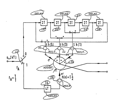
12. The filter of claim 11, wherein m = 0, wherein N = 11,
wherein the delay means has five delay members, and wherein the
third means comprises means for conveying the real component
sr(kT) weighted with h(5) to the input of the first delay member
of the chain, the real component weighted with -h(3) to the
input of the second delay member of the chain, the real component
weighted with h(1) to the input of the third delay member of the
chain, the real component weighted with -h(l) to the input of
the fourth delay member of the chain, the real component weight-
ed with h(3) to the input of the fifth delay member of the
chain, and the real component weighted with -h(5) to the output
of the fifth delay member of the chain.
13. The filter of claim 12, wherein the third means further
comprises means for conveying the imaginary component si(kT)
weighted with h(5) to the input of the first delay member of the
additional chain, the imaginary component weighted with -h(3) to
the input of the second delay member of the additional chain,
the imaginary component weighted with h(1) to the input of the
third delay member of the additional chain, the imaginary
component weighted with -h(l) to the input of the fourth delay
member of the additional chain, the imaginary component weighted
with h(3) to the input of the fifth delay member of the addition-
al chain, and the imaginary component weighted with -h(5) to the
- 23 - 27371-175
output of the fifth delay member of the additional chain.
14. The filter of claim 13, wherein h(0) = 1/2.
15. A nonrecursive half-band filter for filtering a complex-
valued input signal s1(kT)=s1r+js1i, where the input
signal has a sampling rate fA=1/T and where k is a running index,
the filter having a filter length N and having a pulse response
h(1), where N is an odd integer and l=-(N-1)/2 to (N-1)/2, said
filter comprising:
first means for demultiplexing the samples of the input sig-
nal to provide a plurality of demultiplexing signals, each de-
multiplexed signal having a sampling rate of fA/2; and
second means, receiving the demultiplexing signals, for
generating a filtered complex output signal ?(2kT) in accordance
with the following relationship, with the symbol * indicating
convolution and with h(1) representing a complex value
s(2kT) = s1(2kT)*h(1)
= s1r(2k)*hr(l) - s1i(2k)*hi(l) +
= j(s1r(2k)*hi(1) + S1i(2k)*hr(l)),
wherein the pulse response h(l) of the filter is modulated
onto a complex carrier with a frequency of +? of the sampling
rate fA to produce
?(1)=h(1).ej(?2.pi.1fA/(4fA)+?0)=j?1.ej?0.h(1)
and the zero phase ?0 of this frequency is a whole number
multiple m of .pi./2 (?0=m..pi./2, where m=0, 1, 2, 3, ...),
- 24 - 27371-175
wherein the plurality of demultiplexed signals includes first
and second demultiplexed signals,
wherein the first means includes means for forming the first
and second demultiplexed signals by allocating every second sample
of the real component of the input signal to the first demulti-
plexed signal and allocating the remaining samples of the real
component of the input signal to the second demultiplexed signal,
and
wherein the second means includes
a chain of (N-1)/2 delay members each having a delay of 2T,
the chain of delay members receiving the first demultiplexed sig-
nal,
means, receiving signals from the chain of delay members, for
forming difference signals, the means for forming difference sig-
nals including means for forming a first difference signal equal
to the output signal from the last delay member in the chain minus
the input signal to the first delay member of the chain, means for
forming a second difference signal equal to the output signal from
the penultimate delay member of the chain minus the input signal
to the second delay member of the chain, and means for forming a
third difference signal equal to the output signal from the third
delay member from the end of the chain minus the input signal to
the third delay member of the chain,
means for weighing the difference signals with values h(1) of
the pulse response,
means for summing the weighted difference signals to provide
- 25 - 27371-175
a contribution to one of the real and the imaginary components of
the filtered output signal,
a further delay member receiving the second demultiplexed
signal, the further delay member having a delay of T(N-3)/2, and
means for weighing the output signal of the further delay
member with the value h(0) to produce a contribution to the other
of the real and the imaginary components of the filtered output
signal.
16. The filter of claim 15, wherein the plurality of de-
multiplexed signals further includes third and fourth demulti-
plexed signals, wherein the first means further comprises means
for forming the third and fourth demultiplexed signals by alloca-
ting every second sample of the imaginary component of the input
signal to the third demultiplexed signal and allocating the re-
maining samples of the imaginary component of the input signal to
the fourth demultiplexed signal, and wherein the second means
further comprises
an additional chain of (N-1)/2 delay members each having a
delay of 2T, the additional chain of delay members receiving the
third demultiplexed signal;
means, receiving signals from the additional chain of delay
members, for forming additional difference signals, the means for
forming additional difference signals including means for forming
a first additional difference signal equal to the output signal
from the last delay member in the additional chain minus the
- 26 - 27371-175
input signal to the first delay member of the additional chain,
means for forming a second additional difference signal equal to
the output signal from the penultimate delay member of the addi-
tional chain minus the input signal to the second delay member of
the additional chain, and means for forming a third additional
difference signal equal to the output signal from the third delay
member from the end of the additional chain minus the input signal
to the third delay member of the additional chain;
means for weighing the additional difference signals with
values h(1) of the pulse response;
means for summing the weighted additional difference signals
to provide an additional contribution to one of the real and the
imaginary components of the filtered output signal;
an additional further delay member receiving the fourth de-
multiplexed signal, the additional further delay member having a
delay of T(N-3)/2; and
means for weighing the output signal of the additional fur-
ther delay member with the value h(0) to produce an additional
contribution to the other of the real and the imaginary components
of the filtered output signal.
17. The filter of claim 16, wherein N=11 and m=1, wherein
the first difference signal and the first additional difference
signal are weighted with -h(5), wherein the second difference
signal and the additional second difference signal are weighted
with h(3), wherein the third difference signal and the additional
third difference signal are weighted with -h(1), and wherein
h(0)=?.
- 27 - 27371-175
18. The filter of claim 16, wherein N=11 and m=3, wherein
the first difference signal and the first additional difference
signal are weighted with h(5), wherein the second difference sig-
nal and the additional second difference signal are weighted with
-h(3), wherein the third difference signal and the additional
third difference signal are weighted with h(1), and wherein
h(0)=?.
19. The filter of claim 16, wherein N=11 and m=0, wherein
the first difference signal and the first additional difference
signal are weighted with h(5), wherein the second difference sig-
nal and the additional second difference signal are weighted with
-h(3), wherein the third difference signal and the additional
third difference signal are weighted with h(1), and wherein
h(0)=?.
20. The filter of claim 16, wherein N=11 and m=2, wherein
the first difference signal and the first additional difference
signal are weighted with -h(5), wherein the second difference
signal and the additional second difference signal are weighted
with h(3), wherein the third difference signal and the additional
third difference signal are weighted with -h(1), and wherein
h(0)=?.
21. A nonrecursive half-band filter for filtering a complex-
valued input signal ?(2kT)=sr+jsi, where the input signal has
- 28 - 27371-175
a sampling rate fA'=?T and where k is a running index, the filter
having a filter length N and having a pulse response h(l), where N
is an odd integer and l=-(N-1)/2 to (N-1)/2, said filter
comprising:
first means, having first, second, third, and fourth input
ports and having first and second output ports, for multiplexing
signals received at the first and second input ports to provide a
signal at the first output port having a doubled sampling rate of
fA=2fA', and for multiplexing signals received at the third and
fourth input ports to provide a signal at the second output port
having a doubled sampling rate of fA=2fA'; and
second means, coupling the input signal to the input ports of
the first means, for generating at the output ports of the first
means a filtered complex signal ?2(kT) in accordance with the
following relationship, with the symbol * indicating convolution
and with h(1) representing a complex value
s2(kT) = s(kT)*h(1)
= sr(k)*hr(1) - si(k)*hi(1) +
j(sr(k)*hi(1) + si(k)*hr(1)); and
wherein the pulse response h(1) of the filter with respect to
the double sampling rate fA is modulated onto a complex carrier
with a frequency ?fA/4=fA'/2 to produce
?(1)=h(1).ej(?2.pi.lfA/(4fA)+?0)=j?l .ej?0.h(1)
and the zero phase 0 of this frequency is a whole number
multiple m of .pi./2 (?0=m-.pi./2, where m=0, 1, 2, 3, ...),
wherein the second means includes
- 29 - 27371-175
a chain of (.pi.-1)/2 delay members each having a delay of 2T;
an additional chain of (N-1)/2 delay members each having a
delay of 2T;
third means for conveying the real component sr(2kT)
weighted with predetermined values to the chain of delay members
to form a difference signal that is received at the first input
port of the first means, and for conveying the imaginary component
si(2kT) weighted with predetermined values to the additional
chain of delay members to form an additional differences signal
that is received at the fourth input port of the first means;
further delay means for delaying the imaginary component
si(2kT) weighted with h(0) of the pulse response to generate a
signal that is received at the second input port of the first
means, the further delay means having a delay of T(N-3)/2; and
additional further delay means for delaying the real compo-
nent sr(2kT) weighted with -h(0) to generate a signal that is
applied to the third input port of the first means.
22. The filter of claim 21 wherein in the third means the
real component sr(2kT) weighted with a value h(l) of the pulse
response is fed to the first delay member of the chain and is
subtracted from the output signal of the last delay member of the
chain, and the identically weighted imaginary component si(2kT)
is fed to the first delay member of the additional chain and sub-
tracting from the output of the last delay member of the addition-
al chain.
- 30 - 27371-175
23. The filter of claim 22, wherein the first means com-
prlses:
multiplexer means for generating the real component s2r(kT)
of the filtered signal by furnishing the difference signal as
every second sampling value of the real component and, offset in
time, by furnishing the output signal from the further delay means
as every second sampling value of the real component; and
additional multiplexer means for generating the imaginary
component s2i(kT) of the filtered signal by furnishing the addi-
tional difference signal as every second sampling value of the
imaginary component and, offset in time, by furnishing the output
signal from the additional further delay means as every second
sampling value of the imaginary component.
24. The filter of claim 23, wherein m=0, wherein N=11,
wherein the delay means has five delay members, and wherein the
third means comprises means for conveying the real component
si(kT) weighted with h(5) to the input of the first delay member
of the chain, the real component weighted with -h(3) to the input
of the second delay member of the chain, the real component
weighted with h(1) to the input of the third delay member of the
chain, the real component weighted with -h(1) to the input of the
fourth delay member of the chain, the real component weighted with
h(3) to the input of the fifth delay member of the chain, and the
real component weighted with -h(5) to the output of the fifth
delay member of the chain.
- 31 - 27371-175
25. The filter of claim 24 wherein the third means further
comprises means for conveying the imaginary component si(kT)
weighted with h(5) to the input of the first delay member of the
additional chain, the imaginary component weighted with -h(3) to
the input of the second delay member of the additional chain, the
imaginary component weighted with h(1) to the input of the third
delay member of the additional chain, the imaginary component
weighted with -h(1) to the input of the fourth delay member of the
additional chain, the imaginary component weighted with h(3) to
input of the fifth delay member of the additional chain, and the
imaginary component weighted with -h(5) to the output of the fifth
delay member of the additional chain.
26. The filter of claim 25, wherein h(0)=?.