Note: Descriptions are shown in the official language in which they were submitted.
- 1 3 1 1 857
~OW-COST HIGH-PERFORMANCE SEMICONDUCTOR C~IP PACXAGE
Field of the Invention
The present invention relates to the field of
electronic component bonding and packaging.
Back~round of the Invention
In the field of electronic component packaging
numerous problems exist. For example, the bonding of
conductive elements of a leadframe to a semiconductor chip
often results in c~ip passivation fractures during the
bonding process. These fractures may occur due to excessive
bonding force, misalignment occurring during the bonding
process, or inadequate standoff means to prevent the
conductive elements from being undesirably compresssd against
the semiconductor chip. Other fracture phenomena occur
during thermal cycling of components and result in poor
quality products which are either rejected or which perform
improperly. Further problems in the packaging field include
an inability to provide fine pitch geometries at various
levels of chip packaging to achieve the area utilization
demandQ of higher density devices. These all represent
particularly long-standing problems and constant challenges
in the packaging field, but ones which find solutions in the
present application in various ways.
Wasteful, inefficient, or unnecessary processing
steps in the production of semiconductor chips and other
electronic components accounts for substantial redundancy in
the packaging field. Moreover, as more complicated devices
require additional processing steps such devices become
increasingly susceptible to processing errors which may lead
to poor performance and low yields. In the field of
semiconductor chip production alone, the volume of chips
manufactured results in substantial numbers of improperly
packaged devices due to processing problems. Moreover, it
1 3 1`1 857
is quite common to experience low production yields in the
initial production phases of newly designed chips. By
streamlining and minimizing the steps required in a chip
production process, efficiencies combine to provide greater
overall yield percentages.
Yet a further problem identified in the prior art
of electronic component packaging includes devices which are
manufactured having inefficient utilization of chip surface
areas. Non-efficient structure in the packaging field is
tantamount to reducing the performance capabilities of the
electronic device. Rather, more ef~icient use of existing
space on an electronic component is the touchstone to
improved performance. Therefore, the more efficient use o~
the valuable chip surface area on electronic components
permits advanced capabilities, such as improved spacing and
pitch geometries. The present invention provides immediate
improvements affecting the production and operation of
electronic devices and assemblies which overcome these
problems identified above.
Various bonding techniques exist which permit
bonding of electronic components. These bonding techniques
include the use of relatively hard-bonding material, such as
gold, and soft-bonding material such as solder compositions.
Although the use of solder compositions is known in the art,
such compositions have generally been used as formations
which are placed on semiconductor chip devices during the
chip production process. Various compositions of solder have
been used, including tin-lead compositions. Commonly, soft
solder material is plated onto interface regions of
components as final processing steps prior to final component
testing. It has now been found valuable to apply soft
solder ~aterial, in the form of preformed solder bumps, to
131 1857
other structures in the packaging process. One example of
another structure is the conductive elements of a leadframe.
By placing preformed solder bumps on the conductive elements
of a leadframe, substantial efficiencies in the overall
production, packaging, and testing cycle occur. Alternately,
the present invention provides improved solder compositions
for strengthening the bonding capability of solder bumps
preformed onto semiconductor chips.
Therefore, the present application describes
improved packaging and bonding of electronic components to
achieve optimum signal fidelity, fine pitch geometries,
improved yield, greater reliability, and various
manufacturing efficiencies. The improvements comprise
several unique embodiments of tape leadframe technology,
solder bump transfer and bonding techniques, and preferred
bonding and fluxing material compositions.
Summary_~ the Invention
The present invention is a low-cost high-performance
semiconductor chip package enabling a direct chip to printed
circuit board connection. The package comprises a
semiconductor chip having a front surface and a back surface.
The front surface comprises pads for input and output of
signals to and from the chip. The package further comprises
a leadframe having power, ground, and signal conductive
elements having first and second end portions for
transmitting input and output signals to the pads. The
package also comprises a bonding system for selectively
connecting the first end portions of the conductive elements
to the pads and a protective system for providing sealed and
environmental protection around the semiconductor chip and
portions of the leadframe while permitting other portions of
1~1 1857
4 64159-1101
the leadframe to protrude from the protective means to provide
connection with other devices.
In accordance with the present invention there is
provided a low cost lead frame package, comprising: a) a
semiconductor chip having pads for input and output of signals
to and from the chip; b) a leadframe having power, ground, and
signal conductive elements for transmitting input and output
signals to the pads; c) bonding means for selectively
connecting the conductive elements to the pads; and d)
protective means for providing sealed environmental protection
around the semiconductor chip and portions of the leadframe
while permitting other portions of the leadframe to protrude
from the protective means to provide connection with other
devices, the protective means comprising: i) enclosure means
comprising inner chamber walls spaced away from the
semiconductor chip to permit independent thermal expansion
cycling of the semiconductor chip and the enclosure means; and
ii) stress relief means positioned between the chamber walls
and the semiconductor chip for relieving mechanlcal fatigue
caused by thermal stress to the chip, the leadframe, and the
protective means during thermal cycling.
1 3 t 1 857
Brief DescriPtion of the Drawinqs
Figure 1 is a perspective view of a representative
leadframe assembly.
Figure 2 is a perspective view of a representative
leadframe assembly with preformed solder bumps attached to
conductive elements.
Figure 3 is ~a perspective exploded view of a
leadframe assembly positioned over a solder bumped transfer
substrate.
Figure 4A illustrates a transfer substrate shown
with cavities and solder pellets within the cavities.
Figure 4B is a side sectional view along lines 4B-
4B in Figure 4A showing the solder pellets resting within the
transfer substrate cavities.
Figure 5 is a perspective exploded view of a
leadframe assembly with preformed solder bumps on conductive
elements positioned over corresponding bonding pads of a
semiconductor chip.
Figure 6 is a flow chart representation of prior art
semiconductor chip production cycle steps relating to the
deposition of solder bump material.
Figure 7A is a perspective view of a transfer
substrate with solder material deposited on it.
Figure 7B is a side elevation view of a solder
bumped transfer substrate analogous to that shown in Figure
7A following transfer of the solder bumps to a representative
semiconductor chip.
Figure 8A is a side elevation view of prior art non-
reflowed plated bumps positioned on a chip surface.
Figure 8B is a side elevation view of prior art
reflowed plated bumps illustrating non-uniform bump sizes.
- 6 _ l 3 1 1 8 5 7
Figure 8C is a side elevation view of preferred
high-yield high-density solder bumps prior to reflow.
Figure 8D is a side elevation view of the solder
bumps shown in Figure 8C after reflow.
SFigure 9 illustrates a side sectional view of a
stacked leadframe assembly and protective means.
Figure 10 illustrates a side sectional view of a
low-cost tab package and protective means.
Figure 11 is a flow diagram illustrating
representative prior art leadframe and chip assembly
proces es.
Figure 12 is a flow diagram illustrating a preferred
low-cost tab package leadframe and chip assembly process. ~
Figure 13A is a top plan view of an angled stress
relief means.
Figure 138 is a top plan view of an undulating
stress relief means.
Figure 13C is a side elevation view of an arched
stress relief means.
20Figure 14 is a side sectional view of a stacked tape
leadframe assembly.
Pigure lSA is a diagrammatic view of a
representative prior art leadframe and chip assembly
illu~trating a capacitor which is mounted externally of the
as~embly to a printed circuit board.
Figure 15B is a side sectional view of a filter
leadframe assembly partially within protective means and
mounted to a next level of packaging.
Figure 16 is a phase versus temperature diagram
showing a tin-lead composition.
Figure 17 is a side elevation view of a
representative belt furnace bonding mechanism.
131 1857
Figure 18 is a side sectional view of a leadframe
and chip holding device configured with a rigid insert to
achieve soft solder bump bonding uniformity.
Figure l9 is an enlarged side sectional view
generally corresponding to Figure 18 illustrating a leadframe
and chip holding device configured with a conformal insert
to achieve hard bump bonding uniformity.
~3~ 1857
-- 8 --
Detailed Descri~tion of the Preferred Embodiments
Detailed preferred embodiments of the present
invention are disclosed. It is to be understood, however,
that the disclosed embodiments are merely exemplary of the
S invention, which may be embodied in various forms.
~herefore, specific structural and functional details
disclosed are not to be interpreted as limiting, but rather
as a representative basis for teaching one skilled in the art
to variously employ the present invention in virtually any
appropriately detailed system or structure. It will be
understood that in some circumstances relative material
thicknesses and relative component sizes may be shown
exaggerated to facilitate an understanding of the invention~
Inventions described in the present application
relate to improvements in packaging and bonding electronic
components to achieve finer pitch geometries, improved yield,
improved reliability, and manufacturing efficiencies. The
improvements include several unique preferred features
including tape leadframe constructions, solder bump transfer
bonding techniques, and preferred bonding and fluxing
material compositions.
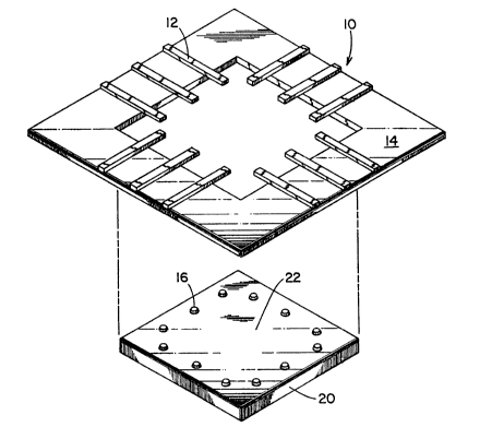
Referring to Figure 1, an exemplary leadframe 10 is
illustrated. It is appreciated that leadframes are variously
constructed and shaped; however, the basic function of
leadframes is to provide conductive elements for use in
interconnecting the leadframe with at least one other
electronic device. Leadframe 10 comprises conductive
elements 12 for transmitting input and output signals to
bonding locations on an electronic device. Leadframes 10 may
comprise a tape leadframe having dielectric material 14 for
separating the conductive elements. Dielectric material 14
may also be constructed and arranged to provide cushioning
131 1857
_ 9 _
during bonding as well as stress relief during operation
and/or temperature cycling of the device.
As the complexity of electronic devices increases,
the demands of properly packaging such high performance
and/or multi-lead devices become more challenging. Indeed,
current semiconductor chips may require several hundreds of
bonds per chip in the packaging process. Specifically,
certain chip capacities are now between about 600 to 800
bonds per chip. It is expected within the field of packaging
technology that near-term bonding requirements will exceed
2000 bonds per chip. However, as the number of bonding
operations per chip increases, the stress on each chip also
increases as each bond is formed; other potential sources of
chip failure or rejection also increase as the number of
bonding operations increase.
One method of reducing the number of bonding
operations per chip is to align a leadframe, such as
leadframe 10, with appropriate bonding locations on a
semiconductor chip and then exert a single bonding force to
the leadframe to effect multiple bonds simultaneously. When
using such a technique, commonly called ~'gang-bonding", the
problems of using hard bonding materials are best
exemplified. When using a hard bonding material with gang
bonding, greater force is needed to effec~ a compression bond
than if the bonding material were more soft. Accordingly,
compression bonding of hard bonding material frequently
results in undesired chip passiva~ion cracking and over-
compression of conductive elements of the leadframe.
Although the use of tape leadframes provides certain
advantages relating to self-alignment and vertical standoff
of the conductive elements of the leadframe with respect to
bonding interface regions on chips, the use of soft solder
131 1857
-- 10 --
material is also of great value. Heretofore, soft bonding
material, such as solder bonding material or soft solder, has
been confined to placement on active electronic device
interface regions rather than onto a leadframe. However, the
placement of preformed solder material onto leadframe
conductive elements relieves the active electronic
components, such as chips, from potential adverse effects
related with such processes. Perhaps even more
significantly, by preforming solder bumps to leadframe
conductive elements rather than to devices such as chips, the
devices themselves can be tested for acceptability before
they are integrated into a leadframe assembly or even a chip
carrier. Therefore, it is desirable to place preformed
solder bumps 16 on leadframe conductive elements to achieve
an overall improvement in device yield and reliability.
Further, by placing preformed solder bumps on leadframe means
10 the bonding material may be inspected independent of the
chip production process and independent of the process
wherein leadframes are mated with other devices.
Accordingly, as illustrated in Figure 2, a leadframe
assembly is provided having conductive elements 12 preformed
with solder bumps 16 for use in interconnecting the leadframe
with an electronic device. Preferably, leadframe 10
comprises at least one of power, ground, and signal
conductive elements for transmitting input and output signals
to bonding locations on an electronic device. Also, solder
bumps 16 are preformed onto conductive elements 12 in a
pattern which will permit bondinq with desired bonding
locations on an electronic device. Preferably, preformed
solder bumps 16 comprise a tin and lead composition.
A method of manufacturing a leadframe assembly
having preformed solder bumps, which may also be referred to
131 1857
11
as a bond-when-ready bumped leadframe, is provided. This
method preferably comprises the steps of positioning
leadframe 10 for receipt of preformed solder bumps 16 onto
conductive elements 12, and then attaching the solder bumps
at desired locations on the conductive elements. Preferably,
the solder bumped conductive elements may then be selectively
bonded with bonding locations on an electronic device. As
illustrated in Figure 3, the step of preforming solder bumps
16 comprises providing a non-solderable transfer substrate
having a transfer surface 22 for receipt of solder
material in the form of solder bumps or deposits 16. The
solder material is deposited onto transfer sùrface 22 to form
solder deposits in a predetermined pattern. Conductive
elements 12 of leadframe 10 are then aligned and mated with
patterned solder bumps 16. Finally, the conductive elements
and patterned solder bumps are heated to the point of reflow
to permit the solder deposits to transfer into wetted contact
with the leadframe 10 conductive elements 12.
Solder material may be deposited onto transfer
substrate 20 in several different ways. The deposition step
may be accomplished by positioning a conventional shadow mas~
on transfer surface 22 and than evaporating solder material
through apertures in a shadow mask to form preformed solder
deposits 16 on transfer surface 22. Alternately, solder
material may be plated onto transfer surface 22 using
conventional plating techniques. Yet another method of
preforming solder deposits 16 onto a transfer substrate 20
includes providing a non-solderable transfer substrate, as
shown in figure 4A, having a plurality of cavities 32
configured for positioning preformed solder material. Then,
preformed solder pellets 34 are deposited onto the transfer
surface for nesting in cavities 32 in a predetermined
- 12 - 131~
pattern, as illustrated in Figures 4A and 4B. Preferably,
transfer substrate 20 comprises a reusable material for
multiple transfers of solder material.
A method of constructing a leadframe assembly is
also provided in which the conductive elements are preformed
with solder bumps for bond-when-ready packaging of a
semiconductor chip. .This method comprises providing a
leadframe 10 preferably comprising at least one of power,
ground, and signal conductive elements 12, and preforming
solder bumps 16 onto conductive elements 12 of leadframe 10
to provide means for selectively bonding the conductive
elements to semiconductor chip bonding pads. The various
methods of depositing preformed solder bump material onto
leadframe 10 as described above pertain to this embodiment
as well. Although other methods of depositin~ preformed
solder bump material onto transfer substrate 20 and leadframe
10 are available, thos~ identified above are preferable.
This solder bump transfer technology permits transfer of
preformed solder bump material to active die and wafers, in
addition to leadframes. Certain other advantages accrue by
use of this transfer substrate technology, and will be later
discussed in greater detail.
Specific applications of preformed solder bumped
leadframes include advantageous connecting of bumpless
semiconductor chips and other devices to preformed solder
bumped leadframes. Indeed, the overall concept of bumping
leadframes and in particular soft solder bumping of the
leadframes is intended to take the bumping process out of the
chip production cycle. In other words, the chip experiences
no bumping process until bonded to the leadframe. This is
important for several reasons, not the least of which is time
and efficiency. This process prevents exposing the chip to
131 1857
- 13 -
potential yield problems and plating techniques such as
voltage spiking, plating current generation, or plating
corrosive action from plating solutions. Also, it is not
uncommon for extremely low yields to result from the first
6 months of a new production process for chips. Indeed,
effective yields may only then curve up to maximums of
between 60% to 80% per.production batch over several years.
Therefore it i5 quite important to minimize yield problems
wherever feasible. By utilization of a pre-tested reliable
inventory of unbumped chips, increased batch yields may be
realized. Stated another way, by taking the bumping process
out of the chip production cycle, only 100~ yield bumped
leadframes and 100% yield chips will be used when bonding.
This permits separating the chip fabrication process from
the bumping process without adverse impact on any of the
components. This also permits parallel processing and
production which in the past was combined as a single, less
efficient, serialized event. This method of manufacture
enhances cost reductions and permits bond-when-ready
assembly.
Another advantage of applying solder bumps to
leadframe conductive elements relates to the prior art
problem of solder fatigue due to neutral point distancing.
This problem arises when chips include bumps which are
positioned on surfaces of a rigid substrate which expand due
to thermal cycling or operation at a rate different than the
chip. This often results in separation of the bump from the
chip and degraded chip operation. In contrast, by placing
the solder bumps on leadframe conductive elements which are
substantially independent from these thermal stresses noted
above, the bumps remain attached. This advantage provides
improved reliability.
5 /
- 14 -
Therefore, this invention provides a low-cost high-
yield semiconductor chip and leadframe assembly kit. As
illustrated in Figure 5, this kit preferably comprises a
semiconductor chip 42, leadframe 10, and bonding means
comprisinq solder bumps 16 preformed to leadframe 10.
Preferably semiconductor chip 42 comprises wetable, non-
reflowable interface regions 46, also commonly referred to
as pads, for input and output of signals to and from the
chip. Leadframe 10 preferably comprisas a leadframe having
power, ground, and signal conductive elements 12 for
transferring signals to and from chip 42 interface regions
46. This invention also encompasses a reduced process high-
yield semiconductor chip and leadframe assembly k~t
comprising a semiconductor chip 42 comprising bumpless
interface pads 46 for input and output of signals to and from
chip 42, and leadframe 10 comprising a leadframe including
solder bumped conductive elements 12 arranged for reflow
bonding with chip pads 46.
A method of manufacturing a low-cost high-yield
leadframe assembly, as illustrated in Figure 5, includes
providing a semiconductor chip comprising wetable, non-
reflowable interface pads for input and output of signals to
and from the chip; aligning a leadframe comprising preformed
solder bumped conductive elements with the interface pads or
regions and reflowing the preformed solder bumps for
conductively interconnecting the leadframe conductive
elements with the chip interface pads. Similarly, a method
of manufacturing a reduced process high-yield leadframe
assembly comprises positioning a semiconductor chip
comprising bumpless interface pads for input and output of
signals to and from the chip; aligning leadframe conductive
elements with the interface pads, the leadfr~me comprising
1 3 1 1 857
- 15 -
means for reflow bonding the conductive elements to the chip
pads; and reflow bonding the leadframe to the chip.
Preferably, the method of reflow bonding a reduced process
high-yield leadframe assembly comprises reflowing solder
bumps which were previously preformed onto the conductive
elements.
Pigure 6 is a schematic representation of exemplary
prior art chip production process steps. As shown in Figure
6, the process of plating solderable bumps to semiconductor
chips or wafers typically comprises numerous steps integral
to the chip production cycle. These steps normally comprise
providing an integrated circuit wafer and first depositing
a field metalization. Next, photo-resist techniques are
employed and the sites for metalized bumps are defined by
etching holes in the photo-resist. A layer of interface
metal is then deposited into the etched holes. Then,
metalization to form the bumps is plated onto the interface
metal. The metalization may be a tin-lead composition. The
bump metalization is then reflowed and the steps of etching
the field metal follow. Finally, the metalization is again
reflowed to provide smooth and readily bondable metalized
bumps. The tab may then be bonded to the metalized bumps on
the integrated circuit chip or wafer. The current low-cost
tab package leadframe invention eliminates substantially all
of the process steps illustrated in Figure 6, and therefore
reduces chip production cycle time as well dS reducing risk
of damage to the chip. This is particularly relevant to
semiconductor chips which are either expensive to manuf~cture
or which require long production cycles. Indeed, substantial
commercial advantage may be realized by reducing production
cycles and providing greater ability for parallel production
techniques.
- 16 - 1 3 1 t 85 7
The current pre-bumped leadframe invention provides
means for achieving the above objectives by providing pre-
bumped leadframes for bond-when-ready attachment to bare,
e.g. non-bumped, chips or wafers. This is greatly
advantageous over the prior art in that it permits
independent chip inspection as well as independent bump
inspection prior to th~ bonding process so that a very high-
yield, if not lO0~, of operational devices may be achieved
quite readily. Note that this process eliminates the
wasteful steps involved in bumping semiconductor chips prior
to testing the chip, as is commonly done and as shown in
Figure 6. Due to these advantages, this invention may also
be described as a maximum yield pre-bumped invention.
In the event that pre-bumped chips are desired, e.g.
maintaining the wasteful production steps of the prior art,
then substantial improvements in bonding reliability may
still be achieved according to tha present single phase
solder composition invention, described in greater detail
later in this application.
It is appreciated that the use of vapor deposition
and plating as means for providing reflowable solder material
for bonding electronic devices is generally well known in the
art. However, such processes have neither addressed nor
solved many problems related to prior art processes. In
particular, prior art techniques of vapor depositing solder
material onto active die or wafers include placing a shadow
mask comprising numerous apertures onto the surface of an
active die or wafer. The assembly is then placed in a
chamber where the solder material is evaporated and deposited
onto the wetable portions of the wafer that are exposed
through the apertures of the shadow mask. Frequently,
however, difficulties arise with respect to the shadow mask
13~ 1857
- 17 _
scratching portions of the active die or wafer. Such
scratching may lead to considerable reliability and yield
problems affecting active components. Also, as the
requirement for higher density devices increases, the masks
S must include more apertures. Substantial problems related
to aperture density and mask planarity result. For example,
insufficient separation between apertures provides only
partial bump laydown on the active wafers.
Yet another problem occurs when excess solder
material passes through certain apertures causing electrical
bypasses on the active wafer or die. This phenomenon may
also be caused by certain masking processes which result in
the effect known as "haloing." This "haloing" leaves
undesirable residue on active die which is avoided through
use of the present invention. Furthermore, the evaporation
process used in the prior art requires exposure of the active
wafer or die to the temperature and pressure variations
associated with conventional vapor deposition techniques.
Indeed, the heat generated during the evaporation process
causes certain masks to adhere to and damage the active
device. Elimination of this damage to the active wafer or
die is desirable. Also, if an active wafer or die receives
only a partial bump or metalization laydown, the active
component must either be discarded or further processed in
order to achieve a proper pattern of solderable material.
Once again, neither of those options are desirable or
efficient.
One solution to these problems of vapor deposition
processes includes manufacturing a high-yield solder bumped
semiconductor wafer using new methods. One such method,
illustrated in Figure 7A, includes providing a non-solderable
transfer substrate 20 having a transfer surface 22 for
- 18 - 1311857
receipt of solder material. Solder material is then
deposited onto transfer surface 22 to form solder bumps 16
' in a predetermined pattern, as shown in ~igures 7A and 7B.
The deposition of the solder material onto transfer surface
22 may be accomplished by either plating, vapor deposition,
or pellet placement in cavities as earlier referred to and
explained in this applLcation. Next, as shown in Figure 7B,
the method includes aligning solderable conductive elements
70 of a semiconductor wafer 72 with the patterned solder
bumps 16 on transfer surface 22, and then heating and
reflowing the patterned solder bumps into wetted contact with
wafer 72 conductive elements 70. Thus, this process
eliminates the problems described above which reduce th~
reliability of prior art active devices exposed to process
steps now rendered unnecessary by the invention just
described.
Thus, the present solder bump transfer invention
permits production of high-yield solder bumped semiconductor
wafers 72 without risk of scratching by a shadow mask, and
without any transfer of residual solder material such as that
which forms halos on prior art active die. Additionally, the
above preferred method of manufacturing a high-yield solder
bumped semiconductor wafer avoids the difficulties associated
with the conventional plating process of solder bumping
active wafers and die. The previously mentioned problems of
voltage spiking, current generation, and acidic corrosion are
overcome by utilizing intermediate transfer substrate 20 as
described above. Also, exposure of the active device to the
prolonged cycle time associated with the plating process is
avoided.
Yet another problem relating to the prior art
plating of active die involves the characteristic mushrooming
131 1857
-- 19 --
shape of solder bumps formed on active die using the plating
process, as shown in Figure 8A. ~his results in waste of
space due to the normally expanded diameter at the top
portion of such solder bumps. Accordingly, the prior art
process of plating active die is density limited and of
little value when attempting to manufacture fine pitch
geometry devices. This phenomenon, wherein a solder bump
includes a mushroom shaped top portion over a narrower base,
results in such conventional plating being only good to pitch
densities of about 8 mil. In contrast, use of the transfer
method described above according to the present invention
permits bump spacing of at least as small as about 1 to 2 mil
and, therefore, achieves the objectives of tighter pitch
geometry construction, as represented in Figure 8C. Indeed,
by comparing the bump spacing using prior art plating
techniques before and after reflow, shown in Figures 8A and
8B, and comparing the finer pitch bump spacing according to
the present transfer method invention, shown in Figures 8C
and 8D, the advantage is quite clear. Also, as shown in
Figure 8A and 8~, the prior art plating process promotes
greater potential for uneven bump sizes due to the increased
possibility that the pre-reflow mushroom shaped deposits will
be in contact.
Although later detailed discussion will relate to
the preferred compositions of solder bondin~ material, the
above method of manufacturing a high-yield solder bumped
semiconductor wafer preferably further comprises use of
solder material comprising less than 3% by weight tin.
In the field of electronic packaging, performance
characteristics of individual electronic components may be
improved in various ways. One such technique is to optimize
the use of existing space on an electronic device as
131 1857
- 20 -
illustrated in Figures 9 and 14. The embodiment of the
present invention shown in Figures 9 and 14 represents
improved means for space utilization on a component by use
of a stacked tape leadframe assembly 54. More particularly,
stacked tape leadframe assembly 54 provides means for
arranging multilayer conductive leads access to more area of
an electronic compone~t as well as on various vertically
spaced lines or layers. Stacked tape leadframe assembly 54
is designed for use with integrated circuit chips and
comprises multiple leadframes 54 arranged in stacked
relation. Each leadframe 54 preferably comprises at least
one conductive element 62. Solder bump means comprising
solder bumps 66 are provided for electrically and
mechanically connecting selected conductive elements 62 of
leadframes 54. As is further illustrated in Figure 14,
preferred stacked leadframes 54 comprise non-wetable surfaces
comprising dielectric material 70 for maintaining separation
between adjacent leadframes 54 and for dielectrically
separating multiple conductive elements within a leadframe.
Also, preferred stacked tape leadframe assembly 54 and solder
bumps 66 are constructed and arranged to connect conductive
elements 62 with integrated circuit chip 72.
Figure 14 shows one embodiment of stac~ed tape
le~dframe assembly 54 comprising a first upper leadframe
labelled U including a conductive element 62u, a second lower
leadframe labelled L comprisinq a conductive element 621, and
a third middle leadframe labelled M comprising a conductive
element forming a signal line 62m positioned in stacked
relation between the first and second leadframes to form a
constant impedance stripline, or constant impedance
microstrip configuration. The dimensions of leadframes 54
and their conductive elements define the electrical
- 21 _ ~ 3 1 ~ 85 7
parameters of any circuit formed. Indeed, con~uctive
elements 62 may also comprise ground conductors or ground
planes. Alternately, certain conductive elements 62 may
comprise power conductors, and such power conductors may
further be configured as power planes. As previously noted,
conductive elements 62 may also comprise signal lines.
Referring no~ to Figure 9, a stacked leadframe
assembly 54 is shown. Stacked leadframe assembly 54
preferably comprises multiple leadframes 58 arranged in
stacked relation with each leadframe comprising linear
conductive elements 62. Also, solder bump means is provided
comprising stacked solder bumps 66 for electrically and
mechanically connecting conductive elements 62. Figure 9
particularly shows a stacked leadframe assembly 54 with
protective means 76. Preferred protective means 76 is
located around portions of stacked leadframe assembly 54
while permitting other portions of the stacked leadframes to
protrude from protective means 76 to provide connection with
other devices.
This stacked tape leadframe assembly invention thus
incorporates a plurality of discrete leadframes connected
mechanically and electrically through the use of stacked
leadframes. Accordingly, stacked tape leadframe assembly 54
solves problems associated with signal management of high
speed integrated circuits, such as characteristic impedance
control, inductance, capacitance, resistance and cross-talk
noise. Stacked tape leadframe assembly 54 may be configured
as a controlled impedance structure by regulating the height
of solder bumps 66 or by configuring other physical
characteristics of leadframes 54. Thus, stacked tape
leadframe assembly 54 provides innovative cost reductions
over conventional multilayer ceramic printed circuit boards
- 22 _ 1 3 1 1 8 5 7
and packages while also providing significant perf~rmance
advantages.
~ eferring now to Figure 10, a side sectional view
of a low-cost leadframe package 84 is illustrated. Low-cost
leadframe package 84 provides substantial savings during the
production process as well as substantial reliability
improvements during operation. As shown in Figure 10, low-
cost leadframe package 84 preferably comprises a leadframe
86, a semiconductor chip 88, bonding means comprising a
plurality of originally preformed solder bumps 16, and
protective means 76 for providing sealed and environmental
protection around semiconductor chip 88 and portions of
leadframe 86 while permitting other portions of leadframe 86
to protrude from protective means 90 to pro~ide connection
with other devices. Preferably, low-cost leadframe package
semiconductor chip 88 comprises a chip front surface ~2 and
a chip back surface 93, with chip front surface 92 comprising
pads 96 for input and output of signals to and from chip 88.
Leadframe 86 preferably comprises at least one of power,
ground, and signal conductive elements 100 having first end
portions 101 and second end portions 102 for transmitting
input and output signals to pads 96. Preferably, protective
means 76 comprises enclosure means preferably comprising
first and second enclosure members 112, 113 respectively,
which form a chamber around semiconductor chip 88. Inner
surfaces of enclosure members 112, 113 comprise chamber walls
114 which preferably are spaced away from semiconductor chip
88 to permit independent thermal expansion cycling of chip
88 and enclosure members 112, 113. Protective means 76
preferably also comprises barrier sealing means 116 for
coating and protecting semiconductor chip 88 from
environmental contamination, and package sealing means 117
- 23 - 131 1857
for sealing the interface between enclosure members ~2, 113
or between protective means 76 and a next level of packaging.
Protective means 76 may also further comprise stress
relief means 120, shown in Figures 10, 13A, 13B, and 13C,
positioned between chamber walls 114 and semiconductor chip
88 for relieving mechanical fatigue caused by thermal stress
to chip 88, leadframe. 86, and protective means 76 during
thermal cycling. Stress relief means 120 preferably
comprises a stress relief expansion portion 122 of conductive
elements 100 configured for maintaining conductivity of
signals passing from leadframe 86 to and from chip 88
independent of thermal cycling induced stresses.
Figure 13A illustrates a top view of stress relief means 12
configured as an angular stress relief means 120a.
Similarly, Figure 13B illustrates a top view of an undulating
stress relief means 120b constructed and arranged to relieve
mechanical fatigue caused by thermal stress to chip 88,
leadframe 86, and protective means 76 during thermal cycling.
Figure 13C is a side elevation view of stress relief means
120 configured as a flexible arched stress relief means 120c.
Therefore, the preferred low-cost leadframe package
invention encapsulates the semiconductor with an open cavity
126. Further, the portion of leadframe 86 which is within
cavity 126 preferably comprises stress relief means 120 to
minimize fatigue caused by thermal stresses. Accordingly,
the invention preferably includes encapsulated stress relief
expansion means 120 for permitting thermal expansion induced
movement of the components without losing conductivity or
without causing device failure. Further, this is important
in that it allows choices of different component materials
which might otherwise experience mutually unacceptable
thermal expansion differences. Another way of stating this
- 24 - ~31 ~857
feature is that this low-cost package maintains condu~tivity
for signals passing to and from the leadframe and the chip
' independent of thermal cycling induced stresses.
At least one of enclosure members 112, 113 of low-
cost leadframe package 84 may comprise a next level of
packaging. Also, second end portions 102 of conductive
elements 100 may comprise means for connecting package 84 to
a printed circuit board 130 without intermediate packaging.
This demonstrates yet another advantage of the present low-
cost package invention which includes cooling featuresrelating to how chip 88 is connected to the package.
Specifically, semiconductor chip 88 front surface 92 is
configured with chip pads 96 and back surface 93 is
configured for bonding to a portion of protective means 90.
This configuration takes advantage of the thermal resistance
feature in back-side mounting by placing more area of the
chip in contact with a heat-sink during operation than if the
heat to be dissipated had only the solder bond and air to
provide heat sinking. Stiffening means may also be provided
in the package t~ facilitate mounting on a printed circuit
board or other level of packaging. Low-cost leadframe
package 84 barrier sealing means 116 preferably comprises
polyimide material while the bonding means preferably
co~prise~ solder bump material.
Low-cost leadframe package 84 may also comprise a
high-d~nsity low-cost leadframe package configured for direct
connection with a printed circuit board or other level of
packaging. The high-density low-cost leadframe package would
preferably comprise a semiconductor chip 88 having bonding
pads 96 comprising fine pitch bonding pads with a pattern
repetition of substantially less than 0.02 inch (.51 mm).
Similarly, leadframe 86 may comprise fine pitch conductive
t31 18~7
elements, and the bonding means may comprise m~ns for
connecting the fine pitch conductive elements to the fine
pitch pads. This high-density low-cost leadframe package
embodiment preferably comprises pads 96, located on
semiconductor chip 88, and leadframe conductive elements lO0,
which are spaced at a pitch of between about 0.003 inch (.076
mm) and 0.008 inch (.2Q3 mm). Preferably, those portions of
conductive elements 100 extending outside protective means
90 are spaced at a pitch of between about 0.004 inch (.102
mm) and about 0.010 inch (.254 mm).
Referring again to Figure 10, a method of
constructing low-cost leadframe package 84 is disclosed.
Preferably, this method of construction comprises the steps
of providing semiconductor chip 88 having pads 96 for input
lS and output of signals to and from the chip, and positioning
a leadframe 86 for connection with chip 88. Preferably
leadframe 86 comprises at least one of power, ground~ and
signal conductive elements lO0 with first end portions 101
and second end portions 102 for transmitting input and output
signals to pads 96. A chip and leadframe package is then
formed by bonding conductive elements 100 to chip pads 96
using preformed solder bumps 16. Then, protective means 76
is placed to provide sealed and environmental protection
around semiconductor chip 88 and portions of leadframe 86
while permitting other portions of leadframe 86 to protrude
from protective means 76 to provide connection with other
devices. A preferred method of construction includes
protective means 76 comprising a first enclosure member 112
and a second enclosure member 113 placed around semiconductor
chip 88 to form a chamber. Preferably, the enclosure members
each comprise inner surfaces comprising chamber walls 114
spaced away from semiconductor chip 88 to permit independent
- 26 - 1311857
thermal expansion cycling of chip 88 and enclosure~members
112, 113. Further, a preferred method of assembling the
above device includes connecting conductive element second
end portions 102 with a printed circuit board 130 without
intermediate packaging.
It is appreciated that the method described above
may include use of a leadframe comprising a tape leadframe
having a plurality of conductive elements separated and
carried by tape means such as a dielectric material. In
addition to providing protective means 76,- stress relief
means 120 may be provided. More particularly, the method of
construction of low-cost leadrame package 84 preferably
further comprises the step of positioning stress relief mean~
120 between chamber walls 114 and semiconductor chip 88 for
relieving mechanical fatigue caused by thermal stress to chip
88, leadframe 86, and protective means 76 during thermal
cycling.
Within the field of packaging technology,
substantial costs are expended in bonding die or active
devices to leadframes. This expense is driven by the ever
increasing number of bonds per die which are required.
Therefore, as the capabilities of semiconductor chips
increase, so also does the number of bonds per die. Various
developments have been suggested in the art to reduce the
time and energy required to bond die to leadframes but a
repre~entative pattern of process steps has emerged as an
industry practice. Figure 11 schematically represents the
prior art process of tab assembly. As illustrated in Figure
11, a first leadframe must be attached to the die. Then, the
die is excised from the first leadframe and epoxy bonded to
the package. The first leadframe must then be at~ached to
the package and a lid must then be welded thereon. However,
13t 1857
- 27 -
further steps are required. These steps include bom~ing the
second leadframe to the package in order to provide a
conductive path from the die through the package to external
devices. Only then is the assembled package ready for
functional test. It is not uncommon in the prior art to have
a requirement of in excess of 1000 bonds per tab assembly.
The present low-cost tab package invention identifies and
eliminates numerous prior art tab assembly steps. Indeed,
as illustrated in Fiqure 12, the low-cost tab package
invention requires fewer process steps and a greatly reduced
number of bonds per assembled die. Particularly, as shown
in Figure 12, the low-cost tab package invention requires
attaching a leadframe to a die. Then the chip i~ epo~y
bonded to a package. Next, a lid is sealed on the package
and the package is then ready for functional test. As
illustrated in Figure 10, the innovation of providing a
protective means around a continuous leadframe eliminates the
requirement in the prior art for hundreds of bonds on most
high performance chips. A simple measure can be made of the
enormous impact this invention has on large scale chip
production processes. For example, the savings per chip in
numbers of bonds eliminated as compared with identical
interconnect requirements in the prior art readily exceeds
50~, and the reliability is greatly increased. This great
reduction of bond requirements per chip has enabled the
applicant to manufacture these devices achieving production
efficiencies heretofore unknown.
Figure l5B illustrates another leadframe
configuration designed for improved signal performance. As
shown, filter leadframe assembly 162 is provided for
improving the signal-to-noise ratio in high performance
packaging. Preferred filter leadframe assembly 162 comprises
1 3 1 1 857
- 28 -
a leadframe 164 having conductive elements 166 for providing
at least one of power, ground, and signal conductive paths
to and from electronic components such as a semiconductor
chip. Capacitor means for providing electrical decoupling
to the leadframe assembly is provided. Preferably, capacitor
means comprises at least one decoupling capacitor 169
attached between power and ground conductive elements of
leadframe 164.
Signal fidelity in typical leadframe devices is
degraded by electrical noise which may otherwise be
eliminated or minimized by use of decoupling capacitors 169
arranged according to the present filter leadframe invention.
The closer to a semiconductor chip's power and ground
connections that a particular decoupling capacitor is placed,
the more effective the noise reduction capability of that
capacitor becomes. Conventional decoupling capacitors are
typically mounted on printed circuit boards and packages as
shown in Figure 15A. However, by mounting decoupling
capacitors 169 directly onto leadframe 164, as shown in
Figure 15B, the capacitors are now located virtually as close
as possible to the respective power and ground connections
in order to maximize their decoupling effect. Various means
of attaching decoupling capacitors 169 to leadframe power and
ground conductive elements 166 are available, such as use of
solder paste, solder preforms, or conductive epoxy. Filter
leadframe assembly 162 preferably comprises a tape leadframe
having dielectric material 173 for separating conductive
elements 166. Conductive elements 166 are preferably
comprised of copper material.
As shown in Figure 15B, filter leadframe assembly
162 may also include integral component means comprising a
semiconductor chip 178 having interface regions 180 for input
- 29 - 1311857
and output of signals to and from the chip. Semico~ductor
chip 178 is preferably connected to leadframe 164 so that at
least one decoupling capacitor 169 is positioned above chip
interface regions 180 to provide signal decoupling while
minimizing the separation between chip 1~8 interface regions
and capacitor 169.
Filter leadframe assembly 162 may further comprise
protective means 76. Protective means 76 is constructed and
arranged to provide sealed and environmental protection
around semiconductor chip 178 and portions of tape leadframe
164 while permitting other portions of tape leadframe 164 to
protrude from protective means 185 to provide connection with
other devices. Figure 15B further illustrates filter
leadframe assembly 162 having leadframe second end portions
188 extending from protective means 185 to provide a
connection with a printed circuit board 190 without any
intermediate packaging. The open regions may be provided in
filter leadframe assembly 162 to provide flexure and prevent
fracture or cracking of the assembly.
The present solder composition invention, to be
discussed next, relates to a system of packaging and bonding
electronic components to achieve manufacturing efficiencies,
improved performance, and greater reliability. Significant
improvements in electronic package reliability have been
achiovQd according to the teachings of this invention by use
of soft solder bump compositions. Althouqh various
compositions may be utilized, it is preferable to use a
composition which maintains a single solid phase
metallurgical state throughout a wide range of thermal
environments. For example, it is not uncommon for electronic
components to be exposed to diverse operating environments
ranging from very high temperatures to well below roOm
~ 30 ~ ~J t 1 8 5 7
temperature. Many conventional bonding compositions
experience phase changes between solid and liquid during such
temperature migrations which lead to metal fatique. This
clearly répresents an undesirable characteristic, causing
substantial reliability problems for systems and components
using such bonding materials.
The present solder composition invention discloses
a preferred tin-lead solder composition ~hich maintains a
single phase solid at ~ubstantially wider temperature ranges
than is presently experienced by solder bonding material used
in the field of electronic bonding compositions. More
specifically, use cf a composition co~.prising less than 3%
by weight of tin and more than 97~ by weight of lead results
in substantially higher reliability bonds. For example~
testing of 1% by weight tin solder bumps reveals reliability
figures which exceed those of higher tin content bu~ps, such
as 3% to 6% by weight tin, by a factor of thrce timee.
Referring now to Figure 16, a simplified tin-lead
phase diagram is provided. The tin-lead composition
illustrated will be totally liquid and in complete solution
at the temperatures above line A B C. Line A B C is ~hus
referred to as the liquidus of this system. Therefore, all
of the region marked I is complately li~uid. Reyions II and
III in the diagram marked Beta (P) and Alpha (~),
respectively, are areas of solid solution. ~hen an a'loy of
a given composition and a given temperature falls within the
regions of and ~, it will have a single phase. Lines A D
and C F, which form the upper limits of these regions, are
called the solidus as is line D F. Any mater-al underneath
solidus A, D, F, C, will be a complete solid. The material
in area IV consists of a coMbination of p and ~ in various
ratios. The curvature of lines F G and D ~ indicates that
131 1857
- 31 -
the amount of solute (primary element) in the solid solution
of regions II and III diminishes with cooling and that area
IV consists of a double phase where ~ and ~ coexist in
various configurations. Regions V and VI as shown in the
S diagram lie between the solidus and the liquidus of the
system and therefore consist of ~ plus liquid and ~ plus
liquid, respectively. These regions are usually labelled the
pasty range. Most known solder compositions for electronic
bonding reside in this pasty range. However, as solid
crystals of ~ or o are disbursed in a liguid solution of tin
and lead and as the temperature is lowered, the liquid can
no longer dissolve the large quantity of the second phase,
and more crystals of ~ and ~ are formed unti~ a eutectic
temperature is reached or the balance of the material freezes
totally in a mixture of 3 and ~.
As shown in Figure 16, line Q represents an alloy
having 90% by weight lead and 10~ by weight tin. As the
alloy migrates from high temperature liquid solution to
cooler temperatures, it passes through various metallurgical
phases. Upon initial cooling it passes first into the pasty
range where the alloy starts forming crystals of 3 in region
VI. Upon further cooling the alloy totally freezes in the
form of a solid ~ phase in region III. Yet as the alloy
cror~-~ line F G to a cooler temperature, the solid solution
can no longer hold all of the tin and a formation of the
phase results in a two phase region shown by the ~ and
coexistence in region IV.
As Figure 16 further illustrates, only in the case
of compositions similar to that represented by line R, which
is a 98~ by weight lead and 2% by weight tin composition,
would a single phase of ~ exist at normal room temperatures.
Indeed, such low tin content compositions provide the widest
- 32 - t31 1857
range of a single phase solid solder composition.= As a
result, soft solder bonding material made from very low tin
content alloys experience no metallurgical phase changes
during wide ranges of operating temperature, thus increasing
the bonding material reliability and resistance to thermal
induced fatigue.
Accordingly,_it is preferable to utilize a soft
solder bonding material for providing conductive electronic
component high-strength bonding which maintains a single
phase solid state between such wide temperature ranges of at
least approximately -65C to approximately 200C. Preferred
soft solder bonding material comprises a tin and lead
composition. Thus, a composition is desirable whic~
comprises tin and lead wherein the percent by weight of tin
is substantially equal to or less than the value at which the
composition changes from the single phase solid ~ state to
the two phase solid ~ plus ~ state at substantially 0C.
This tin lead composition solder bonding material may further
comprise a solder bump configured for preformed placement and
subsequent reflow bonding between electronic components.
As illustrated in Figure 16, preferred solder
bonding material, which may be in the form of a solder bump,
comprises less than 3% by weight of tin and more than 97% by
weight of lead in order to optimize the thermal cycling range
of s~ability. More particularly, preferred solder bump
material for use in interconnecting electronic components
comprises between about .5% to about 2% by weight of tin, and
between about 98% to about 99.5% by weight of lead.
Components manufactured within this preferred tin content
range were thermal cycled from -65C to lS0C beyond 1000
cycles without failures. In contrast, previous tests using
131 1857
- 33 -
approximately 3% to 6% tin content solder bonding ~terial
experienced failures at 200 or less cycles.
It is appreciated that at least some applications
of preferred soft solder bonding material according to the
present solder composition invention may be suitable for use
in environments outlined within U.S. Department of Defense
Military Standard 883. Accordingly, a solder bonding
material, which may be in a preformed bump configuration, is
provided for conductive electronic component high-strength
bonding which exceeds by an order of magnitude the minimum
number of 100 thermal cycles required by U.S. Department of
Defense Military Standard 883 method 1010 over a temperature
of -65C to 150C. This solder bonding material preferably
comprises an effective amount less than 3~ by weight of tin,
and more than 97~ by weight of lead. More specifically, such
solder bonding material preferably comprises a composition
of between about .5% to about 2% by weight of tin, and
between about 98% to about 99.5% by weight of lead.
Another way of stating the present solder
composition invention is to provide a solder bonding material
for conductive electronic component high-strength bonding
which exceeds by an order of magnitude the minimum number of
100 thermal cycles required by U.S. Department of Defense
Military Standard 883 method 1010 over a temperature range
of -65C to +150C and which comprises a composition of tin
and lead wherein the percent by weight of tin is
substantially equal ts or less than the value at which the
composition changes from the single phase solid ~ state to
the two phase solid ~ plus ~ state at substantially 0C.
Similarly, the present invention discloses a solder bump
material for use in interconnecting electronic components
comprising a composition for maintaining a single phase solid
~ 34 ~ 1311857
state over the temperature range of U.S. Department ~f
~ Defense Military Standard B83 method 1010 of -65C to 150C
thermal cycling requirements.
As previously mentioned, the use of this solder
composition invention may include placing the solder
composition on semiconductor chips to provide high-
reliability bonding in a manner not previously known or
appreciated in the field of electronic packaging technology.
The present solder composition invention further
comprises a leadframe assembly having conductive elements
preformed with high-strength solder bumps for use in
interconnecting the leadframe with an electronic device.
This leadframe assembly preferably comprises leadframe means
compri~ing at least one of power, ground, and signal
conductive elements for transmitting input and output signals
to bonding locations on an electronic device. The leadframe
also preferably comprises solder bumps preformed on the
conductive elements for selective bonding with bonding
locations on the electronic device. The solder bumps
preferably comprise a composition for maintaining a single
solid phase over the temperature ranges of 0C to 150C.
Alternately, the solder bumps of this leadframe assembly may
compri~e about .5~ to about 2% by weight of tin, and about
98~ to about 99.5% by weight of lead. ~oreover, the solder
bump~ of the leadframe assembly may comprise both a
composition for maintaining a single solid phase over the
temperature range of 0C to 150C as well as about .5% to
about 2% by weight of tin and about 98% to about 99.5~ by
weight of lead. A leadframe assembly having any of the above
solder bump composition characteristics may further comprise
a tape leadframe having dielectric material for separating
the conductive elements.
_ 35 _ 1311857
This solder composition invention further discloses
a method of manufacturing a bond-when-ready bumped leadframe
comprising the steps of providing a leadframe comprising at
least one of power, ground, and signal conductive elements;
and preforming solder bumps onto the conductive elements to
provide means for selectively bonding the conductive elements
to bonding locations o an electronic device, and the solder
bumps being preformed having a composition for maintaining
a single solid phase over the temperature ranqe of 0C to
150C. Alternately, the solder bump composition of the
solder bumps to be preformed as part of the above method of
manufacturing a bond-when-ready bumped leadframe may comprise
a composition of about .5% to about 2% by weight of tin, and
about 98% to about 99.5% by weight of lead. Indeed, a
lS preferred method of manufacturing a bond-when-ready bumped
leadframe may comprise solder bumps with a composition for
both maintaining a single solid phase over the temperature
range of 0C to 150C and comprising about .5% to about 2%
by weight of tin and about 98% to about 99.5% by weight of
lead.
A low-cost high-strength leadframe and semiconductor
chip assembly is also provided according to the present
solder composition invention. A preferred low-cost high-
strength leadframe and semiconductor chip assembly comprises
a aemi~onductor chip comprising bonding locations for input
and output of signals to and from the chip. The assembly
further comprises leadframe means comprising at least one of
power, ground, and signal conductive elements for
transmitting input and output signals to ~he bonding
locations on the semiconductor chip. Also, this low-cost
high-strength leadframe and semiconductor chip assembly
comprises solder bump means comprising solder bumps reflowed
- 36 - 1311857
between corresponding leadframe conductive eleme~ts and
bonding locations on the semiconductor chip. The solder
bumps preferably have a composition for maintaining a single
solid phase over the temperature range of 0C to 150C.
Alternately, the solder bumps may have a composition
comprising about .5% to about 2% by weight of tin, and about
98% to about 99.5% by weight of lead. However, yet another
low-cost high-strength leadframe and semiconductor chip
assembly according to this solder composition invention
comprises solder bump means comprising solder bumps having
a composition for maintaining a single solid phase over the
temperature range of 0C to 150C, and that composition
comprises about .5~ to about 2% by weight of tin and about
98% to about g9.5% by weight of lead. Similarly, a method
of manufacturing a low-cost high-strenqth leadframe and
semiconductor chip assembly is provided. Preferred steps for
this assembly method comprise providing a semiconductor chip
comprising bonding locations for input and output of signals
to and from the chip; providing leadframe means comprising
at least one of power, ground, and signal conductive elements
for transmitting input and output signals to the bondinq
locations on the semiconductor chip; providing solder bump
mean3 comprising solder bumps positioned between
corresponding leadframe conductive elements and bonding
locations of the semiconductor chip, the solder bumps having
a composition for maintaining a single solid state phase over
a temperature range of 0C to 150C; and reflowing the solder
bumps to join the corresponding leadframe conductive elements
with the bonding locations on the semiconductor chip. The
composition of the solder bumps in the above preferred method
may comprise about .5% to about 2% by weight of tin, and
about 98% to about 99.5% by weight of lead rather than being
131 1857
- 37 -
defined by having a characteristic property of mai~taining
a single solid phase over a temperature range of 0C to 150C
only. However, yet another preferred method of manufacturing
a low-cost high-strength leadframe and semiconductor chip
S assembly includes solder bumps having a composition
comprising about .5% to about 2% by weight of tin and about
98% to about 99.5% by weight of lead, and that
composition maintains a single solid phase over a temperature
range of 0C to 150C.
This solder composition invention further comprises
a method of manufacturing a low-cost high-strength leadframe
and semiconductor chip assembly following the steps of
providing a semiconductor chip comprising bonding locations
for input and output of signals to and from the chip; bonding
leadframe means comprising at least one of power, ground, and
signal conductive elements for transmitting input and output
signals to the bonding locations on the semiconductor chip;
providing solder bumps preformed to the semiconductor chip
bonding locations, the solder bumps having a composition for
maintaining a single solid phase over the temperature range
of 0C to 150C; aligning the solder bumps preformed on the
semiconductor chip bonding pads with corresponding leadframe
conductive elements; and reflowing the solder bumps to join
th~ corresponding leadframe conductive elements with the
bonding locations on the semiconductor chip. This method of
manufactùring a low-cost high-strength leadframe and
semiconductor chip assembly may alternately comprise solder
bumps having a composition comprising about .5% to about 2%
by weight of tin, and about 98% to about 99.53 by weight of
lead.
Yet another preferred embodiment of this solder
composition invention comprises a low-cost high-yield high-
131 1857
- 38 -
strength semiconductor chip and leadframe assembiy kit
comprising a semiconductor chip comprising bonding locations
for input and output of signals to and from the chip; a
leadframe having at least one of power, ground, and signal
conductive elements for transferring signals to and from the
chip bonding location; and bonding means comprising solder
bumps preformed to t~.e leadframe conductive elements for
selective bonding with bonding locations on the semiconductor
chip, the solder bumps comprising a composition for
maintaining a single solid phase over a temperature range of
0C to 150C. The solder bumps may further comprise a
composition comprising about .5% to about 2~ by weight of
tin, and about 98~ to about 98.5% by weight of lead.
Alternately, this assembly ~it may comprise bonding means
comprising solder bumps preformed to the leadframe conductive
elements for selective bonding with bonding locations on the
semiconductor chip. The solder bumps may comprise about .5~
to about 2~ by weight of tin, and about 98% to about 98.5%
by weight of lead. Further advances in the field of
packaging and bonding of electronic components include the
following improved furnace bonding structure and method.
The basic furnace bond technique of electronic
component bonding is well known. A device to be bonded is
placed in a furnace for heating and low-force bonding of
conductive elements. A frequent problem arises, however, in
unequal compression forces being applied to various
conductive elements being bonded. Often, this unbalanced
bonding force results in overcompression of certain
conductive elements and insufficient compression being
applied to other conductive elements. In each case, the
reliability of the overall package is degraded. Accordingly,
the present invention provides means for controlled
_ 39 _ t 3 1 1 8 5 7
compression furnace bonding of conductive elemen~s of a
leadframe to a semiconductor chip without experiencing the
compression problems in the prior art. Specifically, a
bonding system 208, shown in Figure 17, is provided
comprising holding means having a holding memb~r with a chip
support surface for supporting a semiconductor chip,
positioning means for precisely positioning conductive
elements of a leadframe with bonding locations on the
semiconductor chip, and furnace heating means comprising a
furnace for heating and reflow bonding the conductive
elements to the chip bonding locations.
As illustrated in Figure 17, a representative
furnace bonding cycle comprises furnace means which is
preferably a belt furnace 210 configured for heating the
conductive elements and the semiconductor chip which are both
- retained in a holding member 212. The belt furnace 210
preferably comprises a belt member 215 which transports
holding member 212 through the belt furnace 210. Preferred
belt furnace 210 comprises means for creating a neutral or
reducing atmosphere surrounding locations on the chip where
the conductive elements are to be bonded. This neutral or
reducing atmosphere thereby permits fluxless bonding of the
materials.
As illustrated in Figure 18, means for positioning
the semiconductor chip in holding member 212 is provided.
Vacuum means is configured in chamber 220 for creating a
vacuum to temporally hold the semiconductor chip 223 and to
facilitate fine alignment of chip 223 with conductive
elements 225 of a leadframe 226. Chamber 220 also minimizes
the exposure of chip 223 to heat retaining portions of
holding member 212. The positioning means further comprises
a clamp spring assembly represented by force arrows labellad
- 40 - 131 1857
J for securely clamping the positioned chip 223 and le-adframe
226 prior to heating the chip in furnace 210. Preferably,
bonding device 208 positioning means further comprises
alignment pegs 230 constructed and arranged for engaging and
aligning leadframe 226. Also, surfaces 232 defining
alignment holes 233 are located in holding member 212 as
shown. Alignment holes 233 are preferably constructed and
arranged for slidable receipt of alignment pegs 230. As
illustrated in Figure 18, the interaction of alignment pegs
230 and alignment holes 233 provides coarse alignment to
conductive elements 225 in relation to chip 223 bonding
locations.
Holding member 212 illustrated in Figure i7
comprises means for maintaining lead-to-bump alignment as
lS well as for ensuring the required contact between solder
bumps 235 and conductive elements 225. The contact between
solder bumps 235 and conductive elements 225 is achieved
through use of either a rigid insert or a conformal insert.
The rigid insert 240 is constructed and arranged for use with
soft solder bump applications. Rigid insert 240 is
preferably placed on top of leadframe conductive elements 225
which are arranged vertically above chip 223. Thus, rigid
insert 240 exerts a gravity generated compression force on
the leadframe and ensures that conductive elements 225 are
all sufficiently contacting appropriate chip bonding
locations. The controlled compression effect of placing
rigid insert 230 on conductive elements 225 promotes uniform
bonding of each conductive element 225 with semiconductor
chip 223 independent of any initial non-planarity of
conductive elements 225 and any difference in bump heights
of solder bumps 235 located on chip 223. Preferred insert
material includes a quartz material due to its excellent
- 41 - 13tl857
thermal isolation characteristics. When using bondin~ device
208 according to the present invention, it is also desirable
to provide standoff means 242 for maintaining the vertical
height of conductive elements 225 in relation to chip 223.
Alternately, a hard bonding material may be utilized
to maintain the conductive element height above the chip
surface 244. However~ use of hard materials may lead to
cracking or other damage to chip 223 when compression bonding
force is applied. Therefore, as illustrated in Figure l9,
conformal insert 248 may be utilized. Conformal insert 248
is constructed and arranged to function similarly to rigid
insert 240 with the exception of permitting nominal insert
compression to accommodate different heights among bumps made
of hard material located on chip 223. This characteristic
eliminates one source of manufacturing process component
damage and thus enhances the reliability of components made
with the present invention. Bonding device 208 may be
utilized with conductive elements having preformed reflowable
solder bumps attached. Preformed reflowable solder bumps may
also be configured as earlier described and shown on chip
223. Also, rigid insert 240 and conformal insert 248 are
readily interchangeable to facilitate efficiency and reduce
tooling requirements.
Material savings and component cleanliness is
enhanced when the present furnace bonding invention is
utilized in a neutral or reducing atmosphere surrounding
solder bumps 235 during the bonding process. When the
process is accomplished within a nitrogen atmosphere,
fluxless bonding may be achieved.
Accordingly, a method is provided for controlled
compression furnace bonding of a semiconductor chip to
conductive elements of a leadframe. This method comprises
~ - 42 - 1311857
the steps of placing a semiconductor chip 223, as s~own in
Figure 18, comprising a plurality of bonding locations in a
holding member 212 comprising a chip support surface 222;
providing preformed bonding material for connecting
conductive elements 225 of a leadframe 226 with the chip
bonding locations; aligning the leadframe conductive elements
with the bonding locat ons on the semiconductor chip; moving
the leadframe conductive elements toward the chip bonding
locations so that the bonding material contacts the
conductive elements and the chip bonding locations; heating
the bonding material to a point of reflow; and cooling the
bonding material to complete the bonding process. This
method may further comprise the step of creating a neutra~
or reducing atmosphere surrounding the bonding material
during the bonding process. Also, the step of positioning
the semiconductor chip preferably comprises placing the chip
on a chip support surface above a chamber extending into the
holding member; creating a vacuum for temporally holding the
chip while precisely aligning the chip with the leadframe
conductive elements; and locking the chip in alignment with
the leadframe conductive elements prior to heating the
assembly. The positioning of preformed bonding material may
comprise positioning preformed solder bumps on the leadframe
conductive elements or on the semiconductor chip bonding
locstion3.
In the event that fluxless furnace bonding is not
utilized, then a fluxing agent according to the present
invention can provide for improving the bonding process by
yet other means. For instance, the present fluxing agent is
particularly cost effective because its preferred
constituents are inexpensive, readily available, and easily
mixed. Furthermore, expenses related to cleaning bonded
131 1857
- 43 -
surfaces, after these surfaces are bonded with prior art
fluxing agents, can be substantially reduced because the
present fluxing agent minimizes or substantially eliminates
the charring which generally occurs when the prior art
fluxing agents are used. The use of a fluxing agent or flux
is generally not necessary when using gold bonding material.
However, when using solder bonds in normal atmospheres, it
is necessary to use flux to promote oxide-free surfaces for
~oining at the bond site. Activated fluxes such as those
with ammonium chloride, zinc chloride, hydrogen chloride, or
other well known activating agents are generally quite acidic
and can be toxic. The residue that is often left behind
after use of activated fluxes can corrode components an~
cause other difficulties. In contrast, use of a preferred
lS fluxing agent, containing oil and rosin, leaves a
substantially inert residue which, even when left on the
component surface, will not cause the problems associated
with the activated fluxing agents noted above. Prior
solutions to the problems of charring and corrosive flux
residue have included use of alcohol constituents combined
with flux or flux constituents. The alcohol tends to
evaporate, however, thereby reducing its effectiveness. When
isopropyl alcohol is used in a fluxing agent including water
whita rosin, the flux often dries and chars during the
tabbing process and is difficult, if not virtually impossible
to clean. The charred flux can prove to be a source of ionic
contamination, or an aesthetic problem. The present fluxing
agent preferably utilizes a combination of rosin and oil to
solve the ongoing problem of charring of bonding areas.
The preferred fluxing agent preferably includes
low-cost, readily available, and normally non-hazardous
materials. The preferred fluxing agent is easily mixed and
1 31 1 857
- 44 -
dispensed, and is easily removed from the bondi~g site.
Because the present fluxing agent preferably includes an oil
or combination of oils which have ignition temperatures which
are preferably greater than the temperatures required to bond
solder to a surface, the charred residue, which often results
from the burning of prior art fluxing agents, is
substantially minimized.or eliminated. The preferred fluxing
agent comprises between about 5-9S, preferably 10-90, more
preferably 20-80, even more preferably 30-70~ by weight of
oil and between about S-95, preferably 10-90, more preferably
20-80, even more preferably 30-70% by weight of rosin.
Another fluxing agent according to this invention consists
essentially of about S-gS% by weight of oil and about 5-95~
by weight of rosin. The addition of oil to the rosin adjusts
the viscosity of the flux, thereby making it easier to handle
and dispense. However, the addition of the oil has not been
found to decrease the effectiveness of the rosin in
minimizing the formation of oxides during soldering. Indeed,
it is believed that the addition of the oil may enhance the
effectiveness of the rosin, particularly for use with
structures having fine geometry spacing. Furthermore, the
stability of this combination of constituents is important
in that during the temperature increases of the bonding
process, the respective percentages of oil and rosin in the
flux mixture remain substantially the same.
The preferred oil will preferably have an ignition
temperature of at least about 375C. By selecting an oil
having a relatively high burning temperature, the tendency
of flux to char during bonding is minimized. Accordingly,
an oil or a combination of oils may be utilized providing
that the oil or combination of oils has an ignition
temperature of preferably at least about 375C. Preferred
131 1857
- 45 -
oils may be selected from the group consisting of v~getable
oils, fish oils, animal oils, mineral oils, and the like or
combinations thereof. The preferred oil or combination of
oils preferably has an ignition temperature of at least about
390, more preferably about 400, even more preferably about
415 and still more preferably about 425C. It is most
preferable that the oLl which is selected for use from the
above group have an ignition temperature of at least about
430C. When using a vegetable oil, it is preferable to
select the oil from the group consisting of peanut oil,
sunflower oil, rapeseed oil, soybean oil, castor oil, jojoba
oil, corn oil, and the like or combinations thereof. It will
be appreciated that other well known oils exhibiting high
ignition temperatures can also be utilized. Most preferably,
the vegetable oil is peanut oil and has an ignition
temperature of at least about 430C.
It is generally believed that as the percent by
weight of rosin in the preferred fluxing agent approaches
50%, the advantages of the preferred fluxing agent are
realized more fully. For example, as composition of rosin
approaches 50% the fluxing agent is readily flowable for
dispensing and use. Furthermore, it is believed that as the
percent by weight of rosin is increased, the anti-charring
characteristic of the preferred fluxing agent becomes more
apparent during bonding, and the amount of charring which
occurs is minimized. Consequently, the preferred fluxing
agent preferably comprises at least about 30, more preferably
about 40, still more preferably about 50% by weight of rosin.
Furthermore, the ratio of the percent by weight of rosin to
percent by weight of oil is preferably at least about 0.1,
more preferably about 0.5, even more preferably 0.75, still
131 1857
- 46 -
more preferably 0.9, even more preferably 0.9~, most
preferably about 1.
The choice of rosin for use in the preferred fluxing
agent is preferably a substantially inert, non-activated
rosin. The preferred rosin preferably comprises water white
rosin which is commercially available from numerous sources;
however, other rosins exhibiting non-activated
characteristics can also be utilized. The preferred oil and
rosin combination provides a non-corrosive and non-toxic
fluxing agent which is preferable for use with electronic
components and which is generally not harmful to personnel
in contact with it. Also, when the intended use does not
demand a non-activated rosin for electronic safety or other
reasons, the present fluxing agent may include an activated
rosin which is compatible with the preferred oil composition.
Because the preferred embodiments of the present
fluxing agent substantially eliminate charring and the
production of charred residue during soldering operations,
cleaning of the soldering surface is much easier. For
example, the use of especially harsh or toxic cleaning agents
is unnecessary. Such surfaces are easily cleaned using
relatively mild cleaning agents such as warm xylenes, dry
acetone, or the like.
A method for bonding a conductive element with
solder is also provided. This method preferably comprises
- the steps of placing solder and a fluxing agent on a surface
of the element to be bonded~ the fluxing agent preferably
having between about 5-95% by weight of oil and between about
5-95% by weight of rosin. The next step comprises heating the
surface, the solder and/or the flux to a temperature of
between about 250-400C, wherein charring of the fluxing
agent is minimized. It is believed that bonding
1 3 1 ~ ~57
- 47 -
substantially occurs at temperatures of between abo~t 250-
400, preferably 300-400C, and that if charring can be
minimized at those temperatures by the inclusion of an oil
or oils having relatively high ignition temperatures, then
S the charring effect seen with prior art fluxes can be
substantially minimized or eliminated.
Example 1
An equal amount by weight of a commercially
available peanut oil having an ignition temperature of 443C
and water white rosin distributed under the trade name ~Alpha
5002" is mixed together and agitated for approximately 2
minutes at a moderate speed in a glass mixer. The resulting
fluxing agent is smooth, viscous, and readily dispensable.
When the resulting fluxing agent is applied to a leadframe
surface and solder is heated to a reflow temperature of 325C
proximate to this surface substantially no charring occurs.
It is to be appreciated that while certain
embodiments of the present invention have been illustrated
and described, the invention is not to be limited to the
specific forms or arrangements of parts described and shown
above, since others skilled in the art may devise other
embodiments still within the limits of the claims.