Note: Descriptions are shown in the official language in which they were submitted.
``` ` 131~6~
DEVICES HAVING SHALLOW JUNCTIONS
This invention relates to the fabrication of integrated circuits (ICs) and in
particular to the fabrication of ICs relying on complementary metal oxide on silicon (CMOS)
configurations.
A detailed discussion of the background to this invention will be given
hereinbelow.
Shallow junctions are obtainable while relative latch-up immunity, and
acceptable leakage current are maintained through the use of a specific device configuration.
This configuration depends on p-channel souroe and/or drain junction dopant region(s) in the
N-tub 1) that are shallower than 1200 A, 2) that have a dopant concentration that yields a
reverse leakage current with an activation energy lower than the bandgap energy of silicon and
3) that have a dopant conoentration profile that is highest at the silicide interfaoe.
In one embodiment to produce this configuration 1) the silicide precursor
region is converted to the silicide before implantation, 2) the silicide and not the underlying
silicon is implanted with a dose of p-type dopant such as boron dopant, e.g., B or BF2, typically
in the range 1 x 10l5 to 1 x 10l6 cm-2 and 3) the implanted region is heated to a temperature in
the range 700C to 925C for a time period typically in the range 30 to 180 minutes for
conventional furnaoe heating or temperatures in the range 800C to 1000C for the shorter
periods required by rapid thermal annealing. By controlling p-channel source and/or drain
2 0 junction dopant, the inventive devioe has improved latch-up holding voltage, e.g., 4 volts, a
leakage current as low as 10-l5 amps/~m2, and an Rc that is a small percentage of the device
channel resistance. A relatively small junction contribution to the device resistance occurs
because the dopant concentration of only the p-channel devioe is constrained to obtain the
desired latch-up and leakage current characteristic. Since the p-channel device, as compared
2 5 to the n-channel device, has a relatively high resistance, the larger p-channel junction
resistance remains negligible.
In accordance with one aspect of the invention there is provided an article
comprising a substrate, said substrate comprising silicon and having an N-tub and a P-tub with
corresponding p-channe; MOS and n-channel MOS devioes, said p-channel MOS and
n-channel MOS devices including a junction for electrical communication with said channel,
char.lcterized in that said junction ol` said p-channel MOS devioe comprises a metal silicide
f~
131~
region overlying a p-type junction dopant region wherein the average thickness of said dopant
region is 1200 ~ or thinner, the dopant concentration in said dopant region is highest at said
silicide/dopant region interface, and the activation energy of the reverse leakage current for
said junction between said dopant region and said N-tub is less than 1.12 eV.
The present invention will be described in detail hereinbelow, with the aid of
the accompanying drawings, in which:
FIGs. 1 and 2 are illustrative of configuration involved in the inventive devices;
and
FIGs. 3 through 7 are illustrative of attainable properties.
Prior to discussing the present invention, a brief discussion of the background
for this invention will be given.
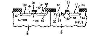
A widely employed IC configuration involves CMOS technology. In this
configuration and N- and P-tub are formed as shown at 1~ and 19 of FIG. 1. (The N and P
tubs have respective electrons and holes as the majority carrier). The gate semiconductor
material 20 and 21 is generally n type. The device channel regions 40 and 42 are generally the
same carrier types as their respective tubs (although not necessarily), but when inverted during
operation conduct through a majority carrier opposite to that of the associated tub. Material
having the opposite majority carrier from their underlying tubs are used as source and drain
regions 30 and 31. The depth 50 in FIG. 1, of the source and drain junctions are strongly
2 0 influenced by the device design rule, i.e., the siæ of the smallest feature critical to the device
operation such as the width 60 of the gate in FIG. 1. (The junction depth is defined as the
average depth measured in a direction normal to the plane of the silicon substrate
(immediately before the first step in source and drain formation) and from this plane to a
point where the material changes from n to p type.) As design rules become stricter, e.g.,
2 5 ~ates become narrower, the depth of the junctions must be correspondingly shallower to
maintain acceptable device performance. For example, the junction depth should-be no
greater than about 0.25 llm for a design rule of 0.75 ~m or smaller.
Additionally, t`or stricler design the decrease in device dimensions prod`uces astrong tendency for the two parasitic bipolar transistors shown in FIG. 2 to produce a
catastrophic current flow (denominated latch-up) in response to a transient excursion in
operaling voltage. Thus~ the regions forming these parasitic transis~ors should be
advan~ageously tailored to lessen this tendency without unacceptabl! degrading other electrical
proper~ies such as leakage current. However, suggested approaches for reducing latch-up
tendencies ~enerally add process complexi~ies (e.g., insulating regions for isolation),
131~
unacoeptably increase leakage current or increase spacing between devioes. Additionally,
solely addressing latch-up properties is not enough. To achieve relatively low junction
resistanoe while employing a relatively shallow souroe and drain, a metal silicide, 64, e.g.,
tungsten silicide or titanium silicide, overlying junction dopant regions, 62 and 63, is desirable.
5 This region serves as a low resistanoe current shunt between the shallow junction dopant
region and its respective electrical contact.
A variety of attempts have been made to produce relatively shallow souroe and
drain silicided junctions while obtaining a degree of latch-up immunity and maintaining an
acoeptable leakage current, e.g., a current less than 10-~2 amps/llm2 for typical CMOS
l0 applications. In one method described by Lau et al. (IEEE Transactions on Electronic
Devioes, ED-33 (9), 1308 (1986)), a precursor to the metal silicide is formed in the junction
region. For example, when titanium silicide is desired, titanium is deposited onto the silicon
substrate in the junction region. The precursor region is implanted with a suitable dopant;
arsenic and/or phosphorus for the n-channel devices in the P-tub and born entities for p-
15 channel devioes in the N-tub. The wafer is then heated to form the metal silicide and to drive
a portion of the dopant from the silicide into the underlying region to form the junction
dopant regions 62 and 63. Although reportedly this junction has relatively good latch-up
immunity, the depth of the resulting junction is significantly greater than desirable for strict
design rules.
Another suggested approach for shallow junction fabrication is described by
Kobayashi et al. in a paper entitled "Comparison of TiSi2 and WSi2 Silicide Shallow Junctions
for Sub-micron CMOSs," Abstract of papers, 1986 Symposium on VLSI technology, San
Diego, CA. In this method, the precursor region is produced and heated to form the silicide.
This silicide is then implanted and heated to induce partial diffusion of the implanted dopant
2 5 from the silicide region into the underlying silicon to form the junction dopant region.
Junction depths of .28 and .23 ,um were obtained for tungsten and titanium silicide,
respectively.
The tungsten silicide junction obtained by Kobayashi is, thus, too deep for strict
design rules. The titanium silicide region is relatively shallow. However, the dopant profile in
30 the junction (as shown in FIG. 1 of the Kobayashi abstract) increases for at least 700 A from
the silicide/silicon interface into the underlying silicon. If all the implanted dopant had been
con~`ined initially in the silicide region, the dopant concentration ~ould monotonically decrease
into the silicon from the silicide/silicon interface. Thererore, the profile actually obtained
indicates that a significant level of dopant had been implanted below the silicide. Indeed,
3 5 Kobayashi discusses the desirability of implanting additional arsenic into the underlying silicon
- 13~6~
to increase dopant concentration, and presumably, to lower the junction resistance. This
implantation procedure, however, is undesirable because the resulting implant damage must be
removed by high temperature annealing to ensure acceptable leakage currents. As a
consequence of the annealing, the junctions are significantly deepened beyond the region
desirable for 0.75 llm or small design rules.
As discussed, the invention involves a device having a shallow junction, a
junction shallower than 2500 A, that is relatively latch-up immune, that has an acceptable
leakage current, and that has a relatively low contribution to device resistance from the
junction region. (In the context of this invention improved immunity to latch-up is a 10
percent increase in holding voltage relative to a device where dopant is implanted into a non-
silicide region, e.g., silicon or a silicide precursor. However, it is even more desirable to have
improvements of S0 percent or greater). The desired electrical properties are obtained by
adjusting the depth and dopant concentration of the junction dopant region. Thisconcentration should be sufficiently small so that the activation energy of reverse leakage
current across the junction is less than the band gap energy of silicon, i.e., 1.12 electron volts.
(Recombination-generation centers formed by defects or by dopants, such as gold, lower
activation energy but substantially increase leakage current. Although their presence is not
precluded, it is not desirable because of the effect on leakage current. The activation energy
of reverse current across the junction is determined by measuring reverse bias junction leakage
current vs. temperature as described by C. Barrett et al., The Principles of En ineerin
Materials, Prentice-Hall, Englewood Cliffs, New Jersey, 1973, pp. 148 and 149).
Most significantly the adjustment of dopant concentration and depth to yield an
activation energy less than 1.12 electron volts is required only for the p-channel devices. In
these devices, the channel resistance is generally two to four times greater than that of the n-
2 5 channel devices. As a result, the contribution to device resistance from the lower dopant
concentration is not particularly significant relative to the higher channel resistance of the p-
channel devices. In this manner the operating characteristics of the device are not
unacceptably altered while relative latch-up immunily and acceptable leakage current are
obtained.
3 o A suitable expedien~ for obtaining the inventive devices involves the formation
of a silicide junction region followcd by implantation of dopant into this region and diffusion
of a portion of this dopant into thc underlying silicon to form thc junction dopant region. A
process involving silicide lormation lollowed by implantation and ~liffusion is described in U.S.
Patent No. 4,914,500 which issued on April 3, 1990 to R. Liu, et al.
~ 3 ~ ~ Q~
Basically this procedure, in one embodiment, involves depositing a
metal onto a silicon substrate in the source and drain juncdon regions. Typically,
to maintain junctions shallower than 0.25 ~m the deposited material should have a
thickness generally in the range .01 to .05 ~lm. Thicknesses less than .01 ~m
S yield inadequate silicide formation while thicknesses greater than .05 ~m lead to
excessive junction depth.
Formation of the silicide is accomplished by heating the substrate to a
temperature generally in the range 400C to 900-C. The precise temperature
employed depends on the particular material used. For exarnple, a suitable
10 temperature protocol for cobalt is generally a first treatment in the range 400-C to
SOO-C to convert the precursor to the monosilicide followed by a treatment in the
range 700-C to 800-C to convert to the disilicide, while temperatures in the range
600-C to 900-C are typically employed for dtanium. The duradon of the heating
should be sufficiently short so that the established dopant profiles throughout the
15 device are not substandally altered due to diffusion. Typical dmes in the range
15 minutes to 2 hours for conventional heating and 1 second to 2 hours for rapidthermal anneals are employed. A control sample is easily employed to determine
a desirable temperature and treatment dme for a desired device configuradon and
silicide composition.
The silicide is then implanted with a dopant entity suitable for
forming the dopant juncdon region. Typically for an n-type juncdon region an
arsenic and/or phosphorus implantation is used while for a p-type juncdon regiona boron endty, e.g., B or BF2 implantadon is employed. The acceleradon voltage
of the implantadon apparatus should be controlled so that the peak concentratdon25 of the implanted ions lies within the silicide, and preferably lies a distance from
the silicide/silicon interface into the silicide of at least 0.10, most preferably 1/3,
of the average silicide thickness. (The silicide thickness at any point is measured
in a directdon normal to the substrate surface).
The implanted dopant concentration limits the level of dopant that is
30 introduced after diffusion into the dopant juncdon region. Typically, implanted
doses in the range 1 x 10l5 to 1 x 1016cm~2 are employed. The diffusion
temperature and treatment dme is controlled to induce a dopant concentradon in
the juncdon dopant region that yields an activation energy of the reverse leakage
current of less than 1.12 electron volts. The precise combinadon of time and
35 temperature to yield this result varies with the material silicide, the thickness of
the silicide, the implanted dopant, and the concentration of the dopant. Generally,
1 3 ~
diffusion temperatures in the range 750 to 925C are employed in conjunction with diffusion
times in the range 15 to 180 minutes. A control sample is easily employed to determine the
precise conditions required for a given combination of device parameters. For example, the
Table indicates the leakage current, holding vol~age and ac~ivation energy for a variety of
5 diffusion times and temperatures.
The diffusion time and temperature should also be controlled so that the
average depth of the junction dopant region is shallower than 1200 ~ (The depth of the
junction dopant region at any point on the interface between the silicide and the junction
dopant region is the distance measured from this point in a direction normal to the plane
10 before processing of the silicon substrate and down to the point of change of majority carrier
type). The previously discussed diffusion temperatures and times generally yield a suitably
shallow dopant junction region.
The following example is illustrative of the conditions suitable for producing
the inventive device.
15 Example
The fabrication procedure described in and with reference to FlGs. 9-17, of
U.S. Patent No. 4,914,500 identified above, was followed except the implantation dose,
diffusion temperature, and diffusion time shown in the lable were employed.
-`` ` 131~
~t,
I ~ ~ ~
_ I Vlo V~
~ i~
131~
Some further properties of a representative sample of the resulting
devices are shown in FIGs. 3 through 7, where FIG. 3 shows transistor
characteristics, FIG. 4 shows leakage current and latch-up characteristics, FIG. S
shows dopant profile, FIG. 6 shows holding voltage, (as well as the holding
5 voltage of a sample made by the same procedure but with a 1 x 10l5cm~2
implant dose) and FIG. 7 shows activation energies.
.. . .