Note: Descriptions are shown in the official language in which they were submitted.
~ 42450 CAN 2A
IMAGE PROCESSOR WITH FREE FLOW PIPELINE BUS
BACKGROUND OF THE INVE~TION
1. Field of the Invention.
The present invention relates to digital image
processing systems. In particular, the present invention
relates to a digital image processing system which permits
free flow of high speed image data and addresses in a
pipelined architecture.
2. Description of tha Prior Art.
Over the years many different types of digital
image processing systems have been developed and have found
use in various fields such as medical imaging, remote
sensing, and graphic arts. However, this development
primarily has been directed toward evolving new processor
elements with more efficient architecture, larger and faster
memory elements and more sophisticated input-output elements.
There has been little change in the technology involved in
transferring information among the various elements in the
image processing system.
In digital imaging processing systems, it is
typical to use pipeline architecture in which parallel
digital data flows from one element to another within the
image processor. This pipeline architecture provides the
opportunity for high speed data transfers, since the data is
transferred in parallel from one element to the next within
the pipeline image processor. Each element or block within
the processor performs a dedicated function and passes its
results along to the next element in the processor. This
prior art pipeline image processor architecture/ however, has
encountered practical limitations in the computational
complexity of image processing functions which could be
performed. Typically, the processor is synchronized to the
.
--2~ J ~
video monitor, which places a practical limit on the maximum
time a processing task can consume in any one of the pipeline
processor blocks. That in turn places a limit on the
computational complexity which can be performed by the image
processor. Standard buses such as VME and MULTIBUS are
capable of handling image functions of high computational
complexity, but are not capable of sustaining the high
transfer rates required of a high performance image
processing system.
SUMMARY OF THE INVE~l'ION
The present invention is an image processing system
in which the various components of the image processing
system communicate with one another by transferring addresses
and data in parallel over a pipeline bus.
The image processing system includes image memory
means for storing digital image data, intensity processor
means for performing processing functions on the image data,
and address generator means for generating addresses. All of
these components communicate with one another over the
pipeline bus.
With the present inven~ion, therefore, the pipeline
bus uses a handshaking protocol which permits very high speed
address and data transfer but has a start/stop free flow
format which permits the pipeline bus to run at any
throughput rate. This is important in pipelined image
processing because the computational complexity varies from
operation to operation. With the present invention, the
pipeline bus permits free flow through all components
connected to the pipeline bus regardless of the operation
being perfor~ed, without sacrificing indefinitely sustainable
high transfer rates.
BRIEF DESCRIPTION OF THE DRAWINGS
Figure 1 is a block diagram of an image processor
having a free flow pipeline bus of the present invention.
~3~ ~3~
Figures 2A, 2B and 2C show pipeline address (PA~
bus, a pipeline data (PD) bus, and a master timing (MT) bus,
respectively, of the pipeline bus of Figure l.
Figure 3 illustrates schematically a 4x4 pixel
subimage block used in the image processor.
Figure 4 is a diagram illus~rating the relationship
of system cycles, bus cycles and the system clock in a
preferred embodimen~ of the system of Figure 1.
Figure 5 is a diagram shcwing PA master requests
and PA slave responses on the PA bus of Figure 2A.
Figure 6 is a diagram illus~rating odd and even
system cycles in a system cycle pair on the PD bus of Figure
2B.
Figures 7A and 7B are diagrams illustrating the
arrangement of pixel data transferred in a 4x4 contiguous
block and 2x8 in~erlaced block transfer formats,
respectively.
Figure 8 is a timing diagram showing system
cycles and the states of handshake lines of the system of
Figure l~
Figures 9A and 9B show master bus timing signals of
the system of Figure l.
Figure 10 is a functional block diagram of the
address generator of the system of Figure l.
Figure 11 is a functional block diagram of the
pipelined image memory of ~he system of Figure 1.
Figures llA-llC illustrate the organization and
operation of the image memory where concatenation is
required.
Figure 12 is a functional block diagram of the
intensity processor of the system of Figure l.
Figure 13 is a functional block diagram of the
display formatter of the system of Figure l.
DETAILED DESCRIPTION OF THE PREFERRED EMBODIMENTS
l. Digital Image Processor 10
Figure l shows digital image processor 10, which is
a video rate, free flow pipelined image processor which uses
-4- ~ ~2~J~
the pipeline bus architecture of the present invention. In
the embodiments shown in Figure 1, digital image processor 10
includes microcomputer controller 12, input interface 14,
image memory 16, address generator 18, intensity processor
5 20, display formatter 22, video display 24, and output
interface 26~ Communication among the components of image
processor 10 is provided primarily over two separate buses'
standard bus 28 and pipeline bus 30. Standard bus 28 is
preferably an industry standard type of computer bus (such as
VME or Multi-bus) and is used for communication of control
information between microcomputer controller 14 and the other
components of digital imags processor 10.
The high speed transfer of diyital image data, on
the other hand, is provided over pipeline bus 30. As will be
described in greater detail later, pipeline bus 30 includes
pipeline address bus (PA) 34, pipeline data ~PD) bus 36, and
master timing (MT) bus 38, which are shown in Figures 2A-2C,
respectively. All transfers of image data among the
components of digital image processor 10 are conducted over
pipeline bus 30.
Microcomputer controller 12 provides an interface
between digital image processor 10 and the user. Depending on
the particular user commands provided to microcomputer
controller 12, it sends signals over standard bus 28 to the
individual components to configure them to perform the
desired image processing task.
Input interface 14 receives high speed line-by-line
input image data, or other input image data, representing a
digital image. The input data can be, for example, from a
computer or from data storage devices.
Image memory 16 is a read/write memory which stores
digital image data. Input data from input interface 14 is
written into image memory 16 (as is processed image data from
intensity processor 20). Image data is read from image memory
16 to provide input to int~nsity processor 20 and to provide
output to display formatter 22 and output in~erface 26.
Address generator 18 generates the stream of
addresses over pipeline bus 30 which address image
memory 16 to cause digital image data to be transferred; for
example, from image memory 16 to intensity processor 20 for
processing. ln addition, address generator 18 communicates
directly with intensity processor 20 over functional address
lines 32 to control the functional image processing
operations being performed by intensity processor 20.
Display formatter 22 converts digi~al image data to
display drive signals which drive video display 24. In one
embodiment video display 24 is a raster scan video monitor,
display formatter 22 converts the digital image data
representing individual pixels of the display into analog
video signals used by video display 24. Display formatter 22
preferably permits asynchronous opera~ion of video display 24
with respect ~o the remainder of digital image processor 10.
By eliminating the need to synchronize operation to the video
sync rate of video display 24, a free flow stop/start
transfer of data over pipeline bus 30 is possible.
Output interface 26 allows digital image proces~or
10 to communicate with other digital equipment by a high
speed line-by-line transfer of data. The format of the data
being transmitted by output interface 26 is, in one
embodiment, similar to the forma~ of data being received by
input interface 14.
Intensity processor 20 performs pipelined image
pixel intensity computations based on input data received
from image memory 16 and functional addresses received from
address generator 18. In preferred embodiments, intensity
processor 20 uses adaptive finite impulse response (FIR)
filtering to perform a wide variety of different intensity
computations.
To increase the efficiency of data transfer over
pipeline bus 30, image data is transferred by sub-image
blocks~ Each block is an N X N square of spatially contiguous
pixels. In the preferred embodiment of the present invention
which will be discussed, the sub-image block is a 4x4 block
-- i.e. each block represents sixteen pixels.
-6~ y,~
Instead of addressing each individual pixel of the
image data within image memory 16, only a single address 310
is required. In a preferred embodiment of the present
invention, this address 310 represents the upper lefthand
5 pixel of each 4x4 pix01 block, 308 as illustrated
schematically in Figure 3. By addressing sixteen pixels with
a single address 308, more efficient transfer of data at
higher speed is achieved. ln one embodiment of the present
invention, up to four operations (reading or writing) each
10 are performed at 2.5 mega operations per second, with each
operation representing the addressing of a sixteen-pixel
block. This corresponds to a rate of 40 mega pixels per
second/per operation, for a total of 160 mega pixels per
second.
In the preferred embodiment which will be described
in detail, each pixel is represented by eight bits. The 4x4
pixel square is transmitted over pipeline bus 30 as four
32-bit sequential words. "Word 0" represents the top row 312
of the 4x4 block and is a 32-bit word formed by the four
20 8-bit pixels of the top row. Similarly, "word ln, "word 2",
and "word 3" are 32-bit words formed by a row of four 8 bit
pixels. "Word 3" represents the bottom row of the block.
2. Pipeline Bus 30
Pipeline bus 30 has three major parts, pipeline
25 address (PA) bus 34, pipeline data (PD) bus 36, and the
master timing (MT) bus 38. Depending on the number of
components to be connected to pipeline bus 30, and the
particular processing requirements, more than one PA bus 34
and more than one pipeline data (PD) bus 34 is provided~ In
30 the preferred embodiment which will be described, pipeline
bus 30 includes two PA buses 34A and 34B, and six PD buses
36A-36F. PA bus 34 of Figure 2A and PD bus 36 of Figure 2B
are typical of each PA and PD bus in pipeline bus 30.
PA bus 34 carries physical addres~es in image
35 memory 16 of bit mapped data, as well as control and routing
~1 3 ~
--7--
information for that data. PA bus 34 initiates operations
that will occur over one or more of the PD buses 36. PA bus
34 is a tri-stated bus which is terminated to the high logic
state at its physical start and end points.
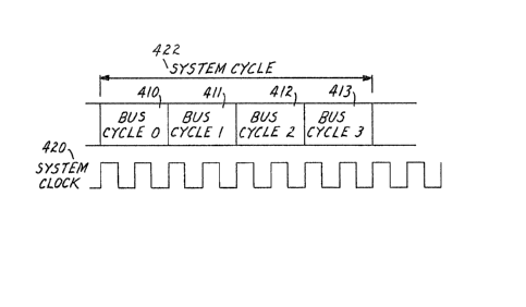
A bus cycle on PA bus 34 is the equivalant of two
system clocks, as illustrated in Figure 4. ~ bus cycle is the
duration that a single addre~s is resident on PA bus 34.
A system cycle 422, as shown in Figure 4 is a time
period that is four bus cycles (410-413) in duration. The
system cycle (422) defines the periodicy of PA bus 34. Each
bus cycle (410-413) of the system cycle (422) is designated
as Bus Cycle 0 (410), Bus Cycle 1 (411), Bus Cycle 2 (412),
or Bus Cycle 3 (413~.
The components which use the PA bus 34 are either
PA masters or PA slaves. A PA master is the source of data on
PA bus 34. A PA slave is the recipient of data on PA bus 34.
All PA slave responses occur two system cycles (422) after
the system cycle (422) in which the pA master initiated the
operation.
PA bus 34 is a fixed four-to-one time division
multiplexed bus with fixed masters activated each bus cycle
(410 413) of every system cycle (422). In other words, each
PA master has a designated time slo~ (one of the bus
cycles(410 -413)) in each system cycle (422).
As shown in Figure 2A, PA bus 34 has a total of 35
lines, including 26 address lines and 9 control lines. "X"
physical address lines XPO-XP12 (210) and ~Y" physical
address lines YPO YP12 (212) are asserted by the PA master.
~hen the operation involves image memory 16, the input/output
line I/0 (222) is set by the PA master to "0". In that case,
lines XPO-XP12 (210~ define an X physical address in image
memory 16 (corresponding to the X coordinate oP ~he upper
lefthand pixel oP the desired 4x4 subimage block). Similarly,
lines YPO-YP12 (212) define a Y physical address in image
memory 16 corresponding to the Y coordinate of the upper left
hand pixel of the 4x4 subimage block.
-8-
If inputJoutput line I/0 (220) is set to "1" by the
PA master, the operation is a parameter passing operation. In
that case, lines XPO-XP12 (210) correspond to bits 0-12 on
standard bus 28, and lines YPO-YPlO (212) correspond to bits
13-23 of standard bus 28. In tha case, YP11 and YP12 (of 212)
are not used.
The not parallel address ready (NPAR) line (214) is
a control or handshake line which is asserted by the master
and is used to indicate that a valid parallel address is
present on PA bus 34. When the NPAR line (214) is "0", a
valid parallel address is present. When the NPAR line (214
is "1", this indicates that pA bus 34 is inactive.
Two system cycles after a PA master has placed a
valid parallel address on PA bus 34, the PA slave to which it
is directed is required to respond by asserting the not
parallel address detected ~NPAD) line (216) and the not
parallel address sync (NPAS) line (218). Figure 5 shows
schematically a PA master's request and a PA slave's response
(512) two system cycles later.
When the NPAD line (216) is "0", it indicates that
the address has been detected by a PA slave. When the NPAD
line (216) is "1", it indicates that an address has not been
detected.
The NPAS line (218) permits multiple PA slaves to
synchronize to a single PA master. When the NPAS line (218)
is "0", it represents a PA slave request to the PA master to
hold the address which had been asserted on the XPO-XP12
(210) and YPO-YP12 (212) lines. The PA master is required to
repeat that address during its turn in the next system cycle.
When the NPAS line ~218) is "1", it indicates that all PA
slaves are ready.
The read/write (R/W) line (220~ is asserted by the
master. A "1" on the R/W line (220) designates a read
operation, and a "0" designates a write operation.
As discussed previously, the input/output line
(I/0) (222) indicates whether the operation is involving
image memory 16 or is a parameter passing operation. A "0" on
- 9 -
~ 3
the I/0 line (222) designates the operation as involving
image memory 16, while a "ln designates a parameter passing
opera~ion~
The opera~ion mode (MODE) line (224) is also
asserted by the PA master. A ll0" on the MODE line (224)
designates a non-interlaced transfer, and a "1" indicateq an
interlace transfer. The I/0 (222) and MODE (224) lines are
used to select the format for data transferred over PD bus
36. The operation of these formats will be described in more
detail in the context of PD bus 36.
In preferred embodiments of the pre~ent invention,
image memory 16 is capable of storing multiple planes of
pixel dataO The same two-dimensional X and Y address
coordinates apply to each plane. Multiple planes are used,
for example, where three- or four-color image data has been
scanned and stored. In that case, each plane represents one
color. In a three-color application, there are three planes
which can be simultaneously or individually addressed using
the same X and Y coordinates, simply by altering the PO
(226), Pl (2~8) and PG (230) lines. The plane number lines PO
(226) and Pl (228) define a two bit number. The plane group
(PG) line (230) selects either single plane operation (when
it is ll0") or multiple-plane operation (when it is "ln). For
multiple-plane operation, the PG line (230) is "1",
indicating that all planes from "0" through the plane number
are to be addressed with the same X and Y address
coordinates.
If the PG line (230) is "0", the plane number
defined by PO (226) and Pl (228) is simply the plane to be
used for the particular operation. If the PG line (230) is
"1", the plane number designates the final plane of the plane
group to be used in that operation. The plane number lines PO
(226) and Pl (228) and the P~ line (230) are asserted by the
PA master.
Pipeline data (PD) bus 36 shown in Figure 2B
contains bit mapped image or graphics data for transmission
between components of image processor 10 and preferably is
--10--
s ~
connected to internal parameter registers of each component
for the passing of control parameters. PD bus 36 is a
tri-stated bus which is terminated at the hiqh state at its
physical start and end points.
The components which use PD bus 36 can be classifed
as PD masters and PD slaves. A PD master is a device that
controls transfers on PD bus 36. All PD mas~ers are
unconditionally in control of the PD bus during their time
slot. Each PD master must know a priori the PD slaves which
are unconditionally on PD bus 36.
A PD slave is a device that responds to a PD
master's request. A PD slave is conditionally on PD bus 36
during a time slot and is activated by a valid address
appearing on PA bus 34. Each PD slave must know internally
lS which PD bus to use for every access code on PA bus 34.
AS with PA bus 34, the operation of PD bus 36 is
defined in terms of bus cycles and system cycles. The bus
cycle (410 - 413) is the equivalent of two system clocks
(420), and there are four bus cycles (410 - 413) in a system
cycle (422). All operations on PD bus 36 take a full system
cycle (422) to occur.
All system cycles (422) occur on a pair-wise basis
on the PD bus 36. These cycle pairs (610) are broken into odd
(612) and even (614) cycles, as illustrated in Figure 6. A PD
master may be in one of four states at any instant. If both
the even (614) and odd (612) cycles are unconditionally off,
the PD master is off the PD bus 36. If the even cycle (614)
is unconditionally on and the odd cycle (612) is
unconditionally off, the PD master uses only the even cycle
(614) for data transfer. Conversely, if the even cycle (614)
is unconditionally off and odd cycle ~612) unconditionally
on, the master uses only the odd cycle (612) for data
transfer. Finally, if both the even (614~ and odd (612)
cycles are unconditionally on, the master uses both cycles
(612 & 614) for data transfer.
As shown in Figure 2B, PD bus 36 contains 40 linas
-- thirty-two lines for thirty-two bits of parallel data.
P~
PDOO-PD07 (232) define parallel data byte 0. PDlO-OD17 (234)
define parallel data byte 1. PD20-PD27 (236) define parallel
data byte 2. PD30-PD37 (238) define parallel data byte 3.
The source of the da~a for data bytes 0-3 (232,
234, 236, 238) is determined by the state of the read/write
(R/W) line (220~ of PA bus 34. If the R/W line (220) i3 "on,
the source of the data bytes is the PD master (since this is
a write operation). Conversely, if the R/W line (220) is nl"
(indicating a read operation), the source of the data bytes
on PD bus 36 is the PD slave. By using the not write byte
lines ~WBO-NWB3 (246, 248, 250, 252), either the PD master or
the PD slave (in the case of a write or read operation,
respectively) can determine whether or not particular data
bytes are to be used, modifiable on a 4x4 block-by-block
basis. If one of the not write byte lines t246, 248, 250,
252) (for example NWBl (248)) is a "0", this means that data
byte "1" is valid data~ Conversely, if NWBI (248) line is 1,
the source of the data has indicated that data byte 1 is not
to be used during this operation.
The transfer of data over PD bus 36 is in different
Eormats, depending on the state of the I/0 and MODE (224)
lines of PA bus 34. If the I/0 line (222) is "1~, the
thirty-two bits of data appearing on lines PDO-PD7 (232),
PDlO-PD17 (234), PD20-PD27 (236), and PD30-PD37 (238) remain
constant over the entire system cycle (432). This is a
parameter passing operation, and the address appearing on PA
bus 34 is derived from standard bus 28.
When the I/0 line (222) is "0" meaning that the
operation involves image memory 16, the thirty-two bits of
30 data appearing on PD bus 36 are updated every bus cycle (410
- 413) within the system cycle (422).
The MODE line (224) of PA bus 34 selects whether
the thirty-two bits data transferred when the I/0 line (222)
is "0" are in the form of a 4x4 pixel contiguous region or is
in the form of a 2x8 pixel interlaced region. Figure 7A shows
the 4x4 subimage block (710) which is passed when the MODE
line (224) is "0". This is the standard subimage block (710)
l2 ~ 3
used for transferring data over pipeline bus 30. Figure 7B
shows the 2x8 interlaced region (712) which is transferred
when the MODE line (224) is "l".
The remote data enable tRDE) line (254) of PD bus
36 is used for communication with a remote slave through
input interface 14. When the RDE line (254) is "0" and the
R/W line (220) of PA bus 34 is "0" the PD master asserts data
over PD bus 36~ Conversely, if the RDE line (254) is "l" and
the R/W line (220) of PA bus 34 is "l", the PD master
receives data from the remote slave over PD bus 36.
PD bus 36 includes three handshake lines: the not
parallel data ready (NPDR) line (240); the not parallel data
accepted (NPDA) line (242); and the not parallel data ~ync
(NPDS) line (244). The states of these three lines during a
typical system cycle is illustrated in Figure 8~
The NPDR line (240) is asserted by the PD master
and indicates whether or not the PD master is ready to either
accept data or to transmit data. A "l" on the NPDR line (240)
indicates that the PD master is not ready, while a ll0"
indicates that the PD master is ready.
If the PD slave has accepted the data or has placed
valid data on the data lines of PD bus 36, it will cause the
NPDA line (242) to drop from "l" to "0". A "1" on the NPDA
line (242) means that the PD slave has not accepted data or
25 has not placed data on the data lines. Because the NPDA
signal (242) is a pulse, in the pipelined architecture of the
present invention there is time to either place new data on
the PD bus 36 at the next Bus cycle (410 - 413) or to repeat
the same data again. As shown in Figure 8, the PD master
30 always asserts the NPDR line ~240), and the PD slave always
asserts the NPDA line (242) at the appropriate bus cycle time
(e.g. Bus cycle 2 (4l2)~ to allow the PD master to react to
the status.
If any component on PD bus 36 determines that it
35 wants to abort the data transfer for any reason, it drops the
NPDS line (244) during Bus cycle 2 ~412). Either a PD master
or a PD slave can assert the NPDS signal (244). As long as
-13~ J ~
~he NPDS (244) line is "1" all components are ready for data.
If the NPDS line (244) is 1l0ll, this constitutes a request by
the asserting device that the PD master hold the data for
this system cycle and (422) repeat it the next valid system
cycle (422).
This is particularly important where there are
multiple PD slaves on a given PD bus 36 at one time. If any
PD slave feels that it i5 not prepared Eor a particular
transfer, it can drive the NPDS line low (244) ("0") and
essentially abort the whole system cycle (422) for all
components. Once all o the components agree that they are
ready for the transfer of data, the NPDS line (244) will
remain "1" for the entire system cycle (422) and the system
cycle (422) will proceed normally. This forces a
synchronization on PD bus 36 so that all transfers are always
completely valid transfers of data regardless of the number
of PD slaves on the PD bus.
As shown in Figure 2C, master timing (NT) bus 38
includes system clock lines SCLK+ (256) and SCKL- ~258), a
master sync (MSYNC) line (260), and a system initialize
(SINIT) line (262). SCLK~ (256) and SCKL- (258) are positive
and negative polarities of a differential ECL system clock
signal which, in a preferred embodiment, operates at 20 mHz.
The MSYNC signal (260) shown in Figure 9A, dictates the
beginning of a timing cycle.
The SINIT signal shown in Figure 9B (262) is an
initialization signal for the entire system. Normally, the
SINIT signal (262) is "1". When an initialization is to take
place, SINIT (262) is "0" for two system clocks (420).
3. Address Generator 18
In the embodiment of the present invention shown in
Figure 1, address calculation and generation and data
calculation are performed separately in address generator 18
and intensity processor 20, respectively~ In order to
maintain high throughputs with a pipeline architecture, image
~ . "? '`. ~," ~
-14-
processor 10 of the present invention preferably pipelines
both address calculations as well as data calculations. As a
result, the genera~ion of addresses is not a limiting factor
in high speed operation.
As described previously, PA bus 34 has a free flow
characteristic, meaning that an address placed on PA bus 34
is assigned to a time slot in the pipeline. If that address
cannot be immediately accepted by image memory 16,
handshaking takes place which allows ~he same address to
again be placed on PA bus 34 at the next occurrence of its
time slot. This may be repeated as many times as required for
the address to be accepted. This free flow characteristic,
therefore, effectively results in starting and stopping of PA
bus 34.
Figure 10 shows a preferred embodimen~ of address
generator 18, which is a pipelined address generator having a
stop/start capability so that it is compatible with the free
flow characteristic of pipeline bus 30.
In the embodiment shown in Figure 10, address
generator 18 includes address pipeline 40, first-in,
first-out tFIFO) buffer 42, functional address generator 44,
and control 46. Address pipeline 40 generates addres-~es at a
high rate of speed through a pipelined architecture, and may
be stopped on demand by control 46. Addresses are calculated
parametrically by address pipeline 40 and are supplied to
FIFO buffer 42, which interfaces with the address lines of PA
bus 34. FlFO buffer 42 is a first-in, first-out memory that
absorbs the speed variations between the starting/stopping of
PA bus 34 and the starting/stopping of address pipeline 4D.
Control 46 interfaces with the handshake lines of PA bus 34
and provides control signals to address pipeline 40, FIFO
buffer 42, and functional address lookup table 44. When the
PA bus 34 stops and FIFO buffer 42 begins to fill, control 46
halts address pipeline 40~
Address pipeline 40 includes parameter generator
48, S T U registers 50, world image space calculator 52, X Y
Z registers 54, subimage sequencer 56, address limiter and
-15-
address builder 58, and memory management unit (MMU) 60.
The head of the address pipeline is parameter
generator 48. This is where addressing coordinates S, T and U
are calculated by an additive process. In the embodiment of
address generator 18 shown in Figure 10, parametric
calcula~ion of addresses is performed directly, rather than
by an accumulative technique used in prior art image
processors. By direct calculation, each address i~ calculated
separately, without reliance on previous addresses. As a
result, no accumulated errors are produced.
Parameter qenerator 48 passes ~he S, T and U
parameters which it has calculated to S T U registers 50~
World image space calculator 52 draws the S T U coordinates
from registers 50 and converts them to X Y Z coordinates (as
15 needed) by use of parametric equations calculated by a
multiply and add process. The output of world image space
calculator 52 is stored in x Y Z registers 54.
The output of X Y Z registers 54 is supplied to
subimage sequencer 56, where an M x M block of addresses are
20 constructed around the (X Y Z) base address by a counting
process. The X Y Z coordinates are not memory locations, but
rather are logical addresses. Subimage sequencer 56 allows
the address pipeline 40 to create a subimage which, rather
than being a 4x4 block, may be 8x8, 12x12 or 16x16 pixels
25 depending on the particular operation to be performed.
Address limiter and address builder 58 separate the
X Y Z address into required and nonrequired bits. The
required bits are arranged to build a two-dimensional or
three-dimensional virtual address. The nonrequired bits are
30 combined to form an overflow detection feature.
MMU 60 is preferably a lookup table where the
virtual or logical address from address limiter and address
builder 58 is mapped into a physical address space within
image memory 16. The output of MMU 60 is a physical address
which is supplied to FIFO buffer 42 and ultimately on to PA
bus 34.
Functional address lookup table 44 also uses the X
Y Z coordinates from registers 54 to produce a functional
-16- ~ ~ , 7 ,~, ~
address on functional address bus 32. This functional address
is supplied to intensity processor 20 and are used to select
filter coefficients used by intensity processor 20 (as will
be described in further detail later). The rate at which
S functional address bus 32 is supplying functional addresses
can vary ~rom the rate of PA bus 34. In preferred
embodiments, however, intensity processor 20 has a FIFO
buffer for receiving functional addresses, so that the
functional addresses supplied by address generator 18 over
functional address bus 32 correspond to data being supplied
to intensity processor 20 over pipeline bus 30.
Address generator 18 shown in Figure 10, with it~
parametric pipeline address generation, is capable of
performing very complex address generation functions without
speed degradation. It also allows PA bus 34 to operate at
whatever speed is required, without any loss of pixel data or
address data or any reduction in the functionality of the
address calculation functions. This interfacing is achieved
through FIFO buffer 42 and control 46 together with the
handshake lines of PA bus 34O
The particular address generation which is
performed will, of course, depend upon control commands from
microcomputer 12 which are received by address generator 18
over standard bus 28. These command load registers (not
shown) define coefficients, upper and lower bounds of
parameters, and parameter increment values used by address
pipeline 40 in the calcuIation of coordinates, and ultimately
of the addresses which are supplied over PA bus 34.
4~ Image Memory 16
Figure ll is a functional block diagram of
image memory 16, which functions as a pipelined image memory
tile. In the embodiment shown in Figure ll, image memory 16
includes pipeline address input registers 62A and 62B,
address cache 64, DRAM memory 66, holding register 68, and
data ports 70A-70F. In this embodiment, image memory 16
-17~
interfaces through input registers 62A and 6~B with two PA
buses 34A and 34B, respectively. Through output data ports
70A-70F, image memory 16 interfaces with six PD buses
36A-36F, respectively.
Pipeline address received from address generator 18
over PA buses 34A and 34B are received by input registers 62A
and 62B provided to address cache 64. In a preferred
embodiment, address cache 64 is a first~in, first-out type of
memory. When address cache 64 fills so that there are too
many addresses, it refuses further addresses over PA buses
34A and 34B. All addresses are examined an either ignored,
; accepted (entered into address cache 64), or rejected with a
repeat request using the NPAS line of PA bus 34A or 34B to
indicate a not ready condition.
If a read operation is to be performed (as
indicated by the R/W line of PA bus 34A or 34B), addresses
from address cache 64 are read into DRAM 66 where they are
adjusted for spatial continuity. A sixteen-pixel word in a
4x4 square configuration of spatially contiguous pixels is
loaded into holding register 68. Once in holding register 68,
the 4x4 pixel bIock is placed out on one of the six PD buse
36A-36F using the format described in Figure 7A.
During a write operation, data representing a 4x4
pixel block is taken from one of the data ports 70A-70F and
loaded into holding register 68. An address from address
cache 64 is then loaded into DRAM array 66 and adjusted for
its spatial continuity to select the 4x4 pixel block into
which the data is to be written.
The free flow characteristics of pipeline bus 30 is
reflected in the operation of image memory 16. If the PD bus
36A-36F has slowed down due to handshaking, data will not be
entering or exiting holding register 68 at as high a rate.
This slows down the use of addresses from address cache 64.
Since address cache 64 is not using addresses as rapidly, it
will fill and begin rejecting further addresses on PA buses
34A and 34B so that PA buses 34A and 34B begin to slow down.
In other words, handshaking on the PD buses 36A-36F will
-18- ~3~
cause a slow down of memory fetches in the memory tile which
causes a changing effect on PA buses 34A and 34B so that
there is an interrelationship between the free flowing
characteristics of the PD and PA buses.
An important feature of the image memory 16 is the
ability to transmit spatially contiguous data in the 4x4
pixel format for any address received over the PA bus
(defined by XPAO-XPAl2 (210) and YPAO-YPA12 (212)).
Conventional buses permit only addresses that are integer
multiples of the block size (or word size) of the bu~. For
example a thirty-two bit, four-pixel READ or WRITE on a
conventional bus would permit only integer multiples of four
to be received over the address bus. This can lead to severe
performance degradation in some image processing functions
because multiple READs would be required to form a region of
computational dependency. In large data base systems, such as
those typical of high resolution image processing, this must
also be valid even when the image spans multiple memory
cards, Since there is a spatial boundary between memory
cards, multiple memory cards may be required to contribute a
single 4x4 block transfer as shown.
In image memory 16 of the present invention a pixel
at X, Y comes from the memory group M, N defined by:
M = MODULO (X,4) Eq. l
N = MODULO (Y,4)
A memory tile has its memory chips organized into the sixteen
memory groups (,) through (3,3) shown in Figure 11. A memory
tile has a size defined by the number of memory chips and the
size of the memory chip (i.e., 32 256K DRAMS creates a
1024x1024 memory tile 1110). Each group (M,N) holds all of
the pixels in the memory tile that are defined by Eq. l
above, provided that X and Y are not greater than the size of
the tile. These separate pixels are held within different
locations (L) ~1112) within the memory group as shown in
Figure llA.
Spatially contiguous 4x4 subimage blocks are
read/written from the memory tile by controlling the
locations: within each group. A single 4x4 subimage block
(1120~ may draw from as many as four different locations
tll22, 1124, 1126, 1128) within the groups as shown in Figure
llB.
When memory regions larger than a single memory
tile are required, multiple memory cards (1139, 1132, 1134,
1136~ can be abutted to create an effectively larger memory
tile (1138). This larger memory tile (1138) must be
transparent to all cards (1130 - 1136) on the pipeline bus.
An example is the creation of a 2048x2048 memory region
(1138) from four 1024x1024 tiles (1130 - 1136), as shown in
Figure llC.
If a memory request requires a border region that
overlaps multiple memory tiles, each memory tile must
contribute certain pixels to the 4x4 block (1140) as if the
request was from the center of a tile This process is the
concatenation of memory tiles.
In general for a single 4x4 block (1140) up to four
memory tiles (as illustrated in Figure llC) may be required
to contribute to a single subimage block (1140) transfer,
depending on the location of the block with respect to the
boundaries of the memory tiles (1130 - 1136).
This is implemented as follows. Each memory tile
(TILE 0) (1130) decodes the PA address of itself and the
three neighbors (TILES 1-3) (1132 - 1136) adjacent to it. It
declares one of five states to exist: (1) not one of TILE 0,
(1130), TILE 1 (1132), TILE ~ (1134), TILE 3 ~1136), (2~ TILE
0 (1130) addressed; (3) TILE 1 addres~ed (1132), (4) TILE 2
(1134~ addressed, (5) TILE 3 (1136) addressed. If condition
(1) is declared this memory tile does not participate in the
operation. If one of conditions (2)-(5) exists the memory
tile must decide if it will be required to contribute to the
corresponding PD bus transfer~ This is accomplished by
examining the lower address to see if it falls within a
three-pixel border along the memory tile seams (boundaries)~
-20- ~f~ f~
If the address falls outside the three-pixel
border, then no concatenation will occur. If it falls within
the three-pixel border concatenation must occur. If
concatenation must occur, the two least significant bits
(LSB) of X, and the two least significant bits (LSB) of Y and
the quadrant are stored internally in the memory tile and
used to control the data when transmitted over the PD bus.
The PD bus is controlled as follows:
If concatenation must occur, image memory 16
decodes the quadrant, the X LSBS, the Y LSBS and the bus
cycle (0, 1, 2, 3) on the PD bus to identify which bus cycles
and bytes the memory tile must be ON (contributing to the
transfer) or OFF (letting another memory tile contribute to
this transfer). This circuit causes the PD bus memory
concatenation in such a way the receiving master device
perceives no difference on the PD bus. The NPDS line is
dropped if image memory 16 is not ready to contribute its
data.
S. Intensity Processor 20
Figure 12 is a functional block diagram of
intensity processor 20. In this embodiment, intensity
processor 20 is a circuit that performs pipelined image pixel
intensity computations using adaptive finite impulse response
(FIR) filtering. By changing filter coefficents, a wide
variety of different intensity computation operations can be
performed.
In the embodiment shown in Figure 12, intensity
processor 20 has four input ports (functional address input
port 72, I2 port 74, Il port 76, and TAG port 78) and one
ou~put port 80. Image processor 20 includes I2 buffer 82, Il
buffer 84, TAG buffer 86, control RAM 88, I2 functional
memory and coefficient s~ore 90, Il functional memory 92,
subimage scanner 94, adap~ive FlR 96, accumulator 98, outpu~
functional memory 100, and output buffer 102.
The Il (1210), I2 (1212) and TAG (1214) inputs are
bit-mapped images received from image memory 16. All three
- -21~
inputs can be generated simultaneously with the same address
from address generator 18 to image memory 16, or may be
generated separately and transmitted over three of the four
address channels on the PA bus without sacrificing
throughput. In other words, Il (1210), I2 (1212) and TAG
(1214) represent diferent planes which can be addressed. The
input images Il (1210), I2 (1212) and TAG (1214) are received
over three separate PD buses 36A-36C in subimage blocks with
a 4x4 pixel square geometry. These subimage blocks are
concatenated together to form larger subimages and then are
fed into an arithmetic pipeline.
The func~ional address input is received over
functional address bus 32 from address generator 18 and
shares I2 buffer 82 with I2 port 74. The functional addresses
select filter coefficients to be used by adaptive FIR filter
96. Filter coefficients that change with time are loaded into
I2 functional memory and coefficient store 90 (which is
implemented in a preferred embodiment as a look-up table) and
are selected by the functional address (which is different
depending on the address in the image).
The TAG image (1214) is fed into control RAM 88
that selects coefficients (tap weights) to be applied to the
Il (1210) and I2 (1212) images~ In other words, the TAG input
(1214) allows the intensity processing operation to vary on a
pixel-by-pixel basis. The selection of coefficisnts by the
functional addresses can also be affected by the TAG inputs
(1214) through control codes supplied by control RAM 88 to
store 90.
Il function memory 92 and I2 function memory and
coefficient store 90 are preferably look-up tables which
perform preprocessing of the Il tl210) and I2 (1212) images
received from buffers 84 and 82, respectively. The particular
function memory page of the look-up table used for
preprocessing is based on control codes from control RAM 88,
which are selected by the TAG inputs (1214). A typical form
of preprocessing performed in FM 90 and FM 92 is gray scale
transformation.
22 ~ q~
~ J
The subimage scanner 94 reads pixels in the region
of computational dependency and inserts them into the
pipeline through control RAM 88 in a sequential fashion. This
allows variation of filter size weights based on
computational dependency of surrounding pixels.
The arithmetic pipelines for I and I2 merge at
adaptive FIR filter 96 where arithmetic and logical
operations are perormed and the results accumulated in
accumulator 98. In the block diagram, FIR 96 include~ a
combiner for performing what may be termed "post filtering"
combiner functions such as add, subtract, multiply, divide,
OR, XOR and A~D. These combiner functions are selected by
combiner codes from control RAM 83 based on the TAG inputs.
The final results are passed to output functional memory 100
and are stored in output buffer 102. Output buffer 102 acts
as a first-in/first-out memory and permits pipelined
intPnsity computations to occur. Upper buffer 102 is
connected, through upper port 80, to pipeline data buses
36A-36F.
By using adaptive FIR filtering, function memories
for preprocessing, and an arithmetic and logical combiner for
postfiltering functions, intensity processor 20 is capable of
performing a wide variety of different intensity processing
computations which are selectable by address generator 18
under the control of microcomputer controller 12 and by the
TAG inputs (1214). All that is required to change from one
type of image processing to another is simply to change the
coefficients or tap weights to the adaptive FIR filter,
function memory pages, and/or combiner codes. These tap
weights, function memory and combiner codes can be changed
through the functional addresses produced by address
generator 18, and also are varied by the TAG input.
6. Display Formatter 22
Figure 13 shows a preferred embodiment of display
formatter 22, which converts pipelined image data which is
encoded in a square 4x4 pixel format frorn pipeline bus 30 to
asynchronous serial (line-by-line) video signals suppliad to
video display 24. Display formatter 22 decouples the output
timing supplied to video display 24 from the input or system
timing of pipeline bus 30. As a result, pipeline bus 30 can
operate on a stop/start free flow basis without interfering
with operation of video display 24.
As shown in Figure 13, display formatter 22
includes a pair of double buffered address converter RAMS
104A and 104B. Subimage block pixel data is received from
pipeline bus 30 by buffers 106A and 106B which are associated
with RAMs 104A and 104B, respectively. The outputs of RAMs
104A and 104B are supplied to buffers 108A and 108B,
respectively. The outputs of buffers 108A and 108B are
provided to D/A converter 110, and the ou~put is an analog
video aigna which is supplied to video display 24.
The control circuitry for display formatter 22
includes write select circuit 112, and address select
circuits 114A and 114B.
Buffers 106A and 106B are operated using the system
clock ~420) provided by pipeline bus 30O One of the RAMs 104A
or 104B ls being written into using system timing produced by
the system clock t420j, while the other RAM is being read out
using the timing tvideo clock tll6)) of video display 24. The
RAMs are reversed after a given length of time tfor example
four video lines) sufficient to allow both input and output
completion.
For example, during a time when RAM 104A is being
written into, the wri~e A signal (1306) is being supplied to
RAM A t104) and the address is being supplied from address
select 114A to RAM 104A at a rate determined by ~he ~ystem
clock t420). The starting address tl310~ is the input address
supplied to address select circuit 114A, and subsequent
addresses are provided at the system clock t420) rate.
At the same time, RAM 104B is being read out by
addresses from address select circuit 114B. The starting
address is supplied by the output address t1312) input to
~ 3 ~
-24-
address selec~ circuit 114B, and the addresses supplied to
RAM 104B are changed at the video clock rate.
As data is being read from RAM 104B into buffer
108B, the previously read out data from RAM 104A which is in
buffer 108A is being supplied to D/A converter 110 at the
video clock (116) rate.
Display formatter 22 provides a number of
significant advantages. First, by decoupling output timing
from input timing, small time variations between pipeline bus
30 and video display 24 are permitted without having an
adverse effect on one another. For examplel variations in
video timing as required for GENLOCK video capability is
permitted without affecting system timing of the pipeline bus
30.
Second, dislay format 22 allows pipeline bus 30 to
stop and start independently of video burst requirements as
long as the average data rate is maintained over the swapping
time of RAMs 104A and 104B. This permits utilization of
horizontal blanking time for writing.
Third, display formatter 22 provides a conversion
from subimage block pixel configurations (which are highly
efficient for transferring image data on pipeline bus 30 to a
data format which is compatible with normal operation of
video display 24 (such as a line-by-line raster scan format).
7. Conclusion
The image processor of the present invention
provides a highly efficient, adaptable~ and high speed image
processing architecture. The pipeline bus 30 of the present
invention permits free flow data transfers so that a wide
range of image processing functions of varying computational
complexity can be performed.
The subimage block configuration used to transfer
image data over pipeline bus 30 offers significantly
increased speed and efficient addressing since only a single
address needs to be provided in order to obtain an entire
block of pixel data.
-25-
The parametric, pipelined, direct calculation of
addresses in address generator 18 also offers high speed and
accuracy. The use of adaptive FIR filtering for all intensity
processing operations lends itself ideally to a high speed
and highly flexible system- Finally, the asynchronous
operation of display formatter 22 allows a free flow pipeline
bus architecture while providing video display capability.
Although the present invention has been described
with reference to preferred embodiments, workers skilled in
the art will recognize that changes may be made in form and
detail without departing from the spirit and scope of the
invention.
., ,. , I