Note: Descriptions are shown in the official language in which they were submitted.
1 3 1 23~3
--1--
~;pike TraIl~mi~sion for Neural Network~
BA(~KGROUNlC! OF THE INVENTION
I. Field of I~e~tion
This invention relates in general to an improved method of performing
5 Back Propagation in the training of Neural Network~, and more specifically to
a method utilizing pulse trains as the information transmittion mecha~ism
within a Neural Network.
II. B~ckground A~rt
A~ used herein, a neural network performs a mapping from input data
10 to output data, ie.: it receives a set of inputs, in some form, from an external
source and from them produces a set of outputs, in some ~orm. A normal
computer i~ a typical device which performs just such a function. A Back
Propagation Neural Network is supposed to learn or adapt to perform the
mapping by bein~g given stereotypical examples of wha~ it is supposed to do.
15 This i8 in constrast to a normal computer which must be told how to perform
a mapping function.
Jmplementing Neural Networks in I~tegrated Circuits (IC) is desirable.
One of the ma,ior difflculties in implementing a neural network on an
- IC is that, in the theoretical ideal, a neural network is inherently an analog
20 process which necessitate~ a great number of analog components, including
~; analog multipliers. Conventional Neural Networks, and Back Propagation
Neural Networks in particular, which use analog methods, are quite sensitive
to O~set Errors. Off~et Errors are a particular kind of inaccuracy inherent in
analog multipliers (and analog amplifiers in general). Analog multipliers, in-
25 stead of giving the desired Z= AxB, give instead
~ = (A ~ Offset,~ ) x (B ~ Offset~) + Offsetz. Because of the offset errors, a Net-
work often is unable to converge to a reasonable answer, and therefore cannot
learn to per~orm the desired mapping function.
1 3 1 2383
-2--
Also, the Back Propagation algorithm utili3es an almost arbitrary,
non-linear function and its derivative. The~e two functions mu~t be farily ac-
curate, lest the algorithm i8 not able to learn. Implementing the3e two func-
tions with the required accuracy can be difficult.
This invention di~closes a ~amily of physical device~ that overcome
these problems.
Original theoretical approache~ towards neural networks a~e based
upon the idea that when two neurons in the brain are active there i8 a correla-
tion between them. One early rule developed by D. O. Hebb i8 described in
his book ~'The Organization of Behaviour", Wiley, lg48. The Hebbian rule
~tates that when two neurons are firing ~imultaneously an association link
between them is strengthened. Accordingly, the next time either of the two
neurons fires, the other one is more probable to ~re also. However, the Hebbi-
an rule is not a sufflcient model to explain the learning proces~. Under the
Hebbian rule, the connection strength~ between neurons grow without bound.
~ maximum~ are placed on the connection strengths, these maximums are al-
ways reached.
Subsequently, the Perceptron Model WaB developed by Fr2nk Rosen-
blatt, and is discus6ed in hi~ book "Principles of Neurodynamics", ~partan,
1962. The Perceptron Model was originally believed powerful enough to en-
able a machine to learn in a huma~-like manner.
The Perceptron Model include~ inpllt, hidden and output layers; each
compri~ed of one or more processing elements. In response to input stimuli,
the input layer provides information to the hidden layer. Similarly, the hid-
den layer provides information to the output layer. Connections between the
input and hidden processing elements are fixed; connections between the hid-
den and output processing elements are adjustable.
In the Perceptron Model, if the inputs are boolean (i.e. either zero or
one~, then the intended purpose of the hidden layer is to extract some kind of
features from the input data. However, if the inputs to the Model are con-
tinuou3 numbers (i.e. having more than two distinct values, rather than just
two boolean ralues), then the hidden layer iB not used. Instead, the outputs
of the input layer are connected directly to the inputs of the output layer.
1~ the Perceptron Model, all learning takeR place in the output layer.
Under the Perceptron Model many problems have been experimentally and
1 3 ~ 2383
3-
mathematically shown to be repre~entable by connection strengths between
layers. Rosenblatt's Perceptron Learning Algorithm enables a neural network
to find a solution if there exists a representation ~or that problem by some setof connection strengths. Rosenblatt's Perceptron Convergence Proof is a well
5 known mathematieal proof that a Perceptron Systern will find a solution if it
exists.
In operation, the Perceptron Model modifies the strengths of the
weighted connections between the processing elements, to learn an appropri-
ate output re~ponse corresponding to a particular input stimulus vector. The
10 modification of the connection weights oecurs when an incorrect output
response is given. Thi~ modification of the weight~ changes the tra~sfer OI in-
formation from the input to output processing elements 80 that eventually the
appropriate output response will be provided. However, through experimen-
tation, it was discovered that the Perceptron Model was unable to learn all
15 possible functions. It wa~ hoped that these unlearnable functiQns were only
pathological cases, analogous to certain problems that humans cannot solve.
This is not the ca~e. Perceptron Systems ca~not represent and learn some
very simple problems that humans are able to learn and represent
An example of a problem that the Perceptron Model is unable to
20 represent (without 2~ hidden proce~sing elements, where N is the number of
input nodes), and therefore cannot learn, is the parity or ~'exclu~ive-or~' boole-
an function. To per~orm such a problem (with fewer than 2N hidden process-
ing elements) a system would require two layers of modifiable weights. The
Perceptron System cannot properly adjust more thMl one layer of modifiable
25 weights. ~t was speculated that no learning mechanism for a sy~tem with
multiple layers of modifiable weight~ would ever be discovered because none
existed (Mins~y & Papert, 19~, in l'Perceptrons").
(The problem with using 2N hidden units is three-fold. First, since the
hidden unit~, in the Perceptron Model, do no$ adapt, all the units must be
30 present, regardless of the function which needs to be learned, so that all func-
tions can be learned. Second, the number of u~its required grows phenome-
nally; for example, 234 is approxi$rlately 17 billion, more neurons than in a
human brain; this means that the largest parity problem the human brain
eould solve, if wired in this m~ner, would ha~re at most 32 inputs. Third,
35 the aystem would not generali~e; given two input/output vector pairs near
one another, one trained and the other not, the system ~hould be able to in-
1 3~ 2383
-4-
terpolate the an3wer from the first; with a large number of hidden units, it
ha~ been experimentally shown that this is not the ca~e.)
Almost all adaptive neural ~ystems share several ~eatures in common.
Typically the processing elements of all ~ystem3 have an output which is a
5 function of the sllm of the weighted inputs of the processine element. Almost
all syætems llave a single layer of modifiable weights which affect the data
tranæferred from the input to the output of the system.
The eYolution of adaptive neural systems took a dramatic step forward
with the development of a~ algorithm called "Back Propagation". This algo-
10 rithm iæ fully described in the reference text '~Parallel Distributed Processing,the Microstructure of Cognition~', Rllmelhart, Hinton,& Williams, MIT Press, 198~.
A back propagation system typically consi~ts of three or more layer~,
each layer consiæting of one or more proce~sing elements. In one basic exam-
15 ple, the system i8 comprised of an input layer, at lea~t one hidden layer andan output layer. Each layer contains arbitrary, directed connections from the
proceææing elements in the input layer to the hidden layer, and from the hid-
den layer to the output layer. There are no connections from processing ele-
ments to processing elements in the ~ame layer nor connections ~om the out-
20 put to the hidden layer nor from the hidde~ to the input layer; i.e. there areno cycles (loops) in the connection graph. (There are hypotheæized mechan-
isms for networks with cycle3 in them, but they ~re not bei~g æcrutinized
herein.)
In the Perceptron Model the idea of error W&S introduced. In a back
25 propagation 8y8tem, at each output processing element of the networl~, the er-
ror is quite easily reali2ed. The error is typically the difference between an ex-
pested Yalue and the output value. This error iæ used to modify the strength
of the connection between a processing element and the output processing ele-
ment. Ideally, thi~ reduces the error between the expected output and the
30 value output by the procesæing element in response to the input. The Percep-
tron Model lacks the ability to allocate an error value to the hidden proce3s-
ing elements and therefore c2nnot adjust the weights of any connection3 not
coupled to an output processing element. I~ a system utili~ing the Back Pro-
pagation algorithm, an error i8 assigned to the proceææing elements in hidden
35 layers and the weights ~ the connections coupled to these hidden proce~ing
elements can be adjuæted.
I
1 3 1 2383
An acyclic Neural Netwo~k is comprised of only three layers of process-
ing elements: the input, the hidden and the OUtpllt layers. Each layer consists
of one or more proce~ing elements. There may be connections from the input
to the hidden layer (input matrix elements), from the hidde~ to the output
layer (output matri~t elements), ~rom the input to the output layer ~direct ma-
trlx elements~, and from hidden processing elements to other hidden process-
ing elements (hidden matrix elements). In an acyclic network, a la~ge con-
straint is placed on hidden matrix elements: if the hidden proce~sing elements
are numbered 1 to N, a matrix element may only comlect from a lower num-
bered hidden processing element to a higher numbered processing element;
remember that the directionality of a matrix element is important.
This thre~layer description actually produces all possible layered en-
vironments; it describes an acyclic graph.
An acyclic Back Propagation Neural Network con8ist8 of the following.
A neural ~ystem utili~ing backward~ error propagation can be
represented by two kinds of elements: processing elements and matrix ele-
rnents.
A matrix element connects two processing elements and its primary
function is to store the connection strength.
A processing element receives a net data and a net error signal, and
produces a data and an error signal, which are function~ ~ the two received
signals. The function~ can be mathematically expre~ed as:
(1)
Outputj = f ( Nettnputj )
Error; = f '( J~ctInputj )xNetError;
A matrix element receive~ a data and an error signal and produces a net data
and a net error sigllal which a~e a function of the two received slgnals. The
functions can be mathematically expressed a~:
NetInput, = ~ Wei~htjixOutputj (3)
~ i
~ NetErrorj= ~ WeightjixOutputj (4)
,
dtj = Learn Ra~ejjxErrorjxVutputj . (S)
The derivation of the discrete time Back Propagation Algorithm i~
described in Chapter 8 of PaJallel Distributed Proees~D, by Rumelhart et al,
5 and is recounted here.
A weight a~sociated with a connection i~ referred to as U~j,. The sub-
~cripts are used in the form Wto~from~ Eence~ in the Yariable wji, i refers to the
proce~sing element from which data information is being received, and j refers
to the processing element to which data information is sent. In the back pr~
10 pagation algorithm, a particular input stimulus vector i8 referred to collec-tively by the ~ariable p ~for pattern~. The element~ of a pa~ticular output
vector aDd particular target vector are referred to respecti~ely a~ op~ d Tp;,
where j varie~ over the output processirlg elements. The Total Error of a sy~
tem is repre~ented by the variable E. The portion of the Error contributed by
15 a ~ingle input vector (one input pattern) i8 represented by the variable Ep.
The output of a processing element op;, in response to an input pattern
p, is is calculated by the following equation (which also defines the Yalue
netp;):
netpj= ~ Wj; op, ~6)
(7)
Op; = f(netpj)
The techniques used by Back Propagation to minimize the Total Error is a
variant of Least Mean Squared. The technique states that the total error is
the square of the difference between the target vector and the output vector.
Furthermore, it ii assumed that the total error for the system is the linear
25 summation of the error for any indiiritual pattern.
E= ~ Ep (~)
Ep = 2 ~ (Tpj - opj)2 (9)
In a Back Propagation network, erTor is minimized by adjusting the weights
within the network. What is de~ired i~ to determine what amount to adjust a
30 weight 80 that the error will be reduced. The ~ollowing equation expresse~
that desire:
1312383
aw~ aWji
The above expression can be expanded by the chain rule to get:
awji = ~ ~ an~t~ ~j; (11)
5 We can expand the second component, a '~, by noting that
netp/~ = ~ w/~mom, to get the following
Wkmnm)
an~t7~ m (12)
It i8 easy to see that except when m=i and k=j, the above i~ zero. Putting
this back into equation (11) we get:
10 awji = ~ an~tni (13)
The first portion of the equation, ~, by expansion using the chain rule,
gives:
aEp _ ~ a~p ao", (14)
anetpj , aop, anetpj
and a t~l ca~ b~ simplified by recognizing op, = f(netp/). By sub3tituting
15 this in, the expres~ion becomeff:
aop, af (ne~p/) (15)
~netp; anetp;
It can now be noted that ~!~ is ~ero, e~cept when l=j; this gives us
finally:
anctpj anet j = f'(7~e~pj) (16)
20 and this can be substituted back in to get:
f 3 1 2383
awjj = ~ aOPjf'(n~tpj)Oi (17)
If we are examining an output node, the value of aoP i~ readily apparent
from the definition of Ep, a~ in:
13p = 2 ~ (Tpj--Op~)~ (18)
Partial di~erentiation of this expression with respect to Opj gives the follow-
ing expres~ion for output processing element~:
aEp
ao = Tpj- Opj (lg)
Thus the error equation for an output value i8:
o a P = (TP~ pj)f'(netpj)oi (20~
The problem remains what the er~or vallle i~ for the hi~den processing ele-
ment~. To determine this, let the definition of V~pj be:
aEp
Pj ~nctpj (21)
From the expan~ion from above, we ~ee:
aEp a~
a~C~p; a~ f (netpj) (22)
ExpandiDg by the chain rule on opj, we get:
aEp _~ anetp~
r~etp~ aOpj (23)
Expanding a "', by the definition netp~; = 2 Wkll, we get:
anetpk a(~ Wklp~)
aopj = aopj (24)
20 It i~ ea~y to see that the above is zero, except when l=j, ~o that we can state:
1 3 1 2383
anOtp~ awtjOpj (25)
Substitu$ing thi~ back into the above equation, we get:
aO Pj = ~ ( anctP~ wkj) (26)
5 By the definition of f~pj, we can then state:
~30 j ~ (~pk Wkj) (~27)
Therefore, tipj for a hidden node can be expre~sed as:
~Cpj = f ' (netpj)~ (~p~W~j) (28)
Combining all the above elements together, we get:
awj, ~Pi P; (29)
and from thi~, the Total Error equation can be formulated:
aaE = ~ ~pj Opj (30)
For an output proce~sing element, ôpj i9:
~pj = f ' (netp;) ( Tpj--Opj) (31)
15 For a hidden proce~sing element, ~pj iS:
~Pj = f (n~p~ p~CWkj) (32)
Now, t~e change of the weight is set proportional to the above partialdifferentiation. This i~ given by the following equation:
VW~ pjopi (33)
The con~tant of proportionality (~6) is the Learn Rate. Experimentally,
this con~ta~t ha~ been foulld to be in the range of .5 to very ~mall, depending
on the number of weights, proce~ing elements and patterns which are to be
pre~ented.
Note that there i9 no guarantee that ally one particular weight change
for a particular pattern will decrea3e the total error; it i~ actually quite prob-
able that during one of the pattern~ the total error will increase, just that
t3~2383
-1~
over all the pattern~ the total error should decrease.
Ill 8umma~, back propagation may be described as follows. On a for-
ward pass of information through the network, all of the processing element
outputs are calculated by propagating the information input forward through
5 the network, i.e. from the input layer to each hidden layer in turn and finally
to the output layer. C)n a backward pass, i.e. from the output layer to the
hidden layers, each in rever~e order from before and finally to the input layer,all the errors are calculated by propagating the associated errors backwards
through the network. Finally, all the weight~ are changed a~cording to the
10 errors in the proce~ing elements above and the outputs of the proce sing ele- ment~ below.
The Back Propagation Algorithm a~ originally developed and as
described ts) this point is a discrete time algorithm, in that there is a forward
pass, a backwards pal38 and modification to the weights, and then a recycling.
15 However, this is not an optimal implementation of the system. There is an
implicit assumption of linearity during these discrete time intervals~ This i8
generally not a good assumption.
A better implementatinn of the sy~tem i8 for the network to run con-
tinuou31y, per~orming each of the operation~ simultaneously; this is the ba~is
2û of what is called herein a continuous time system. The following iB a deriva- tion of the continuoua time model of the Back Propagation Algorithm, as
developed by this inventor. Instead of taking the derivative of the Error with
re~pect to any particular weight, the derivative i~ taken with respect to time.
It is de~ired to haYe the error monotonically decreasing, and it i~ ~hown that
25 this i8 done in a straightfoward malmer. The chain rule can be applied taking the partial differentiation with respect to wjj.
dt ~, awjj dt ( )
Repeating equation (30), as deri~ed in the discrete time algorithm:
~wj, = ~ awjP~ pjop~
30 This can then be replaced into equation (34) to gi~e:
1 3 1 2383
dt = ~ Pipi) dt (36)
To ensure that the derivative of $he Error is monotonically decreasing, the
sign of dt must b~ negative. The only way to do this is to ensure that the
5 sign of dtj is the opposite sign of ~ ~pjpi
By arbitrarily setting
dwjj
dt~ p j pi (37)
this constraint i9 satis~ed, by giving us:
d~
d =--~ pjpi) (38)
Since the deril~ative of the Error iB monotonically decreasing, the system will
converge at some final error value. A~ derived, a system is not guaranteed to
converge to a zero Error. E:xperimental results show that a system generally
will converge to zero error if the problem to be solved i8 representable by the
network. It iB not known at this time how to ~etirmine if a problem to be
solved is representable by a particular network. If the system does not con-
verge to a small error, or does not reliably converge, adding a small llumber ofadditional processing elements and comlections will lead to convergence.
Figure 1 is a diagrammatric representation of an acyclic Back Propa-
gation Neural Network, having 8iX processing elements: two input processing
elements, two hidden processing elements and two output processing ele-
ments. Thi~, of course, i8 a very small exemplary network, but from the
drawing3 and description of this representative network it can be seen that a
similar network call be constructed comprising thousands (or millions) or pro-
cessing elements.
In liigure 1, processing elements are denoted generally as 2U's with
input layer processing elements 20a and 20b, hidden layer processing elements
20c and 20d, and output processing elements 20e and 20f. As shown on pro-
cessing element 2ûe, processing elements may have four lines: two output si~g^
nal lines, Data 11 and Error lg; and two input signal lines, Net Data 13 and
Net Error 12. The post~cript "e" designated that the lines are associated with
processing element 20"e".
1 3 1 2383
-12-
Matrix elements are denoted generally as 10's. Matri~e elements 10
have data, error, net data and net error lines which are colmected to the simi-
laTly named lines of the connected proces3ing elements, as diagrammed.
The two element~ of the input vector are tran~fered respecti~ely to the
system via input stimulus 1 line 31 and input ~timulus 2 line 32, which are
connected to the Net Data lines of input proce~sing elem~nts 20a and 20b,
respectively. The two elements of the output vector are available on Output
Value 1 line 35 and Output Value 2 line 36, respectively, and are generated
by the data lines of output processing elements 20e a~d 20f, rep~ectively. The
two elements of the error vector are tran~ered re~pectively to the system via
Error Stimulus 1 line 33 and Er~r Stimulus 2 line 34, which a~e connected to
the Net Error line~ of output p~ocessing elements 20e and 20f, respectively.
Figure 2 is a schematical block diagram illustration, a matrix
~epresentation, of the layout of the ~ystem diagrammatically represented in B
Figure 1.
Processing elements 20a' through 20f' correlate with processing ele-
ments 20a through 20f, respectively, of Figure l. Matrix elements 10a'
through lOm' correlate with matrix eleme~ts 10a through 10m respectively, of
Figure lo All signal lines, 11a' through 14f' correlate with signal lines 11a
through 14i~, respectively, of l?igure 1. The input, output and error lines 31'
through 3~' correlate with the input, output and error lines 31 though 36 of
~igur~ 1.
An input stimulu~ vector, comprised of input stimuli Input 1 on line
31' and ~put 2 on line 32', are connected to proces~ing elements 20a' and
20b', re~pectively, as is done in Figure 1. The output of proce~sing element
20a' is ~onnected to matrix elements lOa' through lOd' via Data line 11a'.
Similarly3 the output of processing element 20b' is connected to matrix el~
ments 10e' through 10h' via Data line 11b'. Matrix Elements 10a' and 10e'
sum their Net Data outputs on Net Data line 13c'. Thi~ summation on 13c' is
provided as the Net Data input to processing element 20c'. Processing Ele-
ment 20c' provides its Data output signal on Data line 11c', to the Data input
line of Matrix Elements lOi' through lOk'. Matrix Elements lOb', 10f' and
lOi' sum their Net Data output signals on Net Data line 13d', which is pro-
vided as the Net Data input signal to Proce~sing Element 20d'. Processing
Element 20d' provides it~ Data output signal on Data line 11d', to the Data
input line of Matrix Elements 101' and 10m'. Processing elements lOc', lOg',
-13- 1312383
lOj' alld 101' sum their Net Data output signals on Net Data line 13e', which
is provided a8 the Net Data input signal to Proces~ing Element 20e'. Matrix
elements lOd', 10h', lOk' and 10m' sum their Net Data output signals on Net
Data line 13f', which is provided a8 the Net Data input signal to Processing
5 Element 20f'.
Proce~ing elements 20e' and 20~ provide output signals Output 1 and
Output 2, respectively, on lines 35' and 36', respectively. These outputs form
the output vector.
An er~or stimulus vector, composed of error stimuli Error~ 1 on line 33'
10 and Error 2 on line 34' are received by the Net Error line8 of Proce~sing Ele-
ments 20e' and 20f', respectively, The Error output signal ~ Processing Ele-
ments 20f' is provided on Error line 14f' to Matrix Element~ 10m', 10k', 10h'
and 10d'. The Error output signal of Proces~ing Elements 20e' i8 provided on
Error line 14e' to Matrix Element~ 101', 10j', 10g' and 10c'. The Net Error
outputs of Matrix Elements 101' and 10m' are ~ummed on Net Error 1ine 12d'
and is provided to the Net Error input line of Processing Element 20d'. The
Error output signal of Processing Elements 20d' i8 provided on Error line 14d'
to Matrix Elements lOi', 10f' and 10b'. The Net Error outputs of Matrix Ele-
ments 10i' through lOk' are ~ummed on Net Error line 12c' and is provided to
20 the Net Error input line of Matrix Element 20c'. The Error output signal of
Proce~sing E:lements 20c' is provided ou Error line 14c' to Matrix Elements
10e' and 10a'. The Net Error outputs of Matrix Elements 10e' through 10h'
are summed on Net Error line 12b' and i8 provided to the Net Error input line
of Proces~ing Element 2ûb'. The Net Error outputs of Matrix Elements lOa'
25 through 10d' are summed on Net Error line 12a' and is provided to the Net
Error input line of Processing Element 20a'.
~ n the exarnple the Error output signals of Processing Elements 20a'
a~d 20b' are not u~ed; often this will be the case, and as such a minimal sys-
tem doe~ not include the functional parts nece~sary to provide the Error out-
30 put signal of input proce~ing elements, such as 20a' and 20b', nor the ~unc-
tional parts to provide a Net Error output for the matrix elements connected
to the input processing elements. The example is provided with the Error
output signals of Proces~ing Element3 20a' and 20b' and the Net Error output
sigllal8 for MatrD~ Elements lOa' through 10h' for clarity and uniformity. A
35 sy3tem can be built in this manner with no loss of generality.
1 3 1 2383
-14-
Most Neural Networks sum the data inputs on a line and then provide
a "squa~h" of the resultant ~ummation, i.e., a non-linear function which
reduces the range of the ~ummation from the possible minus infinity to posi-
tive infinity range of the net input to some smaller dynamic ra~ge, such as
from zero to one.
J Figure 3a illustrates a typical squash function u~ed often in Back Pro-
pagation. Its mathematical formula is:
F(x)-- l (39)
1+e~
I~ a Back Propagation Neural Networ?~ the derivative of the squash
function that is used in the forward propagatio~ of the data is required to
modify the backward~ propagation of error.
Figure ~Sb illu~trates a the derivative of the function illustrated in
Figure S~a. It mathematical formula i~:
F' (2) = e (40)
(l+e~~)2
Producing hardware implementations of these functions with the required
accuracy i8 difflcult.
Prior art neural networks using the Back Propagation Algorithm have
been frequently implemented on computer systems and are now being
de~igned and built a~ fully analog VLSI circu;ta These fully analog VLSI
instantiations ~uffer from the design limitation~ of analog circuitry, in particu-
lar because of the ot~et errors of the analog circuit~. While it has been shown
that small ~etwork~ of these fully analog circuits can be built, it has not beendemonEtrated that larger networks c~ be built utilizing fully analog mechan-
isms, and it is believed by this inventor that without significant circuitry or
signficant circuitry advances to alliv;ate these offset errors, a fully analog cir-
cuit will not be able to scale up.
Therefore there exist~ a need for: a new and improved adaptive neural
network circuit design which will enable the system to overcome the
difflculties associated with analog multiplier of~set error~, and
a new and improved method for the calculation of a "squash" function
and its derivative, and
a new and improved method for the transmission of information along
neural network pathways which enhance~ the networks' immunity to random
13t2383
15-
noi~e interference.
The invention described herein i8 a family of circuits which are an
instnntiation of The Spilcc A/Iodel, after the main mechanism whereby informa-
tion i8 transferred. The Spike Model iB a mathamatical model, derived by the
5 inventor.
It i~ generally believed that a neuron tran~mits (at least part of~ the
forward ~ow of data infor~ation by representing the information a3 the fre-
quency OI the firing of spikes along its axon. Mo~t abstract neural models
repre~ent the firing frequency as a real number, rather than attempting to
10 simulate each and every individual 3pike. Most neural network models sum
the inpllts and then provide a "~qua~h" of the re~ultant sum when processing
the incoming information for a single proce~ing element. This i8 equivalent
to summing the input frequencies, then squa~hing the resultant summation.
The invention utilize~ a spike train as the primary method of forward
15 data transmission a~d extorts 3everal major advantages from it. In this
model, instead of summing the inputs, the input~ are (in e~sence) logically
OR'ed together. lf two spike~ occur simultaneously on the inputs, only a sin-
gle spike gets through. The resultant "~quash" function under this mechan-
ism is ~the assumption~ and derivations are detailed later in thi~ di~closure):
Q+ = 1-e-~ut-~ ~41)
where Q+ i8 the probability that a~ output of a unit i9 a one and net+ is
(es~entially) the total number of ~pike~ being generated by the unit~.
This fu~ction i~ approximately the upper "hal~' of the stereotypical
sigrnoid "squa~h" functions curre~tly used in most Back Propagation net-
25 works, where net + is the weighted number of excitatory spikea.
Since the number of spikes i~ exactly the summation of frequencies,thi~ giv~es not a summation of frequencie~, but rather a nice "squa~h" func-
tion, without pa~in~ for it!
One of the next maJor requirements of the Back Propagatio~ Algo-
30 rithm is the backwards flow of error. Specifically, there is a linear su~ationof the backwards flowing error and a multiplication of it by the net input
(number of spikes~ run through the derivative of the squash function, ie.:
t 31 2383
-1~
(42)
bac~wards error x squa~h~( number of spikes )
By examining the total of all the times between the pul~es, one can
find an intere~ting 3pace. The amount of this time correspond~ to:
(43)
OffTime _ 1--OrLTime
or
OffTime = ~-numb~r of Jpik~ (44)
This is exactly the derivati~e of the squa~h function (from equation 41).
Therefore, if the erxor i~ propagated backwards when no 3pikes are present (or
10 equivalently, only e~:amined when there are no ~pike~ pre~ent), the time aver-
aged multiplication i8 exactly a multiplication of the error by the derivative of
the squash function with respect to the net input -- precisell/ what i8 de~*ed!
The third component of Back Propagation i~ the way the weights are
updated. This i~ (e~sentially~:
dt~ = Output Below x Erro~ Abo1)c (45)
If the error in a node above i~ represented in a spike method, the calcu-
lation for the change of the weights i8 simple. It i8 (es~entially) the logical
AND of the fo~ward llowing ~piked data signal and the spiked error signal.
If all ignal~ in the network are repre~ented as spike~, much of the
20 noise problem~ 0ciated with pure analog signal~ i8 alleviated.
This disclo3ure derive~ various mathematical components of the model,
and detail~ va~iou~ circuits which can be utili~ed in the instantiation of this
model. It ~hould be noted that this model retain~ essentially all the speed of
a full analog implementation, in that all circuits c~ still be implemellted in
25 the p~ued~neural network. The only ~peed lost is that the frequencie~ of the
~pike~, which remain the prima~y information carrying portion of the si~nal,
can only be actually detected with substantially more than two spike~ present.
It appears that this time will need to be a factor of ten longer than theoreti-
cally anticipated with a pure analog instantiation.
~ 3 1 2383
-17-
III. Summary of ~vention
According to the invention, a neural network includes a plurality of
matrix elements, each receiving an input data value ~d producing an output
data value that i~ function of the input data value. The output data value i8
5 in the form of a ~pike train wherein the value of the data i3 represented by
the duty cycle and/or the frequency. A combining element, such as a simple
wire, produces a combining element output data value pul~e train by logically
OR'ing the matrix element output data value spike trains. ~ this simple and
elegant manner, a squash function is performed ~such as 1-e ~pu a).
10 proce~sing element receives the combining element output data value pulse
train and produces, in response thereto, a processing element output data
value, which is the time average of the combining element output data value
pnlse train.
According to another aspect of the invention, the duty cycle of the
15 matrix element output data value spike train i8 proportional to the product of
the matrix element's weight value and input data value.
The matrix element input data value may be a spike train wherein the
data value is repre3ented by a frequency. According to another a~pect of the
invention, the frequency of the matrix element output data value spike train
20 is equal to the frequency of the matrix element's input data value and the
width of the output spike i8 proportional to the matrix elements's weight
value.
ID an exempla~y embodiment of the invention, the above improv~
ments are i~cluded in a back propagation neural networ3~ that includes the
25 backward flow of error data on the combining element line. The processing
element receive~ an input error value and, in respon3e thereto and dependent
thereon, outputs an output error value as an analog value on the combining
element line during the off-time~ i.e. when no OR'ed data spikes are pre~ent.
This mea~s that only a single wire is necessary for the trasmission of both for-
30 ward data information and backwards error information between the outputof a matrix element and the input of a processing element.
A~ part of the requirements imposed by the derivation of the back pro-
gation algorithm, it is neces~ary to multiply the backward~ ~ow of error infor-
mation with the derivatiYe of the ~q.uash function. As an aspect of the inven-
35 tion it is demonstrated that the this multiplication can be performed by
~ 3 t 2383
-18-
sampling the backwards How of error information only when no OR'ed data
spikes are present on the output of the combining element.
The reason this works i8 that the off-time, computationally, i~
equivalent to e ~Ulput3, which is the derivative of the squash function. It is
5 also necessary, for the back propagation algorithm, to multiply this sampled
signal by the input data value. As a further aspect of the invention, it is
shown that this can be accomplished by sampling the above sampled signal
during the time when an input spike is present.
The bsckwards flow of error information is further transmitted back-
10 wards to the proce~sing element below the matrix element during the off-time
of the output data 3pike train from that proces~ing element below. This
means that only a single wire i8 necessary for the $r~smiasion of both forward
data information and backwards error information between the input of a
processing element and the output of a matrix element.
In another exemplary embodiment of the invention seperate transmis-
sion pathways are uRed for the forward data and backwards error information
~ow. This results in 3implified circuitry at the expense of more interconnec-
tions. In this embodiment, all transmi~sions can be performed by spike trains.
When all forward datæ and backwards er~or transmis~ions are per-
formed by ~pike trainsj the weight update call be accompiished simply by log-
ically AND'ing the complement of the output of the combining element, the
backwards ~owing error spike train,
IV. E~rief I)e~cription Of Draw~gM
The structures, objects, and advantages of the present invention will
becom~ apparent from the following detailed description, taken in conjunction
with the accompanying drawings, in which like re~erence numerals correspond
throughout and wherein:
Figure 1 i8 a diagrammatic representation of an acyclic Back Propaga-
tion Neural Network.
Figure 2 is a diagrammatic matrix representation of the Network of
Figure 1.
1372383
-1~
Figure 3a is a graphical representation of a typical squash function.
Figure 3b is a graphical repre~entation of the derivativ~ of the squash
function in figure 3a.
Figure 4 illu~trates the input and output characteristics of a Pulse
5 Width Modulator, a~ defined in the present disclosure.
Figure 5a is a block circuit diagram of a type 0 matrix ele~ent.
Figure 5b is a block circuit diagram of a type 0 processing element.
Figure ff illustrates two signal3 being logically A,ND'ed together.
Figure 7 illustrates a typical signal on a combining line of a type I cir-
10 cuit.
Figure 8a is a block circuit diagram of a type I matrix element.
Figure 8b i3 a block circuit diagram of a type I processing element.
Figure 9a i8 a block circuit diagram of a type II matrix element.
Figure 9b is a block circuit diagram of a type II processing element.
Figure 9c is a block circuit diagram of a type II proce3sing element that
accepts both excitatory and inhibitory data pulses.
V. Detailed Descr~pti~n of the Pre~erred l3:mbodiments
V.I: Forward Propa~ation via Spike Train$
According to a first a~pect of the invention, a spike train is used for
20 information tran~er in a neural network.
It i8 generally believed that a neuron transmits (at least part o~ the~orward flow of data information by representing the information a~ the fre-
quency of the firing of spike~ along its axon. Most ab~tract neural models
repreient the firing frequency as a real number, rather than attempting to
25 simulate each and every individual spike. Most neural networl~ models sum
the inputs and then provide a "squash" of the resultant sum when processing
the incoming information for a single processing element. This is equivalent
to summing the input frequencies, then squashing the resultant summation.
This invention utilizes a spike train as the primary method of forward
30 data tran mission and e~ctorts several m~or advantages from it. In this
invention, instead of summing the inputs, the inputs are (in essence) logically
OR'ed together. ~ two spikes occur simultaneously on the inputs, only a
I 3 1 2383
-2~
single spike get~ through. The resultant l1squa~h~ function under this
mechanism is (the assumptions and derivations are detailed later in this dis-
clo~ure):
~;?+ = 1_e-n~r (4~
5 where Q+ is the probability that any output of a unit is a one and net+ is
(es~entially) the total number of spikes being generated by the units.
This function i8 approximately the upper "hal~' ~ the stereotypical
sigmoid "squa~b" functions currently used in most Back Propagation net-
works, where net+ is the weighted number of excitatory spi~es.
Since the number of spikes is exactly the summation of frequencies,
this gives not a summation of frequenci~, but rather a nice "squash" func-
tion, u)ithout pavin~ for it!
In a Neural Network paradigm, often positive and negtive weight
values are allowed. It is easiest to represent only positive or negative values
15 with a pulse train, and it is ea~iest to understand the workings of this inven-
tion for the "squa~h" function by examining the e~citatory (positive) data
spikes, rather than both the excitatory and inhibitory (negative) data spikes,
associated with positive and negative weights. Two methods are disclosed
which both derive the same result. The first, recount~d in the next section
20 utilizes syncrounous pulse trains. The ~econd, recounted in the subsequent
section utilizes asyncrounous pulse trains.
V.II: Po~sson D~riu~tion of E~cc-tatory Sp~kes
By making the assumption that there are enough input~ to ~ neuron, it
is reasonable to assume a near Poisson di~tribution of the spikes reaching the
25 neuron, as a m~thematical simplification. Another derivation is given in the
next section wherein thiq assumption is not made; an identical result is
derived. This i~ an even safer as~umption if an event has just occurred, and
the neuron i8 experiencing the premier spikes triggered by the event; the
arrival of the pulse~ will primarily be timed by the interconnection strengths,
30 delay time~, etc., and not be ~actored at all by the cyclical frequency nature of
a singularly firing neuron, which is the primary debilitation of the Poisson
assumption. And furthermore, the cyclical output pulses of a neuron can be
made to occur irregularly (in a hardware implementation), with a psuedo-
random distribution equaling a Poi~on distribution. This should alleviate
1 3 ~ 23~3
21
most fears of the assumption.
Imagine now, for ~implicity that we have a system wherein these spikes
are synchronous and of unit time duration. If there are P spikes on N lines
which are being OR'ed together, in a single time sample of S time units, some
5 number of these unit time ~paces will be filled, while others unfilled. If a
large number of these ~amples are run, there will emerge an expected number
of time spaces which are filled.
From the formulas of Poisson distribution:
P[X=~,~]= !~ (47)
10 where ~ i~ the mean number of events occurring during the time interval of a
simulation. The probability PlX=~ is the probability that exactly X
e~ents will occur during that time inter~al.
(:iven a large number of spikes during a time interval, some of these
sp;kes will overlap one another. During this time, since they are being OR'ed
15 together, they will act as if they are a single spike. Hence, for a given number
of input spikes the number of apparent output spikes is given by the following
derivation:
(48)
P[X~o,~] = l-P[X=o,~]
= 1_ e A (49)
O~
= 1-e~~
While this iY a derivation for a synchmnous model, the e~ects are
readily convertible to a continuous model wherein the duration of the spikes is
variable and asynchronous. This i8 demonstrated in the lleqct section as an
alternative way of deriving the Probability for 15xcitatory Spikes.
These Probability Function3 can be translated to the forward activa-
tion for excitatory spike~. To do this, let the forward activation function be
set to the probability that the output will be a one at any given moment. Let
the symbol Q+ denote the probability that the output is one (from only the
Excitatory Pulses, and not counting the Inhibitory Pulses). Let the symbol
nvet+ denote the total number of spikes arriving during a 3ampling period.
Therefore, the al~erage probability that an output i~ one (and consequently
the forward activation function for excitatory spikes) is:
~ 3 ~ 2383
-22-
Q+ = 1 e-nct-~ (51)
V.III: In~tant~neous Pro~abilitic~ for P~2citator~ Spikes
For the following derivation, everything i~ examined at an instant of
time. From this, an in~tantaneou3 probability that the OR'ed line will be
high i8 derived.
Let each input line i have a Probab;lity pi of being a 1 at that
in~tant.
Assume that each probability Pt i~ ~mall. In a hardware implementa-
tion this a~sumption implies that the width oï the spike~ should be narrow
relative to the frequency of ~iring. This does not appear to be an unreason-
able re~triction.
Assume that all the probabilitie~ pi are independent. This is prob-
ably not a good a~umption, but without thi3 a~umption interesting results
have not been forthcoming.
The probability that the outcome i8 high, given that the lines are being
OR'ed together i~:
Q + = 1 ~ Pt ) ~52)
i=l
Let G+ be defined to be the product term in equation 52. It is the
object of thi~ section to ~implify G+.
If all the probabilitie~ are ~mall they can be approximated as:
~ pj+
G+ # t1_ i=l )N
Thi~ umption change~ equation (52) only ~lightly when all the probabilities
are sInall. It ass~me~ that in3tead of u3ing N individual probabilities, only
one i~ u~ed, and that value i~ the aYerage of all the other probabilities. Given25 that all (1_pi) values will be near 1, this i~ fairly accurate.
Let net+-- ~ Pj+. Let G(net+)----(1-- N )N. Equation (53) can
be readily expanded by a Taylor (MacLaurin) serie~ as in:
1 3 1 2383
-23-
G(net ~ Q(j) (0) (54)
i=o ~.
where G(j)(0) is the jth derivative OI the fu~ction G(net+) from equation 0,
evaluated at 0. The first ~ew derivative~ of G(net+) are given here:
G(l)(net+) = N (1_ ~tet )(N_l) (55)
G(2)(net ~ (1- N )( ~ (56)
G(3)(net+) = (N--2?(N--l)N (1_ net+ )(N_3)
G(4)(net+) =--~ (1_ net ~(N-4) (58)
Generalizing the above, we get:
rI, (N--i)
G(j)(net+)= (--l)j j~ N )(N-j)) (59)
The above i8 valid for j~1. Since, for the first, a~d most significant terms in
the Taylor expansion Nj (~or problems of significa~t ~ize, where Nis large),
the center term in equation (5~) reduces approximately to:
(N--i)
N. = 1 (60)
N~ N~
15 Sub~tituting this into equation (59) a~d evaluating the expression at 0 give~:
G(j)(0) = (--l)f ~1-- )(N-j)) (61)
= (-l)i (62)
The~efore, sub~tituting thi~ into equation ($4), the Taylor expansion is
approximately:
G(net~ !~ (--l)i (63)
~ 3 1 23~3
-24-
(- net ~ ~ (64)
j=o ~.
The summation term of equation (64)) i8 exactly the serie3 expansion of
e~net . ~qu~tion (52) can reduced by replacing G(net+) into the expression
(which i~ the de~ired equation):
4+ = 1-- e--nct~ ~5)
This i8 not a mathematically rigorous ~olution. It i~ an engineering
solution, at best. There does not appear to exist a closed solution. This i8 an
attempt to surround the problem with a tractable a~swer.
v.rv Inhibitorv Spike~
Assumirlg excitatory and inhibitory spikes are ~tati~tically independent
of one another, and that the probability of inhibitory ~pikes (independent of
excitatory spikes) can be derived in a manner ~imilar to excitatory 3pikes, the
following formula can be stated:
lS (66)
Q~ = 1--e-l'ct
where Q~ is the probability that any inhibitory spike i8 pre~ent and net~ is
the total number of inhibitory spikes cowlted on all lines during a sampling
period, or the total of all probabilitie~ on all input lines, depending on the
derivational method utili~ed.
Finally, the model being presented here 3tates that if an excitatory and
inhibitory spike both occur ~imultaneously the inhibitory spike causes the
complete nullification of any output spike. This model is biologically
motivated (generally, in a neuron an inhibitory spike will dominate, and
causes all output from the neuron to cease), though the model ;s rvot in any
way a close representation of biological reality.
The following ~ormula account~ for this behaviour:
(67)
Q= ~ - Q~Q~
where Q is the activation function of a neuron having both excitatory and
inhibitory pul~es being presented to it.
Eguation (67) ~tate~ that the total probability is equal to the probabil-
ity of an excitatory pul3e being pre~ent less the probability that both an exci-tatory and inhibitory are present.
~ 3 ~ 2383
-2~-
This can be reduced as ~ollow8:
~ Q~) (68)
= (1--e~n't+)(1--(1--e~"~t )~ (6~)
-- e ~I~t (1--c~n't I )
There~ore, this ~hows that by combilling together pulse train~ as
specified, the squash function can be approximated as in Equation 70. Exper-
imental results ~how that thi~ work~ in a Back Propagation environment. It
is anticipated that this squa~h function will work in many other neural net-
works algorithms.
V.Y: How to Implement Mult~pltcation without Working for It
A method i8 needed to multiply forward data ~pikes ~and possibly
reverse propagating error spikes) by weight values. The weight values gen-
erally are scalars, rather than frequencies. Tlle data from a lower processing
element is being fed forward as a continuous spike train; the activation level
of the lower processing element is rep~esented by the frequenc~ of firing of
that proce~sing element. The width of that spike before it a~rives at the
~ynaptic circuit i# irrelevant. The only information being transferred is how
freque~tly the spike~ occur. However, the information present after the spike
i~ transferred from the synaptic weight but before it i8 OR~ed into the raw
data li~e is of importance. The value being OR'ed in to the raw data line
should have a probability of being one (ie.: high or true~ which is proportionalto the multiplication of the data a2ld the weight. This can be readily accom-
plished if the width of the spike relate~ to the synaptic weight and the
number of spikes relates to the number of incoming spikes. Thi~ gives exactly
what i8 desired for feeding into the forward flowing Data Line.
Figure 4 illu~trates the input/output characteristics of this basic func-
tion which will be referred to a~ a Pulsz YV~dth Mod~ator (PWM). There are
devices already using this name, 80 thi~ may cause some confusion. However,
it is an extremely accurate name for the device as used herein.
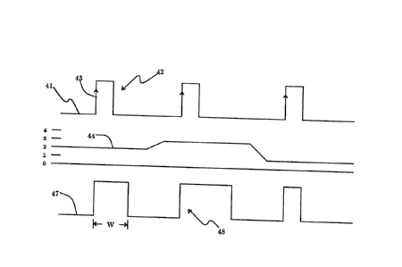
Figure ~ has three components. Typical input signal trace 41
comprises a serie~ of pulses 42, each having a leading edge 43. I~put weight
~ignal trace 44 varie~ in magnitude. The resultallt output of the PWM is out-
put signal trace 47 consisting of pulses, denoted generally a3 48. Note that
1312383
-2~
each output pul~e i~ triggered by the input pulse leading edge, and that the
width W of each output pulse i~ proportional to the value of the weight signal
input value. Other mechanisms with similar characteri~tics are Yiable.
A typical circuit ~or a PWM can be described as ~ollows: the input
5 ~piked ~ignal trigge~ a ~ip-~lop; an asynchronou~ feed-back loop resets the
~ip-flop; there is a time-delay in the output; this delay i8 determined by the
voltage on a leakage transi~tor; the higher the voltage, the faster the cirsuit
reset~. Other methods of implementing this circuit will be obvious to those
skilled in the art.
It is desired that on the backward~ ~ow of information that the sum-
mation be essentially linear, to remain within the bounds proscribed by Back
Propagation. However, on the backwards ~ow of error information, a PWM
can nonetheles~ still be u~ed. Since colli8ions will occur, what is desired i~ to
reduce the number of collision~, until they are negligable (and the system
15 respollds in a nearly linear manner~.
Experimentally, it has been seen that the values of ~ae~+ range from O
to 10, in medium sized networks. They rarely will go over 10. 1~ the number
of re~ultant spikes is divided by a factor of ten in the~e situations, the
exponential term becomes nearly linear (because 1--c~Z ~s ~, when z is small).
20 V.VI: Imptcmentin~ Forward Propa~at~on w~th Spike Trains
Figure~ Sa and 5b together depict an implementation of a Neural
Network, referenced herein as a Type O Neural Network. Figure 5a show~ a
matrix element, denoted generally as 59, and ~gure 5b depicts a processing
element, denoted gene~ally as SO. It is important to note that if these ele-
25 ments 59 alld 50 are sonnected in a matrix configuration, such as exampled inFigure 2, with type O matrix elements 5~ in matrix element locations 10's~
and with type O processing elements 50 in processing elements 20's locations,
the forward data propagation function can be performed.
Also with reference to Figure 2 it should be noted that hereinafter an
30 element that ser~es the function of one of the horizontal transmission line
pairs (e.g. 11a' and 12a', 11b' and 12b', 11c' and 12e', and 11d' and 12d')
may be refered to as a horizontal combining element. The horizontal combin-
ing elernent~ may be further di~tinquished as an input horizontal combining
element, i.e. one connected to an input processing elment, or as a hidden hor-
35 izontal combining element, i.e., one colmected to a hidden processing element.
~3~23~3
-27-
Also, a~n element that 3erve3 the ~nction of one of the vertical transmi3iion
line paris (e.g. 13c' and 1~c', 13d' and 14d', 13e' and 14e', or 13f' and 14f'),may be refered to as a vertical combining element. Matrix element3 that
directly couple with an input proces3ing element may be refered to a~ l'input1'
matrix elements (e.g. in Figure 2, matrix elementY 10a' through 10h').
Matrix element~ not directly couyples to an input proceYsing ele~nent may be
refered to a~ "hidden" matrix elements (e.g. in Figure ~, matrix elements
10i' through 10m').
Line 51 on both i~gures 5a a~d 5b conveys the output of a proce~sing
element to all the matrix elements to which it i8 connected. Line 52 on both
iEigures 5a aIld 5b serves as the combining unit while simulta~eously convey-
ing the output of the combining unit to proce3sing element above. Line 53 on
flgure Ba connects weight value 54 (which may be thought of as a fixed
weight value for this explanation) to the Pulse Width Modulator 55. The
other input to the Pulse Width Modulator i8 taken from Line 51, a~d the out-
put of the Pulse Width Modulator i3 OR'ed by element 7 onto Line 2. Line
52 terminate~ in ~gure 5b at time averaging element 57. Time averaging
element 57 average3 the input from line 52 over time, and provide~ an output
which repre~ents that average. Voltage to Frequency Element 58 produce~ an
output frequency which i8 dependent upon the input value. Line 51 ori-
ginates at the output of element 58.
It i8 imps)rtant to note that i~gure 5b repre~ent3 a hidden proce3sing
- element and that the input and output proces3ing elements may vary from
the repre3entation to accomodate the desired input or output vector. For
example, if the input vector iB a voltage, then time averaging element 57 is
not needed in the input processing element; and, if a ~roltage output i~
desired, then vs)ltage to frequency element 58 may not be needed in an output
processing element.
V.VII: A Method of Implementing ~he l)erivative of the Squa~h Function
One of the major requirements of the Back Propagation Algorithm is
the bacl~wards ilow of error. In the backwards f~ow of error, there is a lineal
sllmmation of the backward3 flowing error and a multiplication of it by the
net input (number of spi~es) run through the derivative of the squash func-
tion, ie.:
1 3 t 2383
-2~-
backwards erro~ x squash'( numbcr of sp~kes ) (71)
By examinillg the total of all the times between the pulse~, one can
find an interesting space. If we ignore inhibitory ~pike for the moment, the
5 amount of this time corre~ponds to:
OffTsmc--1--On7:ime (72)
AB it has been shown in equation 51
OnTime = 1--e -numhcr of spil~eo (73)
or
OffTirne = c--nt~mb~ f ~p~
Thi~ i~ exactly the derivative of the squash function (from equation 4~).
Therefore, if the error i~ propagated backwards when no spikes a~e present (or
equivalently, only c~amined when there are no spikes present), the time a~er-
aged multiplication i~ exactly a multiplication of the error by the deriYative of
15 the squash functio~ with respect to the net input -- precssel~ what is desired!
EIaving two parameters in the squash ~unction (as was derived in equa-
tion O) pose~ a problem for the back propagation algorithm, as the activation
function is now a function of two variables, rather than the single one before.
This can be accounted for by taking the partial derivathre3 of the activation
20 function first with one variable and then with another.
aQ (nctl+ t )
anet+
an~t~ = e ~(r~t +n~t ) _ e -net- (76)
Thi~ mean~ that the squash function and its derivatives (of Back Pro-
pagation) can be stated as:
J(net+,net~) = e~n~t (l- e~ t~) (77)
f ~ (net +, net~) = e~(nct +Aet~) (78)
f ' ( t+ t-) =--e~n~t (1--e~nctt) = _f(net+,net~)
It is necessary to examine the time intervals that we have ready access
to, to detirmine if there exists any time interval which is equivalent to the
30 pa~tial derivative of the s~uash function with respect to one or the other of its
13~23~3
-2
parameters.
The time when either type of ~pike (eith~r excitatory or inhibitory) i~
present i8:
t3me (anll sptk~ p~esent) = 1--e-(~t +n2t ) (80)
5 (Equation (80) can be quickly derived u0ing the identical method3 used in
previous sections.) The time when no spikes are present ii calculated as:
tim~(no sp~ke present) = 1-time(an~ sptke prcs~nt) = e~(n't +n~t ) (81)
This means that the partial deriYative of the activation function with
respect to the excitatory inputs i~ the equal to the time when no spikes, exci-
10 tatory or inhibitory, a~e present. To do backwards propagation of error forweights connected to ~ccitatory synapses one can u~e the time-multiplication
of the error with time when no spikes are present.
Gi~en ~rom equati~n 7~ that
aQ_ _~ (82)
anet~
15 we can see that $o for the backwards propagation of the error via weights con-
nected to inhibitory synapses, one can use the time multiplication of the error
with the time when ~loutput~ 8pike8 are present (as long as the sign o~ the
weight change i8 changed accordingly). This means that, by using the
methods of the pre~e~t invention, the computation of both the forwa~d ~quash
20 function and the derivatives of it are trivially computed with simple logical gates.
V.~II: Uultiplication by AN17'in~ ~wo Pulse Tra~ns
Another component of Back Propagal;ion i8 the manner in which the
weights are updated. This is (e3sentially):
_ = OutputR~lou, x E~rrorAjOu~ (83)
If the error in a node above is represented in a spike method, the calcu-
lation for the change of the weights is simple. It is (essentially) the logical
AND of the forward flowing spiked data signal and the spiked error signal.
If all signals in the network are represented as spikes, much of the
30 noi3e problem3 associated with pure analog signals is alleviated.
1 3 1 2383
-3
Fi~e ~S illustrates the logical AND of two spike train~. Signal trace~
~1 and ~2 depict typical input signals. Signal trace 63 i~ the logical AND of
the two input signals Bl and 62. Under the right circum~tances, the logical
AND of two spiked signal~ is equivalent to the multiplication of the two sig-
5 nals.
To show this, assume that each line i=1,2 has a probability P, that iti~ a one. Since the logical AND of two lines is one only when both input lines
are one, from simple statistics, the probability that a~ output line is one is
Pl xP2. It i~ clear to see that an input line will have a probability of being
10 one in proportion to the frequency on the line if the width of the pulse
remains constant. This i~ the method used in the circuits derived herein. The
output therefore will have a probability of being a one which is proportional
to the multiplication of the probabilities of the two input line~.
Hence, to multiply the Data and Error signals, when the spike model is
15 used, all that is required is a trivial AND gate. By averaging the output of
the AND gate o~er time, a true multiplication is performed.
V.IX: Rederivation of Back Propa~ation
Prior art Back Propagation Bum8 the excitatory and inhibitory (posi-
tive and negative) weights together, and there is only a single NetData which
20 drives the squash function. The Spike Model of this invention ~eperates the
excitatory and inhibitory weights into two catagorie~7 and since it has a tw~
parameter squash function, it is nece~ary to rederive a few equations of the
traditional Back Propagation utili~ing the new function.
The basic rule for modifying weights remains the same as in traditional
25 Back Propagation:
dwj, aE
dt awff
For brevity, let ~p;--aaE Since weights ca~ now be thought of as either
excitatory or inhibitory, equation 84 can be r~written by denoting an excit~-
tory weight as w+ and an inhibitory weight as wj,:
-31- 13t~3
dWj+i ~E
dt awii (85)
aE aOpj anetpj+ (86)
aOpi an~tpj+ awj+j
= ~pj f +(netpj~,nztpj ) pi (87)
dw~i aE
dt aw,i (88)
aE aOpj anetpj- ~89)
aOpj anetpj~ aWj-i
= ~pj f (n~tpj+,netp; ) op, (~0)
The update of the excitatory and inhibitory weights a~e identical,
except for which pa~tial derivati~,re of the squa~h function f is in the node
above. Both u~e the same net error (yp;). Both use the same data from $he
lower node (pi)-
The computation of the net error (~pj) in hidden node~ is altered. The
rederivation is a3 follow~:
-- aa~
~: 15 2 a~ ~Op~ antp,+ ~ a}~ aOp~ ~anetp~ 2)
~:~ j+ aOpj an~tpj+ aOpj j aOpj anetpj- aOpj
pj f t+(n~tpj ~netpj ) wti + ~ ^JPj f t (r~etpj~,netp; ) w~j~g3)
The above deri~atiQns are ~ufficient to demonstrate the feasibility of
the other derivations in this disclosure.
::
V.X: BackPropa~tion Implement~t~on
The Spike Model Back Propagation Neural Network a~ developped and
disclosed herein iB readily implemented in hardware. There exist many
methods to create a hardware environment for this version of the algorithm.
Two exemplary circuits will be examined. A Type I Back Propagation Neural
1 3 1 238~
-32-
Network uses spikes trains for the forward data Iqow and an analog signal is
used for the backwards ~ow of error i~formation. These signals are multi-
plexed onto the same data line. The Type II Back Propagtion Neural Net-
work uses spike trains for both the forwards and backwards flow of informa-
5 tion.
The Back Propagation algorithm, when implemented in the SpikeModel specifies the following equations are to be per~ormed ;n what can be
called a no~lincar ~idirecti~na~ matrt~ multiplier:
F~awDataj = fl( ~ Data, x Wj, ) (94)
RawErrorj = f2( ~ Error; x w;, ) (95)
dtii = Errorj x Datai (96)
The functions fl and f2 are the intrinsic functions created by the
hardware instantiations. As was shown, fl (for the forward ~ow of data
information) can be made to perform the essential characteristics of the
15 squash function, by OR'ing the spike pulses together. On the other hand,
anything other than a linear J2 (for the backwards flow of error information),
will cause problems (or the nece~sity to create an inverse function).
Equations ~4 and ~5 detille two matrix multiplications. A vector of
data signals i8 multiplied by a weight matrix to provide a vector of net data
20 signals, whose elements are the~ individually "squashed" to create a new set
of data 8igIlal8. Similarly, a vector of error signals are multiplied by the same
- weight matrix (ater it ha~ been inverted3 to provide a vector of net error ~ig-
nals. If f2 is linear, then no squashing of thii net error vector takes place.
Equation ~6 defines how the weight is to be changed. The function~ associ-
25 ated with a single element in the matrix are grouped together and are collec-tively called a matrix element. Together, they form the non-linear bidirec-
tional matrix multiplier. This will become more clear as the hardware imple-
mentations are explained.
It still remains that there need3 to be a function which converts the
- 30 RawData and RawError values into the Data and Error values. One cannot
directly forward the informat;on, because the colliding spikes of the ~awData
signal will not be of a reasonable form. It is po~sible that the RawError si~nal
1 3 1 2383
-33-
can be passed directly, in some circuit designs (ie. if the paa~age of informa-
tion is linear enough and the format i~ correct for the lower layer~). However,
since the number of these elements which must be phy~ically instantiated is
much ~maller than the number of interconnections, it behooves the designer
5 to select the smallest design possible for the interconnections.
For simplicity when labelling wires in the hardware version, new names
will be given to the elements in the Back Propagation algorithm. The names
Data ~d Error indicate that the lines generally communicate the obvious
information. When applicable, the name Po3itive Error indicates that the
10 line transmits the positive portion of the Error signal. The negative portionof the Error signal i~ tran~mitted by the line Negative Error. To derive the
total error signal, some combination of the previous lines i8 nece~sary (such assummation).
lFigur~ 7 depicts a stereotypical trace 70, of a multiplexed data and
15 error signal having all upper half, denoted generally as 71 and a lower half,denoted generally as 72, seperated by midline 76. The data signal iB present
on the upper half of the trace. The magnitude of the date value is
represented by and equivalent to the duty cycle of the data pulses. The duty
~ycle is the time (width) W of a spike, divided by the total time (width)
20 between the start of two spikea Hence, the value of the duty cycle varies
between 0 and l. The error sigr3al i~ present on the lower half of the trace.
The magnitude of the error value is repre~ented by and equivalent to the
height H of the signal pulses from a refere~ce level, depicted by line 77. Note:if the signal pules goe~ below line 77 that the repre3ented error signal i8 nega-
25 tive.
V.XI: Tvpc I Back Propa~7ation Neural Net~ork
Figure~ 8~ and 8b depict a set of circuits which can perform BackPropagation utilizing the Spike Model of this invention. This implementation
ver~ion shall be called Type I. Figure 8a i8 a representative circuit for a
30 Type I matrix element, denoted generally as 80. Figure 8b is a representa-
tive circuit for a Type I processing element, denoted generally as 180. As in
the previous Type 0 model, these elements 80,180 can be arranged similar to
the configuration of Figure 2, with Type I matrix elements 80 in place of
matrix element~ 10, and Type I processing elements 180 in the place of Pr~
35 cessing Elements 20.
~ 3 1 23~3
-34-
Horizontal combining element line 81 i8 directly connected to one pro-
ce3iing element and one or more matrix elements 80. The forward flow of
data on line 81 is in the form of spikes with their frequenc~ being the value ofthe activation level of the connected processing element. The width of the
data spike~ is small and iF7 used to control the learn rate, the details and
implementation of which are not discuss,ed in this disclosure. During the off-
time of the data spikes, the net error value i8 propagated as an analog value
mea~ured from some reference value a~ i8 illustrated and deæAbed in refer-
ence to Figure 7.
Vertical combining element line 82 i8 connected to one or more matrix
elements and to only one proce sing element. Line 82 carriei a multiplexed
net data ~pike train signal ~orward and an analog error sigrlal backward8.
This error signal on line 82 is pre~ent during the o~-time of the data spike,
similar to that ~hown a8 trace 70 of Figure 7.
16 Because the data and error 3ignals are multiplexed on a single line in
the Type 1 Back Propagation Neural NetworL~, line 81 carries information
equivalent to the information carried on lines 11, 12 of Fi~ure 2 and line 82
carries information equivalerlt to the information ca~ried on lines 13, 14 of
Figur~ 2.
The Type I matrix element circuit of Figure 8a works as follow3. To
p3~18 the data information forward through type I matrix element 80 the
PWM element 83 has ~ inputs line 81 and the weight value output of
integrator 84. Whenever a data pul3e on line 81 transi3tions upwards, PWM
83 fire~ for a duratio~ dependent upon the value of the weight received from
integrator 84. The output of PWM 83 is "OR"'ed onto line 82, such as by
simply con~ectiDg it to the line.
It is important to note that the OR'ing of the s,piked output data infor-
mation o}lto liDe 82 by all OI the matrix elements comlected to that line
accomplishes the squash function as discu~ed previously in relation to equa-
tion 46.
To send th0 analog error signal received on line 82 backwards, error
averager 85 samples the error signal on line 82 and output~ an average of it.
Error averager 85, when no error signal is pre~ent on line 82 (ie. when an
OR'ed forward data pulse is present), assumes a value of zero error. By doing
so, the product of the error times the derivative of the squash function is per-formed. Multiplier 8~ receives the average error from error averager 85 and
131238~
-35-
the weight from integrator 84, and multiplies them, and outputs the product
via a summation onto line 81 through resistor 87. Resistor 87 is overpowered
when a data spike is present, such that the error value does not effect any
change on a data spike.
The matrix element 80 depicted in ~gure 8a is representatiYe of a hid-
den matrix element. Input matrix elements are those connected directly to an
input processing element, e.g. matrix elements 10a', 10b', 10c', 10d', 10e',
lOf', lOg' and 10h' of ~igure 2. Input matrix elements do not need means for
the back propagation of weighted error.
The following circuit produces the weight update signal. Voltage gate
88 has input D connected to line 82 and input G connected to the output of
AND gate 8~. Voltage gate 88 turn~ on when input G i3 high, i.e., it passes
the error voltage from D through to output O. AND gate 89 has one input
connected to line 81. Thi~ input ie high only duriTlg the on-time of forward
data spikes. Since the width of the forward data spikes corre~ponds to the
learn rate, the on-time of AND gate 8~ varies accordingly. The other input to
AND gate 8~ i8 inverted and is connected to line 82. Thus this line is high
when the error value (low) is on line 82. The re~ultant output of Voltage
Gate 88, is equivalent to ddt ~ which is the time-averaged equivalent of
learn_rat~ x f ' ( net_data) x erJ'r~bo~r x outpu~/OtO -
Integrator 84 receives as input the output O of Voltage Gate 88.
~tegrator 84 integrate~ thi~ signal over time. The output of integrator 84 i~
the weight value for matrix element 80.
The Type I processing element 180 depicted i~ i~gure 8b wor~s as fol-
lows. For the forward flow of data logical buf~er 181 receives from line 82 the
multiplexed Data a~d Error signals and strips out the error signal by turning
that time period into a true ~ero value. The output of logical buf~er 181 i~
time averaged, such as by capacitor 182. The time a~eraged signal is received
by Voltage to Frequency ~lement 183 which convert~ the time averaged signal
into a pulYe train, and pre~ents that as output on line 81.
For the backward~ flow of error information through Type I processing
element 180, voltage gate element 184 3amples the error signal available on
line 81 when no data signal is psesent by allowing the voltage present on line
81 through a~ output when line 81 is not high. Capacitor 185 time averages
this output signal. Analog buffer 18~ receives this time averaged error signal
1 3 1 2383
-3~
and provides it to resistor 187. Re~istor 187 i~ overpowered when a forward
data pulse is presented on line 82 by a matrix element. When no data pulse
is present on line 82, Resistor 187 provides a backward~ error signal on line 82to the matri~c element~ connected on line 82.
Proce~sing element 180 i~ representative of a hidden processing element
for a Type 1 Back Propagation neural network. The input and output Pro-
cessing Elements may vary somewhat depending on the desired from of the
input, output and error vector~. Particularly, the input proce3sing elements
could exclude the mean~ for the backward ~ow of error information.
The maJOr benifit of these circuit~ is that only one wire is needed for
communications (as opposed to two, one for data and one for error, as shown
in Fig~ 1 and 2). In VLSI architectures, where the the numher of pins (wires
going on and off of a chip) on a ~ingle Chip i8 critical, thi~ can be ve~y
benificial. The main detraction i~ that this circuit is susceptible to noise in
the one area in which noise i8 extremely harmful, i.e., in the analog error 8ig-nal which must be kept relatively small compared to the total range of vol-
tages 80 that it ca~ always be distingui~hed from the data signal. Thu3, there
i3 little margin for noi3e immunity.
V.XII: T~pe II Back Propa~ation Neural ~twork
Figures ~a a~d S~b together depict the Type II Back Propagation
Neural Network circuit which u3es spike trains for both for the fo~ward ~ow of
data information and the backwards ~low of error information. Figure ~a is
a block diagram of an e~emplary Type II hidden matrix element, denoted
generally a~ igure ~b i8 a block diagram of an exemplary Type II hid-
den proce~ing element, denoted generally as 90. A~ with the previously di~-
cussed Type 0 and Type 1 matrix elements and processing elements, the Type
II element~ can be ~ranged ~imilar to the arra~gement of Figure 2 (or
expanded) to form a neural network. Proce~sing element 90 and matrix ele-
ment 1~0 are representative of Type II hidden elements. Type II input and
output elements will vary in obvious manner~ from the hidden elements
described.
As before, the component~ of element~, particularly at the input and
output levels will vary according to the de~ired input, output and error vec-
tors. Line~ 92, ~4 and 96 connect one processing element below to one or
more matrix elements above it. Lines ~1, 93 and 95 connect one processing
1 3 t 2383
-37-
element above to one or more matrix elements that provide data to that pr~
cessing element.
The spikes utilized in this circuit are not signed (ie. the are positive
going only). Two lines are used for backwards propagation of error signals.
5 One is used for positive errs~r, and the other i8 used for negative error signals.
The Matrix Element Type II produces two raw pul~ed error signals, one a
positive 3nd the other a neg~ive. The Processing Element converts these sig-
nals into Positive Pulsed Error and Negative Pulsed Error signals.
In flgure S~a, the forward flow of data information through matrix ele-
10 ment type II 1~0 i~ identical to that in Matrix Element Type I. Pulsed dataon pulsed data line 9~ i~ received by PWM element 103a which also receives a
weight value from integrator element 102. The output of PWM element 103a
i8 OR'ed onto raw pulsed data line 91 by psued~element 104a a~ a portion of
the raw squashed data signal.
However, the backwards ~ow of error information is ~implified, because
instead of multiplexing both error signs on a single line, they are significa~tly
separated. Ideally, whenever the error i8 positive, the error is fed down Posi-
tive Pulsed Error line S3, and correspondingly, a negative error is fed down
Negative Pulsed Error line 95. 1~ some implementations, lower layer3 of the
network may have both positive and negative errors present, becau~e the error
signals are not ca~lcelled. When thi~ happens, a simple cancellation circuit
can be used to disce~ the difference and leave only one signal with active
information.
For the backwards propagation of error information through matrix
element type 11, the pulsed error has a po~itive portion on Positive Pulsed
Error line ~3 and a negative portion on Negative Pulsed Error line 95. PWM
elements 103b and 103c receive input from lines 93 and 95 respectively.
PWM elements 103b and 103c both receive as weight input the weight output
value from integrator element 102. Outputs from PWM element~ 103b and
103c are wire-OR'ed onto Positive Raw Pulsed Error line g4 ~d Negative
Raw Pulsed Error line 92 by psued~elements 104b and 104c respectively.
The weight value generated by integrator element 102 is updated by its
two input signals: a positive update signal generated by AND element 101a,
and a negative update signal generated by AND element 101b. The inputs of
AND element 101a are pulsed data line 96 and positi~re pulsed error line 93.
The nputs of AND element 101b are the pulsed data line 96, and negative
.
.
-38- l 3 1 2383
pulsed error line ~5. Integrator mean~, such as integrator element 102, tal;es
its positive and negative inputs, calculates the differense between them and
provides a3 weight output the integration over time of that calculated
difference.
Fi~ ure S~b depicts a Type II Prccessing Element, denoted generally as
~0. For the forward flow of data in~ormation through proce~sing element ~0,
time averaging element 97a receives the squashed data from raw pulsed data
line 91. and provides a~ output the average value of that signal ~ver time. A
time averaging element may be as simple as a~ ordinary capacitor, but may
include a logical buffer, to clean the signal8 up into desired discrete boolean
values. Voltage to Frequency element 98a recieves the output of time averag-
ing element 97a and provides output to pulsed data line ~ as a pulsed data
signal at a fiequency line~rly proporl;ional to the output of time averageing
element 97a.
For the backwards ~ow of error illformation through processing ele-
ment 90, AND elements ~gb and 99c receive the error in~ormation from posi-
tive raw pulsed error line 94 and Negative Raw Pulsed Error line 92, respec-
tively. Also, AND elements 99b and 99c recevie the complement of the for-
ward fiowing 3quashed data from Raw Pulsed Data line 91. This has the
effect of tim~multiply'ing the feedback error by the derivative of the squa~h
function. The outputs of AND elements 9~b a~d 9~c are fed into time
averaging elements ~7b and ~7c respectively. The outputs of time averaging
element~ 97b and ~7c are fed into the input~ of Voltage to Frequency ele-
ments ~8b and ~8c re pectively. The output~ of Voltage to Frequency ele-
ments ~8b and 98c are fed onto po3itive pul~ed error line 93 aIld negative
pulsed er~or li~e 95, respectively, as pulsed data output signals.
An of~8et problem may occur if the width~ of the Positive a~nd the
Negative Pulsed Error lines are not identical. 1~ one is longer than the other,
there will be an offset towards that direction. This may or may not be a
significant problem under various circumstance~.
l@igure 0c depicts an expansion of a Type II Processing Element,
denoted generally as 90c. Processing element 90c is for use in a modified
Type II back propagation neural network, in which weights values may be
effectively both positive and negative. The matrix elements in this system
may be thought of as a pair OI matrix elements one inhibitory, one excitatory.
An excitatory matrix element would be similar to matrix element 190, and
~ 3 t 2~3
-3~
would be connected to lines 91, 93 and 95, and would output a excitatory raw
pulsed data output ~ignal onto line 91. An inhibitory matrix element is
modified ~uch that element 104b i3 connected to line 92 and element 104c i8
connected to line 94. This would then send the error back with the opposite
sign, as is necessary. An inhibitory matrix element would be connected to
lines 91', 93' and 95', and output an inhibitory raw pul~ed data output signal
onto line 91'.
For the forward flow of data information through processing element
90c, AND element lû~ rec0ive~ the excitatory squashed data from Excitatory
Raw Pulsed Data line ~1 and the complement of the inhibitory squashed data
from Inhibitory Raw Pulsed Data from line 91', and AND's the two signals
together, providing the results on line 108. Time averaging element 97a
receives this AND'ed signal from line 108 and provides as output the average
of that signal over time. Voltage to Frequency element 9$a recieves the out-
put of time averaging element ~7a and provide~ output to Pulsed Data line
96.
For the bac~wards flow of error information through processing ele-
ment 90c, to the excitatory inputs, AND elements 99b and 99c receive the
error information from Positive Raw Pulsed Error line 94 and Negative Raw
Pul~ed Error line g2, re~pectively. OR gate 105 receives a8 input the excita-
tory ~quashed data from E~ccitatory Raw Pulsed I~ata line 91 and the inhibi-
tory squP~hed data from l~hibitory Raw Pulsed Data from line 91'. OR gate
105 produces an OR'ed signal on line 107. AND elements 99b and 99c further
receiYe the complement of the OR'ed sinal on line 107. This ha3 the effect of
time-multiply'ing the feedback error by the derivative of the squash function
with resp0ct to the excitatory raw squashed data. The outputs of AND ele-
ments 99b and ~c are fed into time averaging elements 97b and 97c respec-
tively. The outputs of time averaging elements 97b and 97c are fed into the
inputs of Voltage to Frequency element~ 9~b and 98c respectively. The out-
puts of Voltage to Frequency element~ 98b and 98c are fed onto Positive
Pulsed Error line 93 and Negative Pulsed Error line 05, respectively.
For the backwards ~low of error information through processing ele-
ment 90c, to the inhibitory inputs, AND elements 99b' and 99c' receive the
error information from Positive Raw Pulsed Error line 94 and Negative Raw
Pulsed Error line 92, re3pectively. Also, AND elements 99b' and 99c' receive
the complement of the AND'ed signal from line 107. This has the effect of
1312383
-4~
time-multiply'ing the feedback error by the derivative of the squash function
with respect to the inhibitory raw squa3hed data. The outputs of AND ele-
ments 99b' and 99c' are fed into time averaging elements 97b' and 97c'
respectively. The outputs of time averaging elements 97b' and 97c' are fed
5 into the inputs of Voltage to Frequency elements 98b' aDd ~c' respectively.
The outputs of Voltage to Frequency elements 98b' and 98c' are fed onto
Positi~e Pul~ed 13rror line 93' and Negative Pulsed Error line ~5', respectively.
V.~I: WhV This Is Bettcr
From the foregoing description, it is seen that the spike system of Baclc
10 Propagation of the present invention avoids the ma~ior problem of offset errors
inherent in a straight analog system.
~ a tim~multiplication, as i~ used in thia invention, the offset is lim-
ited by the resolution of the time-value~, rather tha~ by the matching of com-
ponents. This resolution of the time v~lue~, rather than adding a constant
15 offset, is like multiplying in a con~tant; this is not bad in the back propaga-
tion algorithm, lS it primarily a~ect~ the learn-rate, which has been shown to
be allowed to be variable by weight.
Other ma~ior benefit~ of the spike system include a dramatic reduction
in the number of component~ necessary to implement the system; no four-
20 quadrant multipliers are neces~ary; no active elements which perform squashor squash-prime fu~ctions; and offset noises are not present.
Although the invention has been shown a~d described with reference to
cetain spec;fic embodiments, it is to be under~tood that this matter is to be
interpreted as illu~trative and not in any limiting sense, and that many
25 modifications and substitutions will become apparent to those skilled in the
art. For example, it should be readily apparent that optical systems will be
greatly enhanced through the use of these multiplicative mechanisms, as there
exist~ no way, currently, to produce the analog multiplication of two light sig-nals, but the OR'ing of two light ~ignals is readily feasible. Also, it is possible
30 to modify the Type II circuitry to have a single backwards error spike pulse,a~d another line represent the sign, or to use a positiYe going spikes and nega-tive going spike on the same line, etc. This disclosure is intended to cover in
the appended claims such modifications and changes a~ come within the true
spirit and scope of the invention.
~ 3 1 2383
-41-
What I claim i~: