Note: Descriptions are shown in the official language in which they were submitted.
~3~2~
1 TITLE OF THE INVENTION
Microprobe, Pre~aration thereof and Electronic Device
by use of said Microprobe
5 Background of the Invention
-
Field of the Invention
This invention relates to a microprobe having
an extremely small radius of curvature at the tip end
portion which is used for a probe for measurement of
10 muscle activity current, a probe for STM (Scanning
'runneling Microscope), a probe for high density
recording-reproduction device or a probe utilized for
an encoder which performs positional information
measurement in micropositional determination,
15 dimensional measurement, distance measurement, speed
measurement, etc.
Related Background Art
In recent years, the recording capacity of
data in recording-reproduction device i5 becoming
20 increasingly greater year by year, and the size of
recording unit is becoming smaller, while the
recording density higher. For example, in digital
audio disc, the size of the recording unit has become
even about 1 ~m . There is active development of
25 memory materials in its background, and inexpensive
and high density recording medium by use o~ an organic
,
~ ~ i
~2~
~3
-- 2 --
1 thin film of an organic dye, a photopolymer, etc. is
now appearin~ on the marke~.
On the other hand, Scanning Tunneling
Microscope (hereinafter abbreviated as STM) capable of
5 observing directly the electron structure of the
surface atcms of a conductor has been developed [G.
Binnig et al r Helvetica Physica Ac~a. 55, 726 (1982)]
and it has become possible to measure real space ima~e
with high resolution regardless of whether it is
1~ single crystal or amorphous, and there i5 also the
advantage that observation is possible at low power
without giving damage to the medium. Further, it can
be also used for various materials through actuation
in the atmospheric environment, and therefore a broad
15 scope of applications are expected therefor.
STM utilizes the phenomenon that tunnel
current will flow when a probe of a metal (probe
clectrode) and an electroconductive substance are
brought near to a distance of about 1 nm under
20 application of a voltage therebetween. The current is
very sensitive to the distance change between the
both, and by scanning the probe so that the current or
the average distance between the both may be
maintained constant, a surface information of the real
25 space can be obtained. In this case, the resolving
power in the plane direction is about 1 A.
,' .
~ 3 ~
1 By applying the principle af STM, it is
possible to perform high density recording and
reproduction sufficiently on the atomic level (several
A). As the method for recording and reproduction in
5 this case, it has been proposed to perform recording
by changing the surface state of an appropriate
recording layer by use of a particle ray (electron
beam, ion beam) or a high energy electromagnetic wave
such as X-ray and an energy ray such as a visible ray,
10 a UV-ray, etc. and effect reproduction by STM, or to
perform recording and reproduction by means of STM by
use of a thin film layer of a material having the
memory effect for the switching characteristic of
voltage and current as the recording layer, for
15 example, ~-electron-system organic compound or a
chalcogenide as the recording layer.
For performing recording and reproduction on
the molecular level, the recording density becomes
higher as the curvature of radius of the probe tip end
20 opposed to the recording layer i5 smaller. Therefore
a probe is desired ideally which has a sharpness of as
sn~all a~ about an atom level.
For measuring the muscle activity current of a
human body, since a single cell of a human body has a
2~ small size of about 2 ~m, the radius of curvature of
the tip portion of microprobe is required to be
~, :
: - ~
.
13~2~ ~
1 smallest.
Further, an encoder is constituted of a
standard scale having the informa~ion concerning
position or angle and a detecting means for detecting
5 the information concerning position or angle by moving
relatively thereto. The encoders are classified into
several types depending on the standard scale and the
detecting means, such as the optical encoder, the
magnetic encoder, the capacitance encoder, etc.
As the encoder having resolving power of
atomic level, there is the parallel movement detecting
device disclosed in Japanese Laid-open Patent
Publication No. 62-209302 applying the basic
principle of Scanning Tunneling Microscope disclosed
15 in U.S. Patnet 4343~g3 which is capable of observing
the information of a sample surface with atomic-level
resolving power as already known.
In the prior art, such an encoder is provided
with a standard scale concerning length and a probe
20 provided in proximity to the sca1e, and has the
function of encoding by signal processing of the
information from the tunnel current flowing between
the standard scale provided with a driving mechanism
and a probe as the signal source.
The`probe for detecting the tunnel current of
the above encoder is required to have a small radius
1 3 1 2 9
1 of curvature at the tip end in order to provide a high
performanc~ and high resolution encoder.
In the prior art r the probe having such tip
with small radius of curvature has been prepared by
5 use of mechanical polishing and electrolytic
polishing. According to the mechanical polishing
methodr it is possible ~o prepare a probe having a
fine tip portion with a radius of curvature of 5 to 10
~m by cutting and polishing a wire of fibrous crystal
10 (Pt, etc.) by means of a clock lathe. According to
the electrolytic polishing method, a wire of 1 mm in
dia~eter or less (W, etc.) is held vertical in the
axis direction, dipped in an electrolyte to about 1 to
2 m~, and the wire is subJected to electrolytic
15 polishing by application of a voltage between the wire
and the opposed electrode in the electrolyte, whereby
a probe having a fine tip of about 0.1 to 1 ~m of
radius of curvature can be prepared.
However, of the preparation methods of
20 ~icroporbe of the prior art as described above, the
cutting method has the drawback that the probe will be
soon bent because stress is applied on the probe,
while the electrolytic polishing method, although
finer probe as compared with the cutting method can be
25 preparedr has the drawback that it is extremely
difficult to prepare a fine probe with a radius of
. , .~ .
~, , - . :
- : , . : . .
. . . .,
.
.' ' , ~ ~' '' :
. , .
~3~2~
1 curvature on the order of atomic or molecular level.
It is also di~ficult according to the method
for preparing microprobe of the prior art to prepare a
microprobe of which the radius of curvature at the tip
5 is on atomic or molecular level with high
reproducibility.
The probe electrode prepared according to the
above method, because it is fixed on a device by
holding by fixing with a screw or by spring force, is
10 weak in rigidity so far as the tip of the probe
electrode is concerned, namely having the drawback of
law natural frequency.
By use of the probe prepared by the method of
the prior art, because the tunnel current draw-out
15 electrode is apart from the detecting portion, it is
susceptible to acoustic vibration, floor vibration,
electric noise, whereby the amount of the information
detected by the probe is decreased.
Further, for example, in the high density
~ recordin~-reproduction device as mentioned above,
~ince recording or reproduction of data is pe~formed
by scanning the XY stage while moving one probe, the
movement distance of the probe becomes longer, whereby
there is involved the drawback that the recording and
25 reproduction speed becomes slow.
Thus, it has been desired to have a probe
~L 3 ~
1 having a small radius of curvature of the tip.
SUMMARY OF THE INVENTION
The present invention has enabled performing
5 recording and reproduction at high density and with
high reliability or po~itional determination and
measurement of length at high precision by use of a
single cry~tal for the probe electrode.
More specifically, the present invention
10 provides an electronic device by use of a probe
electrode comprising a single crystal for recording
and reproduction or an electronic device comprisiny an
encoder by use of a probe electrode comprising a
single crystal for positional determination and
15 measurement of length, etc.
According to an aspect of the present
invention, there is provided a microprobe, comprising
a single crystal provided on a part of one main
surface of a substrate or a part of a thin film formed
20 on one main surface of the substrate.
According to another aspect of the present
invention~ there is provided a microprobe constituted
o~ a single crystal having an apex portion surrounded
by facets having a specific plane direction and
25 comprising à specific crystal face.
According to still another aspect of the
' ' : ' ~ ... . ~ ;
~ .
.
~ 3 ~
1 present invention, there is provided a ~ethod for
preparing a microprobe, comprising the step of
providing on a part of one main surface of a substrate
or on a part of a thin fil~ formed on one main surface
5 of the substrate a different material having
nucleation density sufficiently larger than the
nucleation density of said substrate or thin film, and
being small to such an extent that only a single
nucleus can be grown thereon, and the step of forming
10 a single crystal by growing a single nucleus on said
n~aterial.
According to a further aspect of the present
invention, there i5 provided a method for preparing a
microprober comprising the step of la~inating on a
15 single crystal substrate an insulating layer having an
opening so that a part of said single crystal
sub~trate may be exposed, and the step of growing a
single crystal having an apex portion surrounded by
facets having a specific plane direction and
20 comprising a specific crystal face by selective
epitaxial growth from said opening.
According to a still further aspect of the
present invention, there is provided an electronic
device for performing recording and reproduction,
26 having a probe electrode comprising a single crystal,
a recording medium provided in opposition to said
., .
~ 2 ~ 3 .~,
1 probe electrode and a means for applying voltage
between said probe electrode and said recording
medium.
According to a still ~urther aspect of the
5 present invention, there is provided an electronic
device, comprising an electroconductive standard scale
which becomes the standard with respect to length, an
electroconductive probe constituted of a single
crystal with its tip being arranged in proximity to
10 said standard scale face, a means for applying voltage
between said standar~ scale and said probe, a means
for detecting the tunnel current value flowing between
said standard scale and said probe and outputting the
signal corrresponding to the relative movement amount
15 in the lateral direction between said standard scale
and said probe based on said tunnel current value, a
means for detecting the relative movement amount and
the relative movement direction in the lateral
direction between said standard scale and said probe
20 based on the outputting signal from said signal
outputting means t and a means for counting the
relative deviation amount in the lateral direction
between said standard scale and said probe from the
signals of said relative movement amount in the
25 lateral direction and said relative movement
direction.
.
'' ' '~ '
. ~ -~. .. .
~L 3 ~ r
-- 10 --
1 BRIEF DESCRIPTION OF THE DRAWINGS
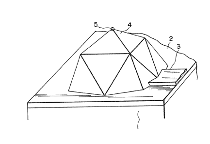
Fig. 1 is an appearance view of an embodiment
of the present invention;
Fi~. 2 is a sectional view of another
5 embodiment of the present invention;
Fig. 3 is a plan view of the embodiment in
which the present invention is applied for a current
detecting probe;
Fig. 4 and Fig. 5 are respectively sectional
10 views showing the preparation steps cut along the
lines A-A and B-B in Fig. 3;
Fig. 6 is a plan view of another embodiment in
which the present invention is applied fo~ a current
detecting probe;
15Fig. 7 and Fig. 8 are respectively sectional
views showing the preparation steps cut along the
lines A-A and B-B in Fi~. 6;
Fig. 9 and Fig. 10 are plan views of the
embodiment in which the present invention is applied
20 for a current detecting multi-probe;
Fig. 11 is a sectional view of anoth~r
embodiment of the microprobe of the present invention;
Fig. 12 is a sectional view of still another
embodiment of the microprobe of the present invention;
25Fig. 13 is ~ drawing for Illustration of the
.
. ~ .
~L3~2~ ~
-- 1 1 --
1 principle of the crystal formation treatment;
Fig. 14 and Fig. 15 are respectively sectional
views of other preparation steps cut along the lines A-
A and B-B in Fig. 3;
Fig. 16 is a perspective view of the external
form by the facet of the Si single crystal having the
plane direction of (100);
Fig. 1~ is a schematic diagram of the
recording-reproducing device by use of the microprobe
10 of the present inven~ion,
Fig. 18 is a black diagram showing an example
of the high density recording-reproducing device by
use of the micro-multi-probe of the present invention;
Fig. 1~ and Fig. 20 are respectively
lS characteristic charts showing the voltage-current
characteristics of the recording medium 184 in Fig. 17
and Fig. 18;
Fig. 21 is a block diagram showing
illustratively the recording-reproducing device;
Fig. 22 is a principle diagram showing the
positional relationship between the coordinate axis of
the present invention and the recording position;
Fig. 23A i9 a plan view showing one mode of
the recording medium of the present invention;
Fig; 23B is a A-A' sectional view thereof;
Fig. 24 is a schematic diagram showing one
'
-', ,, . . . -
1 3 1 2 ~
- 12 -
1 mode of the positional relationship between the
coordinate axis and the recording position on the
recording medium surface of the present invention;
Fig. 25A is a plan view of the recording
5 medium of the present invention, Fig. 25B is a A-A'
sectional view thereof;
Fig. 26 is a schematic diagram showing the
recording position on the recording material surface;
Fig. 27A is a plan view of another recording
10 medium used in the present invention;
Fig~ 27B a A-A' sectional view thereof;
Fig. 28 is a constitutional diagram of the
encoder by tunnel current detection according to an
embodiment of the present invention;
Fig. 2q and Fig. 30 are waveforms showing the
signals obtained in the respective constituent parts
in Fig. 28.
DETAILED DESCRIPTION OF T~E PREFERRED_EMBODIMENTS
The microprobe of the present invention is
formed of a single crystal.
The present invention has a specific feature
in a microprobe constituted of a single crystal having
an apex portion surrounded by facets having specific
2~ plane directions and comprising specific crystal
~aces.
2 ~ ~ ~
1 More specifically, there is provided a method
for preparin~ a microprobe, comprising a step of
providing on one main surface of a substrate or on a
desired part of a thin film formed on one main surface
5 of said substrate another kind of material having
sufficiently larger nucleation density than said
substrate or thin film and being sufficiently small to
the extent that only a single nucleus can be grown
thereon, and a step of forming single crystal by
10 growing a single nucleus on said material.
There is also provided a method for preparing
a microprobe of a single crystal, having a step of
laminating on a single crystal substrate an insulating
layer having an opening so that a part of said single
15 crystal substrate may be exposed, and a step of
subjecting a single crystal having an apex portion
surrounded by facets having ~pecific plane directions
and comprising specific crystal faces to selectiv~
epitaxial growth from said opening.
Further, the present invention provides an
electronic device for performing recording and
reproductionr having a probe electrode comprising a
~in~le crystal, a recording medium provided as opposed
to said probe and a means for applying voltage between
2S said probe èlectrode and said recording medium.
Also, the present inventlon provides an
,
1 3 ~
- 14 -
1 electronic device utilizing an encoder, having an
electroconductive standard scale which becomes the
standard with respect to length, an electxoconductive
probe constituted of a single crystal with its tip
5 being placed in proximity to said standard scale ~ace,
a means for applying voltage between said standard
scale and said probe, a means for detecting the tunnel
current value flowing between said standard scale and
said probe and outputting the signal corresponding to
10 the relative movement amount in the lateral direction
between said standard scale and said probe based on
said tunnel current value, a means for detecting the
relative movement amount and the relative movement
direction in the lateral direction between said
15 standard scale and said probe based on the outputting
signal from said signal outputting means, and a means
for counting the relative deviation amount in the
lateral direction between said standard scale and said
probe from the signals of said relative movement
20 amount in the lateral direction and said relative
movement direction.
In the following, embodiments of the present
invention are to be described.
First, an example of microprobe appearance of
25 the present`invention is shown in Fig. 1. It e~hibits
an appearance provided with a single crystal probe
` ~ 3~ 2~ ~
- 15 -
1 having a thin film (insulating film) 2, an electrode 3
on a substrate 1 and an information reading portion 5
at the tip.
Fig. 2 is a side view of the embodiment in
5 which the single crystal probe 4 formed according to
the present invention is provided in a plural number.
Another embodiment of the present invention
using the microprobe as the current detecting probe is
shown in a plan view in Fig. 3.
In this embodiment, a single crystal probe 4
having an apex portion surrounded by specific facets
is provided on a substrate (not shown in Fig. 3). In
the vicinity of the single crystal probe 4, a source
electrode 32, a gate electrode 31, a drain electrode
15 33 and a thin film resistance 35 are provided. These
constitute a MOS transistor 34 for amplifying the
probe current. The probe current detected by the
probe 4 is on the order of 10 A, but a probe current
on the order of 10 7A can be obtained by amplification
20 with the MOS transistor ~4. Also, since the probe
current detected by the single crystal probe ~ is
i~mediately amplified without being led out externally
of the substrate, the S/N ratio can be improved by far
greater a~ compared with the case where the probe
25 current i9 àmplified after led out of the substrate.
Next, the method for preparing the current
-` ~ 3 ~
- 16 -
1 detecting probe in Fig. 3 is to be described.
Fig. 4 is a sectional view showing the first
preparation step cut along the line A-A in Fig. 3.
Fig. 5 is a sectional view showing the first
5 preparation step cut along the line B-B in Fig. 3.
As shown in Fig. 4, the microprobe of this
embodiment has a different material 41 and a single
crystal probe 4 comprising tungsten (W) formed on the
basis of the different material 41 provided on
lO thesilicon oxide (SiO2) film 2 formed on the silicon
substrate 1. Further, in the vicinity of the single
crystal probe 4 r a MOS transistor 34 for amplifying
the probe current is provided. The MOS transistor 34
has a gate electrode 31 comprising aluminum, a source
15 electrode 32 and a drain electrode 33 comprising
aluminum (Al), and a thin film resistance 35
comprising a material such as luthenium, etc.
However, the materials for the respective electrodes
are not limited to those mentioned above, but they may
20 also comprise a metal such as Al, Au, Cu, Ag, Cr, W,
etc., mixtures of semiconductors such as silicide,
etc. with such a metal. The different material chip
41 used in this embodiment had a size of 1 ~m square,
and as the result of preparation according to the
25 preparation method as described below, a very fine
single crystal probe 4 having a tip diameter of 0.1 ,um
1 order or less was obtained.
Next, the method for preparing the microprobes
shown in Fig. 4 and Fig. 5 are to be described in more
detail.
First, as shown in Fig. 4A and Fig. 5A, a p-
type silicon semiconductor substrate 1 was prepared,
and on its one main surface was formed a silicon oxide
(SiO2) film 2. In the region for forming the MOS
transistor 34, n+ diffusion layer 51 having antimony
(Sb) diffused therein which become respectively source
and drain regions is formed. Next, as shown in Fig.
5;/~ ~a~l
4B, on the silicon oxide film 2~was deposite~ by the
vacuum vapor deposition method, which was then worked
by the photolithographic technique to form a different
material 41 of 1 ~m square. Next, as shown in Fig. 5B,
openings are formed in layer 2. Next, the substrate 1 was
placed in a reaction furnace heated to 500 C, and the
gas mixture of WF6 gas and H2 gas was permitted to
f low under reduced pressure of 1 Torr at flow rates of
75 cc/min. and 10 cc/min., respectively. By doing so,
since the different material chip 41 comprising
silicon has by far greater nucleation density as
compared with the silicon oxide film 2, tungsten
crystal will grow around the different material chip
~5 41~as the center. At this time, since the different
material chip 41 is sufficiently fine to the extent
that only a single nucleus can grow, a single nucleus
. . :
.
..
- :, . :.
1 was formed on the different material chip 41, and
further the nucleus grew while maintaining the single
crystal structure, resulting in formation of a single
crystal probe 4 ~Fig. 4C). A gate electrode 31 was
5 formed according to the sputtering method (Fig. 4D,
Fig. 5C)~ Next, thin film resistance materials such
as aluminum and ruthenium were vapor deposited and
worked by use of the photolithographic technique to
forDI the source electrode 32, the drain electrode 33,
10 the thin film resistance 35 of the MOS transistor 34,
thus obtaining a microprobe having the MOS transistor
34 for amplification shown in Fig. 3 and Fig. 5~. The
above gate electrode 31 may be also made a
polycrystalline gate electrode.
Another embodiment is shown below.
Fig. 6 through Fig. 8 are drawings for
ill~stration of one embodiment of a microprobe and its
preparation of the present invention, Figs. ~A - 7D
showing sectional views in the principal preparation
20 steps cut along the line A-A in Fig. 6, Figs. ~A - ~D
sectional view in the principal steps along the line B-
a in Fig. 6, and Fig. 6 a plan view of the completed
microprobe.
As shown in Fig. 6, the microprobe of this
25 embodiment has different material chips 41 and 42 and
a single crystal probe 4 comprising tungsten ~W)
i
-,:
-- 1 9
3~
1 formed on the basis of the different material chip 41
provided on the silicon oxide (SiO2) film 2 formed on
the silicon substrate 1, and further in the vicinity
of the single crystal probe 4 is provided the MOS
transistor 34 for amplifying the probe current. The
MOS transistor 34 has a polycrystalline gate electrode
61 comprising tungsten formed on the basis of the
different material chip 42, a source electrode 32 and
a drain electrode 33 comprising aluminum (Al), and a
ln thin film resistance 35 comprising a material such as
ruthenium, etc. The differen~ material chip 41 used
in this embodiment has a size of 1 ~m square and, as
the result of preparation according to the preparation
method as described below, a very fine single probe 4
having a tip diameter of 0.1 ~m order or less was
obtained.
The method for preparing the microprobe in
Fig. 6 is to be described.
First, as shown in Fig. 7~ and Fig. 8A, a p-
type silicon semiconductor substrate 1 was prepared,
and a silicon oxide (SiO2) film 2 was formed on its
one principal surface. In the region for forming the
MOS transistor 34, n diffused layer 51 having
antimony (Sb) diffused therein which functions
~5 respectively as the source and drain regions is
formed Next, as shown in Fig. 7~ and ~ig. 8~, on the silicon
-` ~3129~2
- 20 -
1 oxide film 2, silicon was deposited by the vacuum
vapor deposition method and worked by use of the
photolithographic technique to form a different
material chip 41 of 1 ~m square and a different
5 material chip 42 extending in the longer direction of
the s~bstrate 1. The distance between the different
material chip 41 and the different material chip 42
was made about 50 ~m which was the same as the radius
of the single crystal to be formed. Next, the
lO substrate 1 was placed in a reaction furnace heated to
5G0 C, and a gas mixture of WF6 gas and H2 gas was
permitted to flow under a reduced pressure of 1 Torr
at the flow rates of 75 cc/min. and 10 cc/min.,
respectively. By doing so, since the different
15 material chips 41, 42 comprising silicon have by far
greater nucleation density as compared with the
silicon oxide fi 1m 2, tungsten crystals grow around
these different material chips 41, 42 as the centers.
At this time, since the different material chip 41 is
~ sufficiently fine to the extent that only a single
crystal can grow, a single nucleus is formed on the
di~ferent material chip 41, and further this nucleus
grows while maintaining the single crystal structure,
resulting in formation of the single crystal probe 4.
25 On the otheP hand, since the di~ferent material chip
42 i5 not so fine as to permit only single crystal to
- 21 -
1 growt a polycrystalline gate electrode 61 comprising
tungsten was yrown on the different material chip 42
(Fig. ~CI Fig. ~C). Next, as shown in Fig. ~ and
Fig. 8D, the polycrystalline gate electrode 61 was
5 worked by use of the photolithographic technique to
obtain a polycrystalline gate electrode 61 having a
predetermined width. Next, thin film resistance
materials such as aluminum (Al) and ruthenium were
vapor deposited and worked by use of the
10 photolithograhic techni~ue to form the source
electrode 32, the drain electrode 33 and the thin film
resistance 35 for the MOS transistor, thus obtaining a
D~icroprobe havin~ the MOS transistor 34 for initial
stage amplification in Fig. 6 and Fig. 8E.
In this embodiment, the single crystal probe 4
comprising tungsten is formed on the silicon oxide
film 2 by use of silicon as the different material
chip 41, but the material for the single crystal probe
is not li~ited thereto. For example, it is also
20 possible to form a single crystal probe 4 comprising
silicon on the silicon oxide film 2 by use of silicon
nitride as the different material chip 41, which can
be also u~ed for the microprobe.
The probe electrode as described above can be
25 forn~ed in a plural number.
Fig. g illustrates schematically the plan view
- 22 - ~3~
1 havina the multi-probe electrode corresponding to Fig.
3 and Fig. 10 illustrates schematically the plan view
having the multi-probe electrode corresponding to Fig.
6. In Fig. 9, the numeral 2 represents a thin film
5 formed on a substrate; 4a and 4b, single crystal
probes; 31a and 31b, yate electrodes; 32a and 32b,
source electrodes; 33a ad 33b, drain electrodes; 34a
and 34b, MOS transistors; 35a and 35b, thin film
resistors.
More speciPically, as shown in Fig. 10, the
micro-multi-probe of this embodiment has different
material chips 41a, 41b and 42a, 42b and single
crystal probes 4a, 4b comprising tungsten ~W~ formed
on the basis of the different material 41a, 41b
1~ provided on the silicon oxide (SiO2~ film 2 formed on
the silicon substrate, and further in the vicinity of
the slngle crystal probes 4a, 4b are provided MOS
transistors 34a, 34b for amplifying the probe current.
The MOS transistor 34 has polycrystalline gate
20 electrodes 61a, 61b comprising tungsten formed on the
basis of the different material chips 42ar 42b, source
electrodes 32a, 32b and drain electrodes 33a, 33b
comprising aluminum (Al~, and thin film resistances
35a, 35b comprising a material such as ruthenium, etc.
In ~his embodiment, for convenience, the size
of the different material chip 41 ~as set at 1 um
,: '
,
5 2
- 23 -
1 square, but it is possible to form a different
material chip 41 of up to several ~, or below 1 ~m,
by working by use of the ultra-fine working technique
using X-ray, electron beam, ion beam after deposition
5 of the different material by use of the sputtering
method, the CVD method, the vacuum vapor deposition
method, etc., and by controlling accurately the
process conditions, a fine single probe 4 having a
radius of curvature of the tip of a molecular or
10 atomic level can be obtained.
Fig. 11 is a sectional view showing the
structure of another embodiment of the microprobe of
the present invention.
In this embodiment, a different material chip
15 41 was directly provided on the substrate 1 and a
single probe 4 was grown thereon. In this case, it is
re~uired that the different material chip 41 selected
should have good adhesiveness to the substrate 1 and
also have suPficiently greater nucleation density as
20 compared with the substrate 1. Also, when the single
crystal probe 4 is to be formed directly on the
substrate 1 as in this embodiment, in place of
providing the di~ferent material chip 41, ions may be
injected selectively into a part of the substrate 1 by
2~ use of the converged ion beam techni~ue, thereby
farming a layer with great nucleation density at that
'
- 24 - ~3~2~2
1 portion-
Fig. 12 is a sectional view showing another
embodiment of the microprobe o~ the present invention.
This embodiment has the central part of the
5 substrate 1 protruded, and a single crystal probe 4 is
formed on the protruded portion. According to this
embodiment, the height of the probe can be controll~d
by the shape of the substrate 1.
The present invention is not limited to the
10 embodiments as described above, but various
modifications may be possible. For example, when a
single crystal probe is directly provided on the
substrate, the substrate is not limited to a single
crystal, provided that the condition of having
15 sufficiently smaller nucleation density as compared
with the different material, and a polycrystalline or
amorphous material may be also available. A150, when
a single crystal probe is formed on a thin film with
sufficiently small nucleation density, the substrate
20 may be either a silicon single crystal wafer ox a
~uartz substrate, or further a substrate of metal,
semiconductor, magnetic material, piezoelectric
material, insulating material, etc. may be used. The
first stage amplifier is not limited to M05
25 transistor, but a bipolar transistor may be used, and
its structure and preparation method can be suitably
- 25 - ~3i2~2
1 selected. The first stage a~plifier may be previously
prepared before formation of the single crystal probe,
or alternatively it may be prepared after formation o~
the single crystal probe. After completion of the
5 crystal growth of the single crystal probe, working
may be further applied thereon by way of the
electrical field polishing method or the plasma
etching method.
Whereas, the single crystal probe 4 shown in
lO Fig. l can be also formed according to other methods
than the method as shown in Fig. 4 and Fig. ~ as
described above.
In the method, an insulating layer having an
opening with a part o~ the single crystal substrate
15 being exposed is provided on a single crystal
substrate and, with the above insulating layer as the
mask, an apex portion surrounded by the facets having
specific plane distances and comprising specific
crystal faces is subJected to selective epitaxial
20 growth from the above opening, thereby growing a
~ingle crystal.
In the following, the method for crystal
growth is to be described.
Its basic principle resides in selective
25 epitaxial growth and epitaxial lateral method growth.
Selective epitaxial growth is made to occur on a
9~ 2
- 26 -
l single crystal substrate (a material with great
nucleation factor) by utilizing the difference in
factors influencing nucleation under the crystal
growth process between the materials such as surface
S energy, adhesion coefficient, surface diffusion speed,
etc.
Thus, by inhibiting generation of stable
nucleus on the mask (material with small nucleation
factor) (therefore, no crystal occurs from the ~ask),
10 epitaxial growth is permitted ~o occur only from the
single crystal substrate surface exposed at the
opening on the mask.
In the crystal growth method to be used in the
present invention, since the mask surface is a non-
15 nucleation surface, generation of such stable nucleusis inhibited and crystal growth occurs selectively
only from the single crystal substrate at the mask
opening~
The crystal growth process during that period
20 is described by referring to Figs. 13A - 13D. First,
as shown in Fig. l3Ar crystal formation treatment is
applied on the single crystal substrate l of a desired
crystal ~irection provided with an opening 133 to have
the surface of the single crystal substrate l exposed,
2S by the crystal growth method as described above and
under the growth condltions where no stable nucleus of
. :
~1 3~2~52
1 crystal is generated on the surface of the mask 2
(specifically the conditions as shown later in Table
1). The crystal will grow epitaxially only from the
single crystal substrate surface at the botto~ of the
S opening 133 to embed gradually the opening 133 (Fig.
13 ~b~). Here, the crystal 134 under growth inherits
the information concerning crystallinity such as
crystal direction, etc. of the single crystal
substrate. With the progress of growth r the crystal
10 134 will at least grow over the mask 2 in the form
covering the surface of the mask 2 (overgrowth~ to
become a single crystal 4 provided with an external
form having facets (Fig. 13C). The external form of
the single crystal by the facets will grow into a
1~ large single crystal 4 as shown in Fig. 13B as
acco~panied with the increase of surface area of the
single crystal 4. The single crystal 4 has the same
crystal direction as the single crystal substrate 1,
if its material is the same as the substrate single
20 crystal 1, or if it has the same symmetry and
approximate lattice constants even though the-
material is different. Accordingly, even when a
plural number of crystals may be formed on the
s~bstrate, they will all have the external form of the
25 ~ame crystal direction.
The method for preparing the current detecting
~, .
,~ .
- 28 ~ 2 ~ 2
1 shown in Fig. 3 ~ormed by the above method, namely the
second method is described by referring to Fig. 14 and
Fig. 15.
First, on one surface of the p-type silicon
single crystal substrate 1 having a plane direction of
(100), an insulating film 2 comprising a silicon oxide
(S~2) film with a thickness of about 2000 A is formed
by thermal oxidation (Fig. 14A and Fig. 15B), and then an opening
133 (diameter 1.2 ~m) is formed in a matrix with
intervals of 50 ~m is formed by use of the
photolithographic technique (Fig. 14B and Fig. 15B). Next, n+ type
region 51 is formed by use of such means as impurity
diffusion or ion implantation onto the p-type silicon
single crystal substrate 1 (Fig. 14C and Fig. 15C). By this, a p-
n junction is formed. Then, the crystal formation
treatment was applied on the substrate according to
the CVD method under the growth conditions shown below
(Table 1).
Table 1
Pressure: 150 Torr
Gases used: SlH2C12 (source gas) + HC1
(etching gas) + H2 (carrier gas)
Gas flow rate ratio: SiH2C12 : HC1 : H2 =
1.2 : 2.4 : 100
Substrate temperature: 1030 C
Growth time: 10 min.
': :
- 2g _ ~312~
1 As the result, a Si single crystal of about 15
~m of grain size having an apex portion surrounded by
the facets as shown in Fig. 16 was formed in all of
the openings as the center (Fig. 14D). Also, as show~
5 in Fig~ 15C, after formation of the p-n junction, the
~ource electrode 32, the thin film resistance 35, the
gate electrode 31 and the drain electrode 33 were
formed according to the sputtering method to obtain
Fig. 15D. For electrode materials, Al, etc. and for
lO thin film resistance, materials such as ruthenium can
be used, respectively.
According to these steps, a current detec~ing
microprobe 4 having the MOS transistor 34 for first
stage amplification of the detected current as shown
15 in Fig. 3, Fig. 14E, Fig. lSD could be prepared.
When the present invention is applied`for the
current detecting probe, the above embodiment is not
limitative, but, for example, the single crystal
substrate may be also a substrate of a metal, a
20 magnetic material, a pie~oelectric material, an
insulating material etc. The electrode materials, the
insulating films, t~he thin film resistance in the
present invention are not limited to this embodiment.
The method for crystal formation treatment,
2~ include, fo~ example, the CVD method, the LPE method,
the MOCVD method, etc., but of course other methods
~31~2
- 30 -
1 than these may be employed.
The material ~or crystal growth ~ay be either
the sa~e as or different from the material of the
single crystal substrate. For example, when the
5 single crystal substrate i5 made Ge, the material for
crystal growth can be made Ge, Si, Ga~s, GaAlAs or
other compound semiconductors. Also, similarly when
the single crystal substrate is Si, the material for
crystal growth can be made Ge, Si, GaAs, GaAlAs and
10 other compound semiconductors.
The facets and the apex portion of the single
crystal probe obtained by the method as shown in Fig.
4 or Fig. 14 are to be described.
The single crystal as described above takes a
15 growth form surrounded by facets comprising specific
crystal faces due to anisotropy in growth speed.
Although the crystal faces forming the facets are
generally faces with 510w growth speed, the growth
speed is sensitive to the change in environmental
~ phase during growth and its anisotropy is also great,
and consequently the growth form of the single crystal
depends on the growth method and the growth
conditions. Accordingly, if a single crystal
substrate having a suitable plane direction
25 correYpondi~g to the crystal to be grown is selected,
a mask is formed thereon and a crystal formation
, . .
:
- , . ~ : .
:' '
.
.
~ 3 ~ 2
- 31 --
1 treatment is ~pplied thereon by selecting suitable
growth method and suitable growth conditions, a single
crystal having an apex portion surrounded by facets
can be obtained. Fig. 16 is a perspective view of the
5 single crystal thus formed. The single crystal has
each facets comprising four (111) faces 162a, eight
faces 162b and high dimensional crystal faces 163
between the (311) and (411), and forms an apex portion
161 by the 4 triangular faces 163. Since the facet
10 face 163 is a crystallographical crystal face, the top
of the apex portion 161 is provided in principle with
a sharpness of ato~.ic level. The microprobe of the
present invention has such stable structure and the
improvement of its performance i5 obtained by forming
15 the single crystal having a sharp apex portion at a
desired position with good controllability.
By varying the growth conditions, the single
crystal can be grown to an external form by the facets
with the apex portion being surrounded by the (111)
20 faces.
Fig. 1~ is a block diagra~ showing the
constitution of an example of a high density recording-
reproducing device by use of the microprobe of the
present invention.
The high density recording-reproducing device
writes the data by forming selectively low resistance
~3~2~
- 32 -
1 portion (~N state) by applying a writing voltage
between the both ends of the recording layer which has
become the high resistance state (OFF state) under the
initial state, and performs reproduction of the data
5 by detecting the tunnel current from the probe by
applying a voltage smaller than the switching
threshold voltage during reproduction.
In such high density recording-reproducing
device, the recording medium 184 comprises a substrate
10 lB1, a substrate electrode 182 and a recording layer
183, and is placed and fixed on a pedestal portion
185~ The coarse adjustment mechanism 17g i5 pro~ided
for coarse adiustment control of the position in the
vertical direction of the recording medium 184 in
15 order to maintain the distance between the recording
medium 184 and the single crystal probe 4 at a certain
value, and is driven by the coarse adjustment driving
circuit 178. Below the coarse adjustment mechanism is
~ c
,~ further provided an XY ~ 180, which can move the
20 position of the recording medium 184 in the XY
direction. The pulse power source 174 is provided for
applying pulse voltage for recording/ ~ between
the single crystal probe electrode 4 and the substrate
electrode 182. The probe current amplifier 177
25 amplifies the probe current at the single crystal
probe 4 to deliver it to the servo circuit 1~6, and
- 33 - 1 3 ~ 29~ ~
1 the servo circuit 176 controls movement in the
vertical direction of the fine adjust~ent control
mechanism 1~5 so that the current from the probe
current amplifier 1~7 may become a desired value. The
5 fine adjustment mechanism 175 i5 controlled in
movement in the XY direction by the ~Y scanning
driving circuit 173. Each circuit is controlled
comprehensively by a microcomputer 172, and the
processing information in the microcomputer 172 is
10 displayed on the displaying device 171.
By use of the device as described above, with
the distance between the probe 4 and the recording
layer 183 maintained constant (nm order) by
controlling the fine adjustment control mechanism 1~5,
15 and moving the XY stage 180, recording was performed
hy applying a recording pulse voltage on the recording
layer 183, and thereafter reproduction was effected.
As the result r recording-reproducing resolution power
of 1 ~m could be obtained. Thus, it has been
20 clariPied that the single crystal microprobe 4
prepared by the above method has very fine tip
diameter, and is suitable for pracitcal use.
Since the microprobe 4 has a MOS transistor 34
for initial stage amplification on the substrate, a
25 prove current greater by 2 digits as compared with the
probe current obtained from conventional probe can be
- 3~ - ~3
1 obtained to improve the S/N ratio.
Fig. 18 is a block diagram showin~ the
constitution of an example of the high density
recording-reprod~cing device when the probe shown in
5 Fig. 17 is used multiwise.
In the high density recording-reproducing
device having the multi-probe, the two probes 4a, 4h
can perform recording and reproduction independently.
The high density recording medium 184 as
lO mentioned above can be made of a materials having
mentory-switching phenomenon (electric memory effect)
in the current-voltage characteristic.
For example, there may be included:
(1) amorphous semiconductors such as oxide
15 glass, borate glass or chalcogenide glass containing
Se, Te, As compounds with the element of the periodic
table of the group III, IV, V or VI, etc. They are
intrinsic semiconductors having an optical band gap Eg
oP 0.~ to 1.4 eV or an electrical activation energy AE
20 of about 0.7 to 1.6 eV. Specific exa=ples of
chalco~enide glass may include As-Se-Te syste~, Ge-As-
S~ system, Si-Ge-As-Te system, for example Sil6Gel4As5Te65
(suffix means atomic~), or Ge-Te-X system, Si-Te-X system
(X = small amount of V, VI group element), for example
2~ Gel5Te8lSb2s2'
Further, Ge-Sb-Se system chalcogenide glass can
be also used.
. .
'
~3~2952
- 35 -
1 In the amorphous semiconductor layer having
the above compound deposite~ on the electrode, the
electrical memory effect of the medium can be
exhibi~ed by applying a voltage by use of the probe
5 electrode in the direction vertical to the film
surface.
As the method for depositing such material,
the object of the present invention can be
accomplished according to the thin film forming
10 techni~ue known in the art. For example, as a
preferable film forming me~hod, the vacuum vapor
deposition method or the cluster ion beam method may
be employed. Generally speaking, the electric memory
effect of such materi~l is observed at a film
~5 thickness of several ~m or less, and although the film
may be preferably thinner concerning the recording
resolving power as the recording medium, a film with a
~ thickness of 100 A to 1 ~m is preferred from the
`~ standpoint of uniformity, recording characteristic,
20 more preferably 1000 A or less.
(2) Further, there can be also included
or~anic ~emiconductor layers prepared by depositing,
on an electrode, a salt of a metaI having relatively
lower reduction potential such as copper or silver
~5 with an eledtron accepting compound such as
tetraquinodimethane (~CNQ), ICNQ de_ ivatives, for
~.3~29~
-- 36 -
1 example tetrafluorotetracyanoquinodimethane (TCNQF4),
tetracyanoethylene (TCNE) and
tetracyanonaphtho~uinodimethane (TNAP), etc.
As the method for forming such organic
5 semiconductor layer, there may be employed the method
in which the above electron accepting compound is
vacuum vapor deposited on the electrode o~ copper or
silver.
The electric memory effect of such organic
10 semiconductor is observed for those with a film
thickness of some 10 ~m or less, but those with a film
thickness of 100 A to 1 ~m are preferred from the
standpoint of film forming property and uniformity.
(3~ Further, a recording medium comprising
15 amorphous silicon as the material can be employed.
For example, it may be a recording medium having a
layer constitution of metal/A-Si (p layer/n layer/i
layer) or metal/A-Si (n layer/p layer/i layer).
Deposition of the respective layers of A-Si can be
20 sufficiently performed according to the known methods
in the art. In the present invention, the glow
discharge method (GD) may be preferably employed. The
film thickness of A-Si may be preferably 2000 A to
8000 A for the n layer, about 1000 A for the p+ layer
25 and the whole film thickness preferably about 0.5 ~m
to 1 ~m.
~2~2
- 37 -
1 (4) Further, there may be also included a
recording medium comprising a molecule having in
combination a group having ~ electron level and a
group having only ~ electron level laminated on the
S electrode.
As the structure of dye having suitable ~
electron system for the present invention, there may
be included, for example, dyes having porphyrine
s~elton such as phthalocyanine, tetraphenylporphyrine,
lO etc., azulene type dyes having s~uarilium group and
croconic methine group as the binding group, cyanine
analogue type dyes having two hetero-atom containing
heterocyclic rings such as quinoline r benzothiazole,
benzoxazoler etc. bound with squarilium group and
15 croconic methine group r cyanine dyes fused polycyclic
aromatic such as anthracene and pyrener chain
compounds formed by polymerization of aromatic or
heterocyclic ring compounds r polymers of diacetylene
groups r tetraquinodimethane or tetrathiafluvalene
20 derivatives r analogues thereof and charge transfer
complexes thereoP r and further metal complex compounds
~uch as ferrocener trisbipyridyl ruthenium complexr
~tc~
Concerning formation of an organic recording
25 medium, although application of the vacuum vapor
deposition method or the cluster ion beam method may
~ .. - . .:,.,: .. :
~ . .
- 38 - ~ 3 ~2 ~ 2
1 be possible as a specific example, it i5 extremely
preferable to use the LB method af the techniques of
the prior art from controllability, easiness and
reproducibility.
According to the LB method, a monomolecular
fi lnt of an organic compound having hydrophobic site
and hydrophilic site in one molecule or a built-up
film thereof can be easily formed on a substrate, and
an organic ultra-thin film which is uni~orm and
10 homogeneous over a lar~e area can be stably supplied.
The ~B method is a method to prepare a
monomolecular film or a built-up film thereof by
utilizing the fact that, in a molecule with a
structure havin~ hydrophilic site and hydrophobic site
lS within a molecule, when balance between the hoth
~amphiphilic balance) is ade~uately maintained, the
molecules form a monomolecular layer on the water
surface with the hydrophilic groups directed downward.
As the group constituting the hydrophobic
20 site, there may be included various hydrophobic groups
generally known widely such as saturated and -
unsaturated hydrocarbon groups or fused polycyclic
aromatic groups and chain polycyclic phenyl groups,
etc~ These constitute the hydrophobic portion either
25 individually or as a combination of a plurality
thereof. On the other hand, as the most
.
.
.. . . . . .
~, '' ;
- 39 _ ~3~2~2
1 representative of the constituent of the hydrophilic
group, there ~ay be included hydrophilic ~roups such
as carboxyl group, ester group, acid amide group,
imide groupr hydroxyl group, further amino groups
5 (primary, secondaryr tertiary and quaternary), etc.
These also individually or in combination constitute
the hydrophilic portion of the above molecule
A dye molecule having these hydrophilic and
hydrophobic groups with good balance, and a ~ electron
10 system having adequate size can form a monomolecular
fil~ on the water surface to be an extremely suitable
material for the present invention.
Specific examples may include the molecules as
shown below:
~2~2
-- 40 --
[ I ] Croconic methine dyes
1 ) o e
C = C H--~ C H--C ~E
Rl O O R
2) 0 e
C = C H ~ C H--C
0 0 R
~) O e
\ C C H ~ ~IN3
Rl O O R
~1)0 e
C = C H ~ C H--C ~D
5 )
~ C = C H ~ C H
. :
s
- .`. '~ ' ' ' ' '
- 4~
6) o e
~D ~'` CH ~'~ ~-CH- C ~ ~D
[~.D ~=CH ~CH ~ ~J
Rl o o R
R ~ 0
9)
CH3 CH3 ~ o e CH3 ~CH3
~< C = C H ~C H--O>~'D 11 3
Rl O C) Rl
lo) e O
\N--~N/ C H 3
O O
~3~L2~2
-- 42 --
S
26
,
. . ` .
.
.
` ' , : . ' ' :
~29~2
- 43 -
1 Here, R1 corresponds to the group having the ~
electron level as mentioned above, and is a long chain
alkyl group introduced for making formation of
monomolecular film on the water surface easier, with
5 its carbon number n being preferably 5 < n ~ 30.
The contpounds set forth above as specific
examples show only basic structures, and various
substituted derivatives of these compounds can be also
suitably employed in the present invention as a matter
10 of course.
~ II] Squarilium dyes:
The compounds set forth in [I] in which the
croconic methine group is replaced with squarilium
group having thte following structure:
o
=~ .
,~ O e
~,
i~ . ' , .
., .
- 4at - 33~L2~
[ I I I ] Porphyrine type dye cc~D~pounds:
Rl
,~,
N/~
R4 ~¢N--M--N ~ ~R2
N ~
R3
Rl, R2, R3, R4-- H, -- O ~)
CH3
-0-CH2 -C-CN3, -OCs H I I , -C (CH3 ) 3,
CH3
-CH2 NHC3 H7
M = H2, Cu, Ni, AQ-CQ, SiCQ2 and
rare earth metal ion.
.,
. : , .
.
~3~2~2
- 45 -
R ~ R
~ N ~
~ ~D
R R
R = OCH~COOH)CnH2n~1 5 < n < 25
M = H2, Cu, Ni, Zn, AQ-CQ, SiC~2 and
rare earth metal ion.
3) R
Br-
R-- ~
N--I--N~O
.l / N\
f"~ B r-
RB r-
R = CnH2n~1 5 C n < 25
26 M = H2, Cu, N.i, Zn, AQ-CQ, SiCQ2 and
rare ear=h metal i(>n.
~, ' , .
,
- .
13~L29~2
- 46 -
1 R is introduced for making formation of
monomolecular film easier, and i5 not limited to the
substituents mentioned here. R; - R4, and R
correspond to the group having the ~ electron level as
5 mentioned above.
[IV] Fused polycyclic aromatic compounds:
<~
R = C 4 H g ~ C 1 2 H 2 5
(CH2)2
COOH
(~Cn H2n COOH
cr ~ n <20
N~tCH2~n~COOH
`~
26 ~ ~ C--O (CH2)n~COO
. .
~3L2~:2
- 47 -
1 [V~ Diacetylene co~pound:
CH3~CH23~ C--C--C-- C~CH2~X
O < n, m < 20
but n + m > 10
X is a hydrophilic group, and generally -COOH
is used, but also -OH, -CONH2 can be used.
~VI] Others:
Quinquethien~ I
2)
CH3(GH2)4~(~ CN
3)
R
\t/ R = CONHCI 8 H3 7,
F e OCOCI 7 H3 s
~
~ ' .
4)
~OCOC17 H~s
~Fe
~OCOC17 H3s
:
~. ` ` '
.
~: .
-
- 48 - ~3~ 2
5)
A - +-
H~5C22--N N
[ N C~ C N J
NC CN
6)
R `.
N C ~=~ C N
N C>~\C N ~ = C I ~ H 3 7
26
` ` , . `
~ . ` . . .
' .
~3~
~9
1 Other than those mentioned above, dye
materials suitable for the Ls method are suitable for
the present invention. For example, biological
materials (e.~. bacteriorhodopsin or Cytochrome C) of
5 which studies have been recently abundantly done or
synthetic polypeptides (P~LG, etc.) are al50
applicable.
Although the electric memory effect of the
compounds having the ~ electron level has been
10 observed for those with a thickness of tens of ~m or
lessr but a film thickness of lS to 2000 A i5
preferred from the standpoint of film forming property
and uniformity.
As the substrate for supporting the material
15 having the electric memory effect as mentioned in the
above items (l) to (4), it is re~uired to have the
character as an elec~rode, but a conductor having a
conductivity of lO 6 (ohm/cm) is all available. More
specifically, there may be included a large number
20 materials, including metal plates of Au, Pt, Pd, Ag,
Al, In, Sn, Pb, W, etc. or alloys of these, or ~lass,
ceramics, plastic materials having these metals or
alloy~ vapor deposited thereon, or Si (crystalline,
amorphous) or graphite and further electroconductive
26 oxides such`as ITO.
More-specifically, in the present inventionr
- 50 ` ~3~2~2
1 on a glass substrate 181 was formed a substrate
electrode 182 comprisin~ gold (Au), on which was
further formed an LB film of squarilium-bis-6-
octylazulene (hereinafter abbreviated as SOAZ) as the
5 recording layer 183. The LB film of SOAZ was formed
as described below.
First, after the ~lass substrate (substrate
181) was washed with a neutral detergent and
trichloroethylene, chromium (Cr) was deposited
10 thereon as the subbing layer to a thickness of 50 A
according to the vacuum vapor desposition method, and
further gold ~Au) was vapor deposited to 400 A
according to the same method to form a substrate
electrode 182.
Next, a chloroform solution containin~ SOAZ at
a concentration of 0.2 mg/ml dissolved therein was
spread on an a~ueous phase of 20C and a monomolecular
film was formed on the water surface. After
evaporation of the solvent, the surface pressure of
20 such monomolecular film was enhanced to 20 mN/m, and
further while maintaining this pressure con~tantly,
the above electrode substrate was dipped at a speed of
5 mm/min. so as to transverse the water surface, and
further withdrawn to build up two-layer Y-type
25 monomolecul`ar films. By repeating this operation for
4 times, 8 layers of buiIt-up films were formed on the
~ 51 ~ 13 ~ 2 ~ ~ 2
1 substrate 181 to prepare an LB film of SOAZ.
The device of the MIM structure by use of the
LB film as the insulator exhibits the current-voltage
characteristics as shown in Fig. 19 and Fig. 20,
5 having the memory-switching characteristic. More
specifically, as shown in Fig. 17 and Fig. 18, the
recording current can be passed through the recording
layer 183 by the current applied between the substrate
electrode 182 and the probes 4a, 4b, whereby the high
10 resistance state IOFF state) at the initial state can
be changed to the low resistance state ~ON state). As
shown in Fig. 20, when under the OFF state,
substantially no probe current will flow even when the
probe voltage may be applied durin~ reproduction,
15 while under the ON state, the probe current changing
linearlly at around -1 V to 1 V will flow. From this
fact, ON/OFF of the recording layer 183 can be
detected.
Other embodiments are shown below.
In Fig. 21, two probe electrodes shown by 4a,
4b in Fig. 18 are utilized separately for pos~tional
detection and for recording-reproduction.
~3~29:~2
1 In the following, the respective constitutions
in Fig. 21 are explained in items by (1) to (4).
(1) Constitution of recording-reproducing
device
In Fig. 21, the numeral 211 and 212 denote
probe electrodes to be used for recording-reproduction
and positional detection, respectively, and the
distance between these two probe electrodes can be
minutely controlled by the minute control mechanism
lO 213 between the prove electrodes by use of a
piezoelectric device, but generally maintained at a
constant interval. 177 is a probe current amplifier,
and 176 is a servo circuit for controlling the fine
adjustment mechanisms 175a, 175b by use of
15 piezoelectric devices so that the probe current may
become constant. 174 is a pulse power source for
applying pulse voltage between the probe electrode 211
for recording and reproduction and the substrate
electrode 182.
Since the probe current is abruptly changed
when a pulse voltage is applied, the servo circuit 176
controls the HOLD circuit so as to be ON so that the
output voltage may become constnat during application
of the voltage.
173`is an XY scanning drivlng circuit for
moving a pair of probe electrodes 211, 212 in the XY
~3~ 29~2
- 53 -
1 direction. 178 and 179 are used for coarse adjustment
control of the distance between the probe electrodes
211, 212, and the recording medium 184 so that a probe
current o~ about 10 A may be obtained, or for takin~
5 a ~reat relative displacement in the XY direction
between the probe electrode and the substrate (outside
of the fine adjustment control mechanism).
These respective instruments are all subject
to the central control by means of a microcomputer
10 1~2. 1l1 represents a display instrument.
The mechanical performances in movement
control by use of piezoelectric device are shown
below.
Z-direction fine adjustment control range: 0.1
l~ nm - 1 ~m
Z-direction coarse adjustDtent control ran~e:
10 nm - 10 mm
XY-direction scanning range: 0.1 nm - 1 ~m
XY-direction coarse adjustment control ran~e:
10 nm - 10 mm
Measurement, control tolerance:~ 0.1 hm (at
fine adjustment)
Measurement, control tolerance:~ 1 nm (at
coarse adjustment)
(2)`Positional detection system
When the redius of curvature of the tip of
~3~2~2
l probe electrode becomes small to enable high density
recording, such high density recording depends greatly
on the scanning precision of the probe electrode in
the direction within the recording plane (X-Y
5 direction~ as well as the positional control
precision. Here, recording and reproduction are
performed at the position of the recording ~edium
corresponding to the positional coordinate which
becomes the standard.
The positional detection method of the present
invention utilizes the fact that tunnel current will
~low when the electroconductive probe (probe
electrode) and an electroconductive substance are made
to approach to a distance of about 1 nm while applying
15 voltage therebetween, similarly as in recordin~ and
reproduction of information. Since tunnel current
depends on the work function on the conductor surface,
infor~atians about various surface electron states can
be read. By utilizing this, regular atomic
20 arrangement, or such regular atomic arrangement for a
recording medium having an original point which
becomes the standard formed as desired, or a
positional coordinate system based on the standard
original point is introduced to perform positional
25 detection by detecting the characteristic change in
tunnel current corresponding to such positional
:
` ~3~2~52
- 55 --
1 coordinate system, and at the sa~e ti~e recording or
reproduction position cn the recording medium
exhibiting the relative positional relationship to
such positional coordinate system are specified based
5 on such positional detection result, simultaneously
with positional control of the probe electrode on such
recording and reproduction position.
Fig. 22 shows a schematic illustration of the
positional relationship between the coordinate axis
10 and the recording position. Thus, the position
information (A - I) as the scale on the coordinate
axis i9 always given by rel~tive positional
relationship (A - A', etc.) w~ith the recording
positions (A' - I'). Accordingly, by de~ecting the
15 positional informations A - I, the recordin~ positions
of A' - I' can be necessarily specified. In this
case, the respective points (scale) on the coordinate
axis are not necessarily required to take one single
arrangement relative to the recording positions (for
20 example, there are a plural nu~ber of recording
positions corresponding to the positional information
A existt such as A'', A''', in addition to A'), but a
single correspondence (1:1 correspondence) is
preferred for precision. Also, the coordinate axis is
25 not require~ to be one, but a plurality thereo~ may be
used, and also it is not required to be one-
2 ~ ~ 2
- 56 -
1 dimensional but also two-dimensional (in network). In
this case, corresponding to the respective lattice
points in the two-dimensional coordinate system, the
recording positions are also arranged two-
5 dimensionally.
(3) Coordinate axis
. .
The coordinate axis as the positional
detection system to be used in the present invention
is formed by use of a regular atomic arrangement
10 and/or the standard point formed as desired. As such
re~ular atomic arranyement, an electroconductive
material of which the distance between lattices is
known, namely various metals or graphite single
crystals, etc. can be utilized. In addition, since
15 the tunne' current utilized in the present invention
is as great as about nAr the above electroconductive
material may have an electrical field ratio of 10 lO
~Q cm l) or higher, and therefore a single crystal of
a semiconductor such as silicon t etc. can be also
20 used. Among them, as a typical example is considered
a metal sample. Now, if a voltage V lower than the
work function ~ is applied between the probe electrode
and the above sample with a distance Z apart from each
other, the electrons are known to tunnel the potential
25 barrier. The tunnel current density JT can be
determined by free electron approximation, being
.. ,~ ~.
.
~3~29~2
- 57 -
1 represented as follows:
JT = (BV/2~Az)exp(-2Z/~) ... (l)
wherein A = h/~ attenuation distance of
wave function in vacuum
5or in air outside metal
h = r/2~ : r: Planck constant, m: mass of
electron
~ = e ~h : e: represents electron charge.
In the formula (1), if Z is a constant value
10 a5 Z~Zc r the tunnel current density JT will vary
corresponding to the work function ~ of the standard
atomic arrangement. Accordingly, by scannin~ the
probe electrode on such metal material surface in any
desired linear direction while maintaining Z=Zc, the
15 tunnel current will vary periodically according to the
metal atomic arrangement. Here, when a metal sample
with a known lattice constant i5 used, the state of
atomic arrangement in any desired direction with a
certain lattice point on any desired crystal face is
20 self-explanatory, and the periodical change in tunnel
current obtained can be sufficiently predicted for the
case of scanning the probe electrode in such
direction. Accordingly, if the scanning direction of
the probe electrode is corrected 50 that the predicted
25 value of such tunnel current change and the measured
value of the tunnel current hange obtained by
.
, :
~2~2
- 58 -
1 practically scanning the probe electrode ~ay take the
e~ual value r the probe electrode will move along the
atomic arrangement of the sample. Thus, if the atomic
arrangement is regarded as the coordinate axis, the
5 probe electrode will move on the coordinate axis.
Now, suppose that the probe electrode on the
coordinate axis can be moved in a certain direction to
a position with a certain distance apart threrefrom
and the destination of movement is a region capable of
10 recording and reproduction, and then recording and
reproduction become possible at the positions
corresponding at 1:1 to the respective points on the
coordinate axig. In this case, the probe electrode is
not necessarily moved between the coordinate axis and
5 the recording region. For example, there may be also
employed the method in ~hich a recording-reproduction
probe electrode is prepared at a certain position
relative to the probe electrode (probe electrode for
detection o~ position) moving on the coordinate axis,
20 and both of the electrodes are subjected to movement.
Anyway, the position of the probe electrode in
the recording region, namely the recording position
can be determined corresponding singly to the
coordinate axis utilizing the crystal lattice of the
25 metal sample.
As described above, when a part or all of the
~312~2
- 59 -
1 recording ~ediu~ surface has a regular atomic
arrangement, and its arran~ed state is known, it is
possible to set a recording region having an X-Y
coordinate system exhibiting a relative relationship
5 corresponding singly to the coordinate axis utilizing
the crystal lattice of such atomic arrangement.
As the cooridnate axis for positional
detection, otherwise it is also possible to prepare
unevenness on the sample surface, injecting ions of
10 other atoms, etc., thereby making a plural number o~
points which become the standards artificially to make
these the positional coordinate. However, they are
inferior in precision of the coordinate axis as
compared with those utilizing the above atomic
15 arrangement.
Having shown that recording and reproduction
are possible at the respective points corresponding to
the positional coordinate simultaneously setting of
the positional coordinate on the recording medium, it
20 is necessary to make clear the initiating point in
practical recording and reproduction. That is, it is
necessary to provide an original point which becomes
the standard on the coordinate axis. The standard
original point can be also introduced by providing
25 unevenness by the method such as etching on the
coordinate axis, or by effecting ion injection, etc.
' , ,
,` ". ' ,, ,............ '; .
- : .
~2~
- 60 -
1 to modify the surface state of the recording medium,
but as already mentioned, it lacks the precision in
order to be used as the origina; point of the
coordinate axis by use of the atomic arrangement.
5 Now, when the point A on the coordinate axis is chosen
as the standard original point in Fig. 22, to
discriminate the point A and to discriminate the point
A' on the recording region which is in relative
positional relationship corresponding singly to the
10 point A are the same thing. In other words, if the
point A' can be discrimianted, the coordinate axis and
the positions of the respective points on the
coordinate axis are determined individually singly.
As the method for setting the standard original at the
15 point A', it is excellent in precision and also in the
point of easy preparation to input the inPormation as
the original point at the point A' according to the
same method as the writing method for recording. Such
standard original point need not be limited to one
20 point, but a plural number of such points may be also
formed, if desired.
The recording medium of the present invention
i5 constituted of a combination of the electric memory
material as described above and it~ supporting
25 substrate (èlectrode), and when ato~ic arrangement is
used as the coordinate axis, the atomic arrangement of
~3~29~
- 61 -
1 such electric memory ma-terial itself is frequently
inferior in its regularity and not preferably utilized
as the coordinate axis. Accordin~ly, it is desirable
to use a material having regular atomic arr~n~ement
5 such as a metal, a crystalline Si, ~raphite, etc. as
the substrate and then, by makin~ a part thereof
undeposited with the electric memory material, utilize
the substrate atomic arran~ement at such site as the
coordinate axis.
(4) Recording medium
Fig. 23 shows a constitutional diagram of a
recording medium. A P-type Si wafer with the (111)
face exposed of 1/2 inch indiameter (B doped, 0.3 mm
thickness) was used as the substrate 1~1. The
15 substrate is cut at the B~B' line for the purpose of
settin~ the recording-reproducing device on the X-Y
stage 180 in a constant direction. The B-B' line is
substantially in parallel to the (211) direction of
the Si crystal. Next, the position of 1 mm from the
20 center of B-B' toward the substrate center is etched
at 1 ~m s~uare to the depth of 0.2 ~m to prepare the
stan~ard original point ~coarse) 231. The method for
preparin~ such standard original point (coarse) i5
shown below.
Flrst, on the Si substrate r is applied
polymethyl methacrylate (PMMA: trade name OEBR-1000,
.' , , ~ ,
~ ................... . . .
.. ...
..~ .,
.
.
2~2
- 62 -
1 produced by Tokyo Oka Kogyo K.K.) which is an electron
beam resist to a thickness of 1 um, and an electron
beam was projected to draw an image of a size of 1 ~m
square at an acceleration voltage of 20 keV and a beam
5 diameter of 0.1 ~m diameter. Then, by use of a
developer suitable for this purpose, the electron-beam-
irradiated portion was dissolved. For etching, a gas
mixture of CF4 and ~2 was employed to effect sputter
etching under a pressure of 3 Pa and a discharging
lO volta~e o~ 100 W for 20 minutes. The etching depth at
that time was 0.2 ~m. Finally, PMMA was dissolved by
use of methyl ethyl ketone.
On the substrate, masking was effected in the
vicinity of the standard original point (coarse) 231,
15 followed by deposition of Cr as th subbing layer to a
thickness of 50 A according to the vacuum vapor
deposition method, and further Au was deposited to 400
by the same method to provide a substrate electrode
182~
On the Au electrode was laminated an LB film
(8 layers) of squarilium-bis-6-octylazulene
(hereinafter abbreviated as SOAZ) similarly as
described above to provide a recording layer 101.
That is, a ben~ene solution containing SOAZ at a
25 concentration of 0.2 mg/mQ dissolved therein is first
spread on an aqueous phase of 20 C to form a
,
~ 3~29~2
- 63 -
1 monomolecular film on the water surface. After
evaporation of the solvent to enhance the surface
pressure to 20 mN/m, an~ further while maintaining
this pressure constantly, the above substrate was
5 dipped and withdrawn gently at a speed of 3 mm/min. in
the direction transversing the water surface
repeatedly, thereby forming 8-layer built-up films of
SOAZ monomolecular film on the substrate electrode
104.
ld With the respective parts constituted as
above, and the experiment was practiced by use of the
recording-reproducing device as described in Fig. 21.
The recording medium 184 having the recording
layer 183 of built-up 8 SOAZ layers was placed on the
15 X-Y sta~e 180 with the cutting B-B' of the substrate
set in a predetermined direction. Next, at the
position inside of the substrate to about 1 mm from B-
B', the probe electrode 212 for positional detection
was moved and, after application of a probe voltage of
20 0.6 V between the probe electrode for positional
detection and the Si substrate 181, the X-direction of
the ~-Y direction fine adjustment mechanisms 1~3, 1~5a
being tentatively adjusted in the direction
substantially in parallel to B-B' r scanning was
2~ effected over a length of 1 ~m. Next, scanning was
also effected in the Y direction (the direction
~3~2~2
- 64 -
1 perpendicular to the X-direc-tion) over 1 ~m.
Measurement of the surface state was repeated by
varying the manner of taking the X-Y coordinate axes
at this ti~e, the arrangement pitches of Si atoms
5 obtained were controlled to take the values most
approximate to 6.65 A and 3.84 A, respectively. By
such control, X-axis of the X-Y fine adjustment
mechanism coincides with the (211) direction of the Si
substrate, and the Y-axis with the ~011) direction.
lO At the same timer the X-Y direction of the coarse
adjustment mechanism was controlled so as to coincide
with the X-Y direction of the fine adjustment
mechanism controlled within the control error range of
the coarse adjustment mechanism. Next, by use of the
15 coarse adjustment mechanism with respect to the X-Y
direction, the position of the standard original point
(coarse) 231 was detected by scanning the probe
electrodes for positional detection by use of the
coarse adJustment methanism. At the position 2 ~m
20 toward the substrate cente~ along the Y-~xis direction
from the center of such standard original point
(coarse) 231, the lattice point of Si was detected.
With such lattice points (the point C in Fig. 24~ with
the positional coordinate axis original point 241, the
25 probe electrode for positional detection 212 was
scanned in the X-direction ~(211) directlon~. During
~3~:29~
- 65 -
1 this operation, by confirming each lattice point 244
with respect to the (211) direction of Si, the
directional control correction and confirmation of the
positional coor~inate (lattice pitch) were effected
5 In such operation, as associated with the probe
electrode 212 for positional detection, the probe
electrode 211 for recording-reproduction has also
moved on the recording 183 In this embodiment, the
distance between the both probe electrodes was 3 mm in
10 the direction of Y-axis Recording of a desired
information was performed by use of such probe for
recording-reproduction 211, but prior to practical
recording, the standard original point (fine) 242 was
provided at the recordin~ position (the point C' in
~5 Fi~ 24) corresponding to the positional coordinate
original point 241 Such standard original paint
(fine) was formed by utilizing the electric memory
effect of the recording layer 183 More specifically,
between the probe electrode for recording-reproduction
20 211 and the Au electrode 182 was applied a probe
voltage of 1 0 V, and the distance (Z) between the
probe electrode for recording and reproduction 211 and
the recording layer 183 was controlled by use o~ the
fine adJustment mechanism 176b so that the probe
25 current Ip may be 10 9A With the probe electrode for
reoording-reproductlon 2l~ on the - side ~nd tbe Au
` : ,
~, . . . .
~3~29~2
- 66 -
1 electrode 182 on the - side, a rectangular pulse
voltage (18V, 0.1 /us) higher than the threshold
voltage (Vth~ for ON state at which the electric
memory material (SOAZ, 8 layers of LB fil~s) was
5 changed to low resistance state (ON state) to cause
the ON state to occur. The recording-reproduction
method was as described above. When the probe current
Ip was measured by applying a probe voltage of 1.0 V
between the probe electrode for recording-reproduction
lO 211 and the Au electrode 182, while maintaining the
di~tance (2) between the probe electrode for recording-
reproduction and the recording layer 183, a current of
about 0.5 mA was found to flow, whereby the ON state
was confirmed to exist. By the operations as
15 described above, the standard original point (fine)
242 was set. During this operation, by bringing the
recording region of 10 nm square to ON state, the
positional information as the original point
concerning the standard point (fine) 242 was prevented
20 from confused reproduction with the recording
information written later (Fiy. 24), but the shape of
the standard original point (fine) 242 is not limited
to the shape of this embodiment at all.
Next t by scanning the probe electrode 212 for
25 positional `detectlon in the (211) direction while
conflrming the lattice point, recording was performed
13~2952
- 67 -
1 by use of the probe for recording-repreoduction 211
which moves as associated simultaneously per 15 pitch
(9.98 nm). Accordin~ly, the pitch of the recording
point 243 was also ~ 98 nm (Fig. 24). Such recording
5 was performed by making the ON state and the OFF state
(the high resistance state before recording) in the
recording layer (SOAZ, 8 layers of LB films) 183
according to the same method as in formation of the
standard original point (fine) 242.
After the recorded recording mediu~ formed via
the above steps was once removed from the recording-
reproduction device, it was again set on -the X-Y
stage 180 to perform the reproduction experiment.
First, similarly as during recording, after the X-Y
15 direction of the positional control system was made in
conformity with the ~211) and (011) directions
utilizing the Si lattice, respectively, the probe
electrode for positional detection 212 was scanned
with respect ta the X-Y direction to detect the
20 position of the standard original point ~coarse) 231.
Based on such standard original point (coarsej 231,
the probe electrode 211 Por recording-reproduction was
scanned by use of fine and coarse adjustment
mechanisms to detect the position of the standard
25 original point (fine) 242. At the same time, the
probe electrode for positional detection 212 was
.
,
.
~3~29~
- 68 -
1 confirmed to exist on the Si lattice point (positional
coordinate original point 241). In this c~se, if
deviated, by use of a fine adjustment mechanism, X-Y
coordinate system was corrected to control the probe
5 electrode for positional detection 212 so as to
coincide with the lattice point. Next, with a probe
volta~e of 0.6 V applied between the probe electrode
for positional detection 212 and the Au electrode 182,
scanning was effected in the (211) direction (X-axis
10 direction~ while detecting the position of the Si
lattice point. During this operation, with a probe
voltage o~ 1.0 V applied between the probe electrode
for recording-reproduction 211 actuating ~t the same
time and the Au electrode 182, reproduction of the
15 information was performed by reading directly the
change in the probe current quantity based on the ON
state or OFF state at each recording point, or reading
the change in distance Z between said probe electrode
for recording-reproduction 182 and the surface of~the
20 recording layer 183 through the ser~o circuit 176 when
the probe electrode for recording-reproduction 182 is
scanned so that the probe current Ip may become
constant.
The repraduction time at this time could be
25 accelerated by abaut ane di~it as campared with the
case when a tungsten prabe, etc. of the prior art was
~3~29~
- 69 -
1 used.
It was also confirmed that when the probe
voltage was set at 10 V which is higher than the
threshold voltage Vth OFF at which the electric memory
5 ntaterial changes from the ON state to the OFF state
and again the recording position was traced, all the
recorded state was conse~uently erazed to be
transitioned to the OFF state.
In the following, another embodiment is shown.
10 The probe electrode 4 in Fig. 1~ was prepared
according to the selective deposition ~ethod (See
Fig. 13A - Fig~ 13D). As the result, a silicon
single crystal 4 with a grain size of about 15 ~m
having an apex portion surrounded by the facet as
15 shown in Fig. 13D was formed with the center at the
opening 133.
By use of the probe electrode, recording and
reproduction as in the above embodiment were performed.
(See the recording-reproduction device shown in Fig.
20 17.~
The probe electrode 4 is pravided for
controlling the distance (Z) from the surface of the
recording medium 184, and its distance (Z) i5
subjected to fine adjustment control by a
25 piezoelectric device so that the current ~ay be
constantly ~aintained. Further, the fine adjustment
.,
~ 31%~
- 70 -
1 mechanis~ is designed so that fine adjustment control
may be also possible in the ~X,Y) direction within the
plane, while maintaining constantly the distance (Z).
The probe electrode 4 is used for performing
5 relative directional positional detec~ion within ~he
recording medium plane and recording-reproducing-
erasing. The recording medium 184 i5 placed on an X-
~sta~e 180 of high precision, and can be moved to any
~esired position (X-Y coarse adjustment mechanism).
10 The X, Y directions of the coarse adjustment mechanism
and the X,Y directions of the fine adjustment
mechanism are coincident within the range of an error
caused by the difference in precision between the
respective adjustment mechanisms.
Next, a constitutional diagram of the
recording ~edium used in this embodiment is shown in
; Fig. 25. Fig. 25~ is a plan view of the recording
medium used in the present invention, and Fig. 25~ a
cross-sectional view cut along A-A' thereof. A P-type
~ Si wafer with the (111) face exposed of 1/2 inch in
~iameter (B doped, 0.3 mm thick~ was used as the
~ubstrate 181. The substrate i5 cut at the B-B' point
~or the purpose of setting the recording-reproducing
device on the X-Y stage 180 in a constant direction.
25 The B-~` poi`nt is substantially in parallel to the
(211) direction of the S~ crystal.
,,
~; .
.~ .
' ~ ,
~3~2~
1 Next, etching was effected at the position of
1 mm from the center of B-B' toward the substratP
center to 1 um square and 0.2 ~m depth to prepare the
standard original point 252 (coarse), The method for
5 preparing such standard original point (coarse) is
shown below.
First, on the Si substrate is applied
polymethyl methacrylate (PMMA: trade name OE~R-1000,
produced by Tokyo Oka Kogyo K.K.) which is an electron
10 beam resist to a thickness of 1 ~m, and an electron
beam was projected to draw an image of a size of 1 ym
s~uare at an acceleration voltage of 20 keV and a beam
diameter of 0.1 ~m in diameter. Then, by use of a
developer suitable for this purpose, the electron-beam-
5 irradiated portion was dissolved. For etching, a gasmixture of CF4 and H2 was employed to e~fect sputter
etching under a pressure of 3 Pa and a discharging
voltage of 100 W for 20 minutes. The etching depth at
that time was 0.2 um. Finally, PMMA wa5 dissolved by
~ use of methyl ethyl ketone.
On the substrate, masking was effected in the
vicinity of the standard original point ~coarse) 252,
followed by deposition of Cr as th subbing layer to a
thickness of 50 A according to the vacuum vapor
25 deposition method, and further Au was deposited to 400
A by the same method to provide a substrate electrode
~3~29~2
1 182.
On the Au electrode was laminated an LB film
(4 layers) of squarilium-bis-6-octylazulene
(hereinafter abbreviated as SOAZ) to provide a
5 recordin~ layer 183. In the following, the method for
forming the recording layer is to be described.
First, a benzene solution containing SOA~ dissolved at
a concentration of 0.2 mg/ml therein was spread on an
aqueous phase of 20 C to form a monomolecular film on
10 the water surface. After evaporation of the solvent
to raise the surface pressure to 20 mN/mr and urther
while maintaining this pressure constant, the above
substrate was dipped and withdrawn gently at a speed
of 3 mm/min in the direction tranversing the water
15 surface repeatedly, thereby formin~ a 4-layer built-up
films of SOAZ monomolecular film on the substrate
electrode 182.
The recording-reproduction experiment was
practiced by use of the recording medium 184 thus
20 prepared
The recording medium 184 having the recording
layer 183 of built-up 4 SOAZ layers was placed on the
X-Y stage 180 with the cutting B-B' of the substrate,
set in a predetermined direction.
Next, the probe electrode 4 was moved to the
position of about 1 mm inside of the substrate from B-
: ,~: .. :,. : , - .. - ..
13~ 29~
- 73 -
1 B' and, after application of a probe voltage of 0.6 V
between the probe electrode and the Si substrate 181,
the X-direction of the probe fine adjustment
mechallisms 175, 176 are tentatively adjusted in the
5 direction substantially in parallel to B-B', and
scanning was effected over a length of 1 ~m.
Next, scanning was also effected in the Y
direction (the direction perpendicular to the X-
direction) over 1 ~m. Measurement of the surface
lO state was repeated in diversified manners of taking
the X-Y coordinate axes at this time, and the
arrangement pitches of Si atoms obtained were
controlled to take the values most appro~imate to 6.65
A and 3.84 Ar respectively. By such control, the X-
15 axis of the fine adjustment mechanism coincides withthe (211) direction of the Si substrate, and the Y-
axis with the (011) direction.
At the same time, the X-Y direction of the
coarse adjustment mechanism was controlled so as to
20 coincide with the X-Y direction of the fine adjustment
mechanism controlled within the control error range of
the coarse adiustment mechanism. Next, by scannin~
the probe electrode by use of the coarse adiustment
mechanism with respect to the X-Y direction, the
25 position of the standard original point (coarse) 252
was ~detected. At the position 2 ~m toward the
~ 3~2~2
1 substrate center along the Y-axis direction fro~ the
center of such standard original point (coarse), the
standard original point (~ine) 251 was provided. Such
standard original point (fine) is formed by utilizin~
5 the electric memory effect of the recording layer 183.
More specifically, between the probe electrode 4 and
the Au electrode 182 was applied a prove voltage of
1.0 V, and the distance (Z) between the probe
electrode 4 and the recording layer 183 was controlled
10 by use of the fine adjustment mechanism 1~5 so that
the probe current Ip may be 10 9A. Next, with the
probe electrode 4 on the + side and the Au electrode
on the side, a rectangular pulse voltage (18V, 0.1
~s) higher than the threshold voltage (Vth) for ON
15 state at which the electric memory meterial (SOAZ, 4
layers of LB film) was changed to low resistance state
(ON state) to cause the ON state to occur. ~hen the
probe current Ip was measured by applying a probe
voltage of 1.0 V between the probe electrode 4 and the
20 Au electrode 182, while maintaining the distance (Z)
between the probe electrode 4 and the recording layer
183 r a current of about 0.5 mA was found to flow,
whereby the ON state was confirmed to exist. By the
operations as described above r the standard original
25 point (fine~ 251 was set. During this operationr by
bringing the recording region o~ 10 nm square to an ON
,
~3129~
- 75 -
1 state, the positional information concerning the
standard point (fine) 251 was prevented from confused
reproduction with the recording information written
later (Fig. 26), but the shape of the standar~
5 original point ~ine) 251 is not limited to the shape
of this embodiment at all.
With such standard original point (fine) as
the original point on the X-Y coordinate of the probe
electrode position control system, the probe electrode
10 4 was scanned ~inely to effect recording of the
information at 0.01 ~m pitch. Fig. 26 shows
schematically the recording position per one pit on
the recording surface 183. Such recording was
effected according to the same method as in formation
15 of the standard original point (fine) by making ON
state and OFF state (high resistance state before
recording) on the electric memory material (SOAZ, 4
layers oP LB film). (Recording (including reproduction)
position corresponds to 261 in Fig. 26.)
The recorded recording medium 1 formed by the
above steps was once taken off from the recording-
reproduction device, and again set on the X,Y stage
180 to perform the reproduction test. First,
similarly as in recordingr aPter the X,Y directions of
25 the position control system were adjusted to (211) and
(011) directions, respectively, by utilizing t~e Si
.
~ ~ .
'' ~ .
': ' ''' ' '
~3129`~
- 76 -
1 ato~ scale, the probe electrode was scanned with
respect to the X,Y directions by use of a coarse
adjustment ~echanis~ to detect the position of the
standard original point (coarse) 252. With such
5 standard original point (coarse) as the basis, the
standard original point (fine) 251 was sought out by
use of coarse and fine adjustment mechanisms. With
such standard origianl point (fine) as the original
point for the X,Y coordinate system, the recorded
10 information was reproduced. During this operation,
with a probe voltage of 1.0 V for reproduction applied
between the probe electrode 4 and the Au electrode
182, positional detection of the standard original
point (fine) ~51 and reproduction of the recor ded
15 information were performed by reading directly the
probe current ~uentity flowing through the ON state
and OFF state regions, or reading the change in
distance Z between the prove electrode 4 and the
surface of the recordng layer 183 through the servo
20 circuit 176 when the probe electrode 4 is scanned so
that the probe current Ip may be constant.
It was also confirmed that when the probe
voltage was set at 10 V which is higher than the
threshold voltage (Vth) OFF at which the electric
25 memory material changes from the ON state to the OFF
state, and again the recording position waq traced,
~3~9~'~
- 77 -
1 all the recorded state was consequently erased to be
transitioned to the OFF state.
In the following, still another embodiment is
to be described.
An example in which recording and reproduction
were conducted by setting the X,Y coordinate system of
the probe electrode scanning system by use of the
standard memory with a plural number of standard
origianl points is shown below.
Fig. 21 shows a constitutional diagram of the
recording medium 184 used in this embodiment. As the
substrate 181, a glass substrate (1 mm thickness)
subjected to optical polishing of 0.7 x 1.5 cm was
used. Next, a standard origianl point (coarse) 271 of
15 1 ~m s~uare and 0.1 ~m deep was prepared at the
position of 1 mm toward the substrate center from the
center of B-B'.
The method for preparing such standard
original point Icoarse) is shown below.
According to the photoresist method known in
the art, a resist material (trade name: AZ 1350) was
coated to a thickness of 1 ~m and, after pre-baking,
UV-ray exposure by u~e of a mask, developin~ and post-
baking were effected to form a mask pattern on the
25 glass substrate. Next, based on the known CF4 gas
plasma etching method, the glass surface was subjected
: ' ' '
.. .
', ' ' ' '
~3~29~2
- 78 -
1 to dry etching to the depth of 0.1 ~m under the
conditions of an etching power of 50 W, a gas pressure
of 1 Pa and a CF4 gas flow rate of 15 SCCM. AZ 1360
of the mask was removed by washing with acetone.
Such substrate was left to stand in saturated
vapor of hexamethyldisilazane to apply the hydrophobic
treatment on the surface. On such substrate was
deposited Cr as the subbing layer to a thickness of 50
~ according to the vacuum vapor deposition method, and
10 further Au was vapor deposited to 400 A according to
the same method to provide a substrate electrode 182.
Next, on such Au electrode was laminated a 10-layer
L8 film of t-butyl derivative of luthetium
diphthalocyanine (LuH(Pc)2) to form a recording layer
15 183. During this operation, care was taken so that no
recording layer 183 was deposlted in the vicinity of
the standard original point (coarse) 271.
In the following, the film forming conditions
of the LB film of t butyl derivative of LuH(Pc)2 are
20 get forth.
Solvent:
chloroform/trimethylbenzene/acetone=1/1/2 (volume
ratio)
Concentration: 0.5 mg/ml
A~uèous phase: pure water, w~ter temperature
20 C
~'
~`
~ ' ',' . ' .
.
~ 3~ 29~2
- 79 -
1 Surface pressure: 20 mN/m
Substrate raisin~-lowering speed: 3 mm/min.
By use of the recording medium 184 prepared as
described above, the tests of recording and
5 reproduction were conducted as described in detail
below.
With the B-B ' direction of the recording
medium 184 having a recording layer 183 with 10 layers
of LuH(Pc)2 t-butyl derivative LB film built up being
10 adjusted toward the X-axi~ direction of the X-Y stage
180, it was set on such X-Y stage. Next, by scannin~
the probe electrode 4 by use of the coarse adjustment
mechanism 17g with respect to the X-Y directions, the
position of the standard original point (coarse) 271
15 was detected. The probe voltage was made 0.1 V. At
the position ~on the recording layer 183) 2 ~m toward
the substrate center in the Y-axis direction from such
standard original point (coarse) 211, a first standard
original point (fine) 2~2 was made by use of the same
20 method as described above. In this caser the X-Y
directions of the coarse adjustment mechanism and the
X-Y directions cf the fine adJustment mechanism are
coincident with each other within the control error
ran~e of the coarse ad~ustment mechanism. Next, by
25 u~e of the fine ad~ustment mechanism, a second
standard ori~:na1 point (fine) 2~3 was made at the
-- .
,
: - ' . -
- ',: ': ~. ' . ' `
.. . . .
,. , . : :
.
:
-
~3~29~
- ~o -
1 position 1 ~m in the Y-axis direction from such first
standard original point (fine) 272. The ~ethod for
making such second standard original point (fine) 2~3
is the same as in making the first standard original
5 point (fin~), and the shapes of the respective points
may also be made different for discrimination between
the both, which however is not necessarily required,
but there ~ay be made a contrivance so that these
points are not confused with the recording information
lO in general. Next, by taking either one of such first
standard original point (fine) 272 or second standard
original point ~fine) 2~3 as the original point of the
X, Y axi5 coordinate system, the information was
recorded at 0.01 ~m pitch.
~5 After the recorded recording medium 184 formed
by the above steps was once taken off from the
recording-reproduction device, it ~as again set on the
~, Y stage lR0 to perform the reproduction test.
First, the standard original point (coarse) 271 i5
20 found by scanning the probe electrode with respect to
X, Y directions by a coarse adjustment mechanism
~i~ilarly a~ in recording, and on the basis of such
~tandard original point (coarse) r the first standard
original point (fine) 272 was sought out by use of the
2S coarse and fine adjustment mechanisms. Next, by use
of the fine ad~ustment mechanism, the second standard
'
.
~, `
~.3~29~2
- 81 -
1 original point (fine) 273 was detected, followed by
reset of the X, Y coordinate syste~ so that the
direction of the line connecting the first and second
standard original points (fine) ~ay coincide with the
5 Y-axis direction of the probe electrode scanning
system. In this case, the first standard original
point (fine) 212 or the second standard original point
(Pine) 273 was set so as to become the original point
of such X, Y coordinate system in carrying out
10 reproduction of the recorded information.
An electronic device utilizing the single
crystal probe obtained in the present invention for an
encoder for performing measurement such as position
deter~inationt measurement of dimensions, etc. is to
15 be described.
Fig. 28 shows the constitution of the encoder
according to an embodiment of the present invention.
Fig. 2~ and Fig. 30 show the signals obtained in the
respective constitutional parts of this embodiments.
In Fig. 28, the subject matter 281 and the
sub~ect matter 282 are set so that they can be only
moved relatively in the lateral direction (left and
ri~ht direction within the paper plane). The subJect
matter 282 is provided with an electroconductive
25 standard scàle 283, and the subject matter 281 with an
electroconductive probe 284. Between the probe 284
. .
': ~ '
.
`' ~ ' ' :
~3~29~2
1 and the standard scale 283 is applied a bias voltage
by the bia~ power source 285. The tip end of the
probe 284 and the standard scale 283 are approximated
to each other to the extent that tunnel current flows
5 therebetween. ~ere, tunnel current is converted by
the current-voltage converting circuit 309 to voltage,
which after amplified by the amplifying circuit 310 i5
subjected to logarithmic conversion by the logarithmic
conversion circuit 2~1 in order to make the output
lO signal proportional to the distance between the probe
and the scale.
The probe 284 vibrates at a vibration number
f and an amplitude d in the relative moving direction
of the obJect matter 281 and the object matter 282 by
15 means of the probe vibrating means 286. The vibration
speed at this time is sufficiently greater than the
relative moving speed of the subject matters 281 and
282. The prove vibration signal converts the
rectangular wave 2a with a vibration number nf
20 outputted from the oscillator 30~ to a divided signal
2b in the frequency dividing circuit 304, to a
triangular wave (signal 2c) with a vibration number f
by the wave form converting circuit 303 and, after
amplified by the amplifier 302 applied to the probe
25 vibrating mèans 286. Here, in place cf vibrating the
probe, the standard scale may be also vibrated by
13~9~,
- 83 -
1 providing a standard scale vibrating means on the
object matter 282.
Further, when the object matter 281 and the
object matter 282 are relatively moved laterally, the
5 output signal from the logarithmic conversion circuit
2gl is detected so that the average interval between
the probe and the standard scale may become constant
(so that the average value of the detected tunnel
current may become constant), and if the detected
lO tunnel current value is deviated from the set value,
by use of an average tunnel current value setting
circuit 290 which will output the signal so as to
correct its difference and further by use of a low
pass filter 28g and the amplifying circuit 288, a feed-
15 back group is formed to control the interval betweenthe probe and the standard scale with the probe
longitudinal position controlling means 287. At this
time, the cut-off fre~uency of the low pass filter 289
is selected so that the rapid modulation component of
20 the t~nnel current caused to occur by scanning of the
~tandard scale ~y the probe through vibration in the
lateral direction of the prove over the standard scale
and changing of the heights of the opposed portions of
the ~tandard scale and the prabe may be removed,
25 thereby permitting the slow change of the tunnel
current by slanting of the standard scale, etc. during
,
, ' ~
~3~2~2
- 84 -
1 relative movement in the lateral direction of the
object matter 281 and the object matter 282.
Therefore, the probe longitudinal position control
means 28~ will not follow the tunnel current change by
5 vibrationr but performs the longitudinal position
control of the probe by following only the tunnel
curre~t change through the relative movement of the
object matters 281 and 282.
By vibration of the probe by the probe
10 vibrating means 286, in the tunnel current flowing
between the probe and the standard scale, there
appears the modulation component with a frequency of
(2p/d)f (p is the standard scale interval) by scanning
of the probe over the standard scale. Here, if the
15 object matter 281 and the object matter 282 move
relatively in the lateral direction, the modulation
component with a frequency of (2p/d)f appearing in the
above tunnel current will cause phase deviation
relative to the standard signal (e.g. probe vibration
20 signal). Since one period (phase deviation of 2~)
corresponds to the relative laterial deviation between
the probe and the standard ~cale corresponding to one
scale of the standard scale, by detecting the phase
deviation, the amount of the relative lateral movement
2~ o~ the object matter 281 and the object matter 282 can
be detected. In this case, even when there may be a
~3129~
~ 85 -
1 defect, etc. of the standard scale, only a part of the
waveform of the signal is ~isturbed to have hardly
influence on the phase deviation, whereby precision
deterioration due to external disturbance such as
5 defect, etc. is not easily effected.
Referring now to Fig. 2g and Fig. 30, the
system of signal processin~ is to be described.
The modulation component with a frequency of
(2p/d)f appearing in the tunnel current is taken out
10 (2d, in the Fi~ure~ via the current-voltage conversion
circuit 309, the amplification circuit 310, the
logarithmic conver~ion circuit 291, the band-pass
filter 292, and after binary conversion to through the
binary circuit 293, the signal 2e is obtained Here r
15 the amplitude of the probe vibrating signal 2c (the
gain of the amplifying circuit 302) applied on the
probe vibrating means 286 ic controlled so as to give
d = 2p~n, whereby the frequency of the signal 2e is
per~itte~ to coincide with nf. Further, with the
20 signal 2b having the frequency of the signal. 2a from
the oscillator 307 divided to 1/n by the frequency
dividing circuit 304 as the reference signal, the
signal 2e is divided by the gate circuit 294 into the
two signals 2f r 2g.
Al50r the ~ignal 2a is divided by the gate
circuit 305 into the two signals 2h, 2i with the signal
'
~3~2~
- 86 -
1 2b as the reference signal.
Herer the signals 2f and 2h are inputted into
a phase comparator 2g5, and the phase difference
output 2j signal is averaged by an averaging circuit
5 296 to obtain the signal 2k. When the obiect matter
281 and the subject matter 282 move relatively in the
lateral direction, the signal 2k will change as the
signal 3a corresponding to its relative movement
amount.
Further, every time when phase difference
become 2n~ (n: inte~er), for example, the zero~cross
point of the phase difference output signal 2k(3a) is
detected by the binary conversion circuit 29~ to
generate pulses (signal 3b)r and the relative phase
1~ deviation between the signal 2f and the signal 2h
~encoder output signal 3c) can be detected by counting
the pulse number by an up-down counter 2g~. At this
time, the phase deviation directional signal inputted
into the counter 2g8, namely the up-down condition
20 (mark) is determined as follows.
From the output signal 2a from the oscillator
30~, by use of the phase shifter 308 and the gate
circuit 306, a signal 2~ deviated by 90 in phase
relative to the signal 2h is formed. By inputting the
25 ~ignal 2f and the signal 2Q into the phase comparator
29g, the phase difference output signa1 2m is averaged
~312~
- 87 -
1 by the averaging circuit 300 to obtain the signal 2n.
Similarly as the signal 2k, when the object matter 281
and the object matter 282 move relatively in the
lateral direction, the signal 2n will change as the
S signal 3d corresponding to its relative movement
amount. Further, the si~nal 3d is converted to binary
value by the binary conversion circuit 301 to give a
phase deviation directional signal, namely the up-down
signal 3e inputted to the up-down counter.
If the up-down signal 3e at the rising points
(3b1, 3b2, 3b3) of the movement amount pulse signal 3b
i5 +, the up-down counter 2~8 adds the pulse number.
On the contraty, it the up-down signal 3e at the stand-
up points i5 -, the pulse number is detracted.
1~ Thus, the lateral direction relative movement
amount of the object matter 281 and the object matter
282 can be detected. In the system according to this
embodiment, one period of phase deviation (2 ~)
corresponds to the relative movement amount of one
20 scale of the standard scale. Even if there may be a
defect, etc. in the standard scale, only a part of the
waveform of the singal is disturbed. and the value of
pha~e deviation will be hardly affected thereby.
Therefore r the measured value can maintain
25 accurateness even by external disturbance. Also,
although nothing is mentioned in this embo~iment, the
- 88 _ ~31~2
1 relative movement amount can be also detected by
~ ~,7a /
performing the same ~ln~nal processing for the
2g, 2i.
The single crystal probe 2~4 used in the above
5 embodiment (the encoder in Fig. 28) is prepared by use
of the method of crystal growth shown in Fig. 13.
Shortly speaking, the single crystal probe, as shown
in Fig. 16, has each facet comprising four (111) faces
162a, eight faces 162b and a high-dimensional crystal
lO face 163 between (311) and (411), and forms an apex
portion 161 with four trian~ular faces 1~3.
By mounting the single crystal probe on an
encoder, an encoder of high performance and high
resolving power can be confirmed to be provided, which
15 proved to be advantageous in high speed vibration due
to strong resistance to electrical noise, vibration
(sound, earth~uake, etc.) and high rigidity and is
also excellent in aspects of reproducibility of
in~ormation, stability of the device.
~ As described above, the microprobe of the
present invention is a single crystal probe having a
sharp apex portion with a size of atomic level
surrounded by facets having specific face directions
and comprising specific crystal faces, and al50 having
2~ high rigidity without working distortion, and is
therefore very useful in practical application.
,
1 3 ~ 2
- 89 -
1 These single crystal probes can be freely
selected either singly or in a plural number, and
besides~ they can be formed at any desired position
with good controllability according to the present
5 invention. For this reason, it i5 possible to make
the production method high in yield and yet excellent
in productivity at low cost by controlling the
process.
The microprobe of the present invention can be
1~ applied for broad scope of applications because all of
conductors r semiconductors, non-conductors can be
~elected as the constituent material.
In the production method of the present
invention, since a single crystal having a facet
15 structure is grown, a microprobe having a curvature of
radiu~ of molecular level or atomic level can be
obtained with good reproducibility by controlling
accurately the production process conditions.
In the microprobe of the present invention, a
20 draw-out electrode or a current amplifier can be
~ormed in ad~acent form. Particularly, the S~N ratio
on account of an amplifier adjacent to the single
crystal prabe can be improved by about 1 to 2 digits
a~ compared with the current amplification of the
25 microprobe of the prior art. Also, the preparation
steps for providing a draw-out electrode or an
i ~3~29~2
- 90 -
1 amplifier can be easily incorporated in a series of
preparation steps of the single crystal probe, and the
single crystal probe can be formed without damage.
Further r by permitting a plural number of
5 probe electrodes actuated independently, for example
there i5 the effect that recording to a plural number
of sites and reproduction from a plural number of
sites can be done simultaneously in hi~h density
recording-reproduction device.
:
: . :, ' ''