Note: Descriptions are shown in the official language in which they were submitted.
~ 3 ~ 6
01 This invention relates to an improved form
02 of digital to analog converter circuit which utilizes
03 CMOS (complementary metal oxide silicon) transistors.
04 A popular digital to analog converter
05 circuit applies each bit of a digital input word to
06 the gate of one transistor of a pair of MOS
07 transistors having similar conductivity type,
08 connected as a differential amplifier. The gate of
09 the second transistor is connected to a reference
voltage. The drain of the first transistor is
11 connected, with the drains of each of similar circuits
12 to which the other bits of the word are applied, to a
13 load. A current supply is applied to both source
14 terminals of both transistors together, and the drain
of the second transistor is connected to ground.
16 When the digital input signal logic level
17 is lower than the reference voltage by a sufficient
1~ margin, the second transistor is rendered
lg non-conducting, and the supply current passes through
the first transistor into the load. If the digital
21 input signal exceeds the re~erence level by a
22 sufficient margin, then the supply current is diverted
23 to ground.
24 In such circuit, the reference voltage
must be stable, and devoid of transients. This is not
26 easy to achieve. Also, since the current supply is
27 usually connected in common to all of the similar
28 circuits to which the various bits of the digital word
29 are applied, current is dra~n at different times and
at different rates. Further, the potential at the
31 common source of each differential amplifier where it
3~ is connected to the current supply varies
33 significantly, depending on whether the input digital
34 bit is in its high or low state. This variation makes
it difficult to ensure the stability of the current
36 level supplied to each of the circuits.
37 The present invention substantially solves
38 - 1 -
~k
.
. '~ ~ ..
., : .
- - , ~ : , ,
,
` ~3~2~6
01 the above problems. The reference voltage applied to
02 the second transistor can be at ground, and is
03 therefore highly stable. Thus a separate reference
04 voltage line as is required in the prior art is not
05 required in the present invention.
06 A large portion of the voltage change
07 previously observed at the common source point of the
08 differential transistors is eliminated. Thus the
09 voltage at the current line is maintained relatively
constant. This maintains the output analog voltage
11 across the load more stable.
12 In addition to reducing varia~ion in the
13 supply current line voltage, the present invention
14 also reduces switching noise. Since parasitic
capacitance is unavoidably present at the common
16 source node of the two transistors of the differential
17 amplifier, that capacitance must charge and
18 discharge with change in voltage at the common source
1~ node. With a large voltage change at the current
supply line, charging and discharging of the parasitic
~1 capacitance creates transient errors in the analog
22 level of current switched into or out of the load
23 impedance. Since by the present invention the voltage
24 at the bit current line is maintained relatively
constant, the transient error energy is substantially
2~ reduced.
27 In order to achieve the above
28 improvements, an embodiment of the present invention
29 is a digital to analog converter comprising a
diferential amplifier formed of a pair of similar
31 conductivity type field effect transistors, a first
32 transistor being connected to a load for driving the
33 load in synchronism with a digital input signal,
3~ apparatus for applying a reference voltage to the gate
of the second transistor, and a third field effect
36 transistor of conductivi-ty type complementary to the
37 first transistor, connected with its source-drain
38 ~ 2 -
, .
:
.
. ..
.
13~ 29~
01 circuit in series with the source-drain circuit of the
02 second transistor to a second reference vol-tage, and
03 apparatus for drivin~ the gates of the first and third
04 transistors together with the digital input signal,
05 whereby the first and third transistors are
06 synchronously and oppositely driven to conduct and cut
07 off, thus ensuring no current flow in the second
08 transistor while the first transistor is conducting.
09 A better understanding of the invention
will be obtained by reference to the detailed
11 description below, with reference to the following
12 drawings, in which:
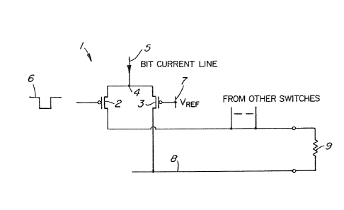
13 Figure 1 is a schematic diagram of a
14 circuit in accordance with the prior art, and
Figure 2 is a schematic diagram of the
16 basic present invention.
17 Figure 1 illustrates the basic prior art
18 circuit. A differential amplifier 1 which is formed
19 of first and second similar conductivity MOS
transistors 2 and 3 has a common source node 4
21 connected to a bit current line 5 (current source).
22 The bit current line is connected in common to other
23 differential amplifiers of similar structure. One bit
24 6 of a multiple bit word which is to be converted from
digital to analog form is applied to the gate of the
26 first transistor 2; other bits of the same word are
27 applied to corresponding gates of first transistors of
28 the other similar differential amplifiers.
29 A reference voltage VREF is connected
from a reference voltage line 7 to the gate of
31 transistor 3, and the drain of transistor 3 is
32 connected to ground 8, at voltage level Vss. The
33 drain of transistor 2 is connected to one terminal of
34 a load 9, while the other terminal of load 9 is
connected to ground 8. The drain of corresponding
36 transistors 2 are connected in parallel to the first
37 terminal of load 9, in common with the one shown.
38 - 3 -
.
' ' ' .
~3~29~6
01 As is well known, the current from bit
02 current line 5 is steered between the load and ground,
03 depending on the level of the digi-tal signal applied
04 to the gate o~ transistor 2. When the bit level is
05 lower than VREF by a sufficient margin, transistor 3
06 is rendered non-conductive and the current from bit
07 current line 5 passes through transistor 2 into the
08 load impedance. If the bit level exceeds the VREF
09 by a sufficient margin, then the current from the bit
current line 5 is switched to ground through
11 transistor 3.
12 As noted earlier, i-t is not an easy task
13 to cause the VREF to be a stable reference, devoid
14 of transients. Because of constant switching of
current through transistors 3 and 2, or not being
16 switched through the transistors, depending on the
17 level of the input signal bit 6, the potential at
18 common source node 4 varies significantly. Parasitic
19 capacitance unavoidably present at the common source
node 4 thus charges and discharges with the variation
21 in voltage, which creates transient errors in the
22 analog level of current switched into or out of the
23 load. This of course is multiplied by the number of
24 switches connected to the same load.
As an alternative structure to that
26 described with reference to Figure 1, sometimes the
27 inverse of the digital input signal is applied to the
28 gate terminal of the gate transistor 3, rather than
29 connecting the gate to VREF. While this achieves a
steady state constancy in the level of the common
31 source node 4, any time delay between the
32 complementary input signals to the gates of the two
33 transistors results in significant transient errors,
3~ such as both transistors being momentarily conductive
or non-conductive~
36 An embodiment of the present invention is
37 shown in Figure 2. In this embodiment transistors 2
38 - 4 -
. .
-: ' ' ' ~ , ' :
.:
:
,
~L~129~
01 and 3 are connected as a differential amplifier, with
02 a common source node 4 connected to a bit current line
03 5 as before. Transistor 2 is connected with other
04 similar circuits to load 9, as in the circuit
05 described above. ~owever in the presen-t invention
06 transistor 12, which is a complementary MOS
07 transistor, of opposite conductivity type to that of
08 transistor 2, is connected with its source-drain
09 circuit in series with the drain of transistor 3 to
ground 8. The digital input signal is connected in
11 common to the gate of transistor 2 and -to the gate o-E
12 transistor 12. In the embodiment shown, the gate of
13 transistor 3 is connected to ground 8.
14 In operation, when an input signal is at
low logic level, transistor 12 is cut off and
16 therefore no current can flow in transistor 3, even
17 with its gate texminal connected to ground as shown.
18 In this embodiment, there is no longer a need for an
19 intermediate reference voltage level VREF as
required in the prior art circuit. A large part of
21 the voltage change previously observed at the common
22 source node 4 is eliminated. Since a relatively
23 constant voltage at the common source node is
24 aehieved, the bit eurrent level remains relatively
eonstant. Since the voltage at the common source node
26 ~ is relatively constant, the parasitic capaci-tance
~7 at the eommon souree node has substantially reduced
28 charging and discharging, substantially reducing the
29 switching noise, since transient energy is
substantially reduced. Since transient energy is
31 substantially reduced, transient errors in the level
32 o~ the analog eurrent switched into or out of the load
33 is substantially reduced.
3~ Other similar cireuits are connected so
that eaeh has a separate bit of a multi-bit digital
3~ input word applied to the gate of eorresponding
37 transistors 2 and 12, and the drains of corresponding
38 - 5 -
~312~
01 transistors 2 are connected to the first terminal of
02 the load 9, on the leads labelled "Erom other
03 switches" in Figure 2.
04 In another embodiment, the gate of
05 transistor 3 is connected to some other fixed voltage
06 source, other than ground. Advantageously this can be
07 the same as either the low or the high level logic
08 state level of the digital signal source (a laboratory
09 prototype successfully utilized the low logic state
level).
11 Transistors 2 and 3 can be of P-type
12 conductivity and transistor 12 can be of N-type
13 conductivity, although the conductivity types can be
14 reversed, with appropriate power supply polarity
correction.
16 It should be noted that the circuit above
17 operates due to a novel use of CMOS transistors. It
18 cannot work using complementary bipolar transistors,
19 since if corresponding bipolar transistors were used,
open circuiting the collector terminal of bipolar
21 transistor corresponding to transistor 3 would only
22 have the effect of diverting the emitter current to
23 the base terminal of the device. By using CMOS
24 transistors however the near-simultaneous turn on and
off of transistors 2 and 12 ensures minimum transient
26 energy, and this switching is achieved without the
27 requirement of a separate reference voltage VREF
28 line.
29 A person skilled in the art understanding
this invention may now conceive of variations or other
31 embodiments using the principles of the invention
32 described herein. All are considered to be within the
33 scope of the invention as defined in the claims
34 appended hereto.
36
37 - 6 ~