Note: Descriptions are shown in the official language in which they were submitted.
- 1 ~ 3~2~
60412-1941
Back~ound of the Inventlon
The invention relates to apparatus for processing
relating to a stream of bitso
Bits in a stream that are transmitted from one processor
to another typically need to be filtered (i.e., analyzed to
determine what they mean) and processed in some manner based upon
the result of the filtering. E.g., in a computer network (e.g.,
as described in Tanenbaum, A.S., Computer Networks~ (Prentice-
Hall, Inc. 1981), pp. 10-28 ("Tanenbaum")), the filtering of an
incomin~ bit stream occurs in the lower layers of the network
processor at a node; if the incoming bits are identified as being
o~ interest to the node (e.g., having a destination address
associated with the node in an address field of a frame of bits),
the bits are stored and later used by upper layers.
In the local area network controller for Ethernet
("LANCE"), which is described in MOS Microprocessors and
Peripherals 1985 D _ Book, (Advanced Micro Devices, Inc., Sunny-
vale, California 1985) pp. 2-50 to 2-86 ("LANCE Specification"),
the 48-bit Ethernet address is analyzed in a bit-by-bit compare,
and ~rames that do not have addresses that match are discarded.
When an address matches all the way through to the last bit in
the address ~ieldl the frame is placed in data buffers for access
by the upper layers. The upper layers do not know which address
matched, only that one did. Thus the software associated with the
upper layers must repeat the entire compare process.
~ .
.
.', ~ . ' .
- ~ .
~ - 2 - ~3~2~7
Summary of the Invention
In one aspect the invention features in general
processing a bit stream by using a hardware comparator
that compares first predetermined bits of a bit stream
(e.g., a field of a frame), an index generator that
generates an index based on the states of the
predetermined bits, and a processor that accesses the
inde~ and processes a group of bits of the stream (e.g.,
a frame) in one of a plurality of different ways based
upon the index, The processor thus need not compare the
entire se~ of predetermined bits in order to determine
how the group o~ bits should be processed, but simply
accesses the index, which includes that information.
The comparison involves comparison against a table of
comparison values that are provided to the hardware
comparator, and one of a plurality of different tables
is provided in response to a table select control
signal, providing great flexibility in filtering the bit
~tream.
In preferred embodiments, the predetermined
bits that are compared could be, e.g., a destination
address field indicating the intended recipient, a
protocol field, or a field identifying a data
compression algorithm. There also could be comparison
of predetermined bits that identify a special message
relating to mana~ement of a processor, There can be
data buffers that receive and store portions of the bit
stream and descriptor storages associated with
respective data buffers for storing descriptor entries
~0 relating to the data stored in the data buffers; the
inde~es can be stored in the descriptor storages
associated with the data buffers for access by the .
processor. The comparator can be programmable to
compare different fields of the bit stream in response
:~.' - ' , '
- ' .
.. . .
1312~
-- 3 --
to a field select control signal; the field select
control signal can include a start signal location and a
length signal designating the length of ~he bit field to
be used in the compare; the processor can co~trol the
field select control signal. The tables can be selected
in response to a value generated as the result of an
initial comparison of a field. The comparisons can be
advantageously controlled without direct involvement of
a host computer by using a chip control state machine, a
memory state machine, and a table memory in which are
stored: tables of comparison values; entries
identifying the predetermined bits being compared;
entries indicating whether the group of bits should be
discarded and whether interrupts should be generated
upon completion of a comparison; entries indicating
further comparisons to be made; entries indicating
whether an index should replace the predetermined bits
in the bit stream; and entries indicating where the
group of bits should be routed (e.g., to a port to
~o another network or to a data buffer). The invention can
be employed in a bridge that has at least one port to a
different network, the index ldentifying the port; the
processor can translate the fields of the bits in one
network's protocol into another network's protocol.
~5 Ring buffers can be used to temporaril~ store bits of
the stream while the index is being generated.
In another aspect the invention features in
general processing source data bits using a hardware
comparator that compares predetermined bits of the
source data bits, an index generator that generates an
index based on the states of the predetermined bits, and
a processor that accesses the index and modifies the
source data bits in one of a plurality of different ways
~3~29~7
4 6041~-2199
prior to transmitting the source data bits as a stream of bits.
In preferred embodiments the index can identify transmit
data to be place din a frame to be ~ransmitted; the transmit data
are placed in a fxame at a field prescribed by a start location
signal and a length signal. The index could alternatively
identify a data compression algori~hm.
According to a broad aspect of the invention there is
provided apparatus for processing a stream of bits comprising
a hardware comparator that compares first predetermined bits
of said stream,
comparison input means to provide a table of comparison
v~lues to said hardware comparator for comparison with said
predetermined bits of said stream,
said comparison input means being programmable to
provide one of a plurality of different tables in response to a
table select control signal,
an index generator in communication with said comparator for
generating an index based on the states of said predetermined
bits, and
a processor for accessing said index and processing a group
of said bits in at least one of a plurality of different ways
based on said index~
According to another broad aspect of the invention there
i~s provided apparatus for processing source data bits for
trallsmitting comprising
a hardware comparator that compares predeter~ined blts of
said source data bits,
an index generator that generates an index based on the
,: , .,
.~ , ' : .
.
' ' :
131 ~7
~ a 60~12-~199
states of said predetermined bits, and
a processor for accessing said index and modifying said
source data bits in one of a plurality of different ways prior to
converting said source data bits to a stream of bits to be
transmitted.
According to another broad aspect of the invention there
is provided a circuit for filtering a stream of bits comprising
a hardware comparator that compares first predetermined bits
of said stream,
comparison input means to provide a table of comparison
values to said hardware comparator for comparison with said
predetermined bits of said stream,
said comparison input means being programmable to provide one
of a plurality of different tables in response to a table select
contol signal, and
an index generator for generating an index based on the
states o~ said predetermined bits,
said index indica~ing one of a plurality of different ways
that said group of bits is to be processed.
~0 According to another broad aspect of the invention there
~s provided a method of processing a stream of bits comprising
providing a table of comparison values to a hardware
~omparator for comparison with predetermined bits of said stream,
the table being provided depending on a table select control
~ignai,
comparing first predetermined bits of sald stream using a
hardware comparator,
generating an index based on the states of sald predetermined
.
~ '
"`^` ~3~ ~9~
4b 60412-2199
bits, and
accessing said index and processing a group of said bits in
at least one of a plurality of different ways based on said index.
Other advantages and features of the invention will be
apparent from the following description of a preferred embodiment
thereof and from the claims. The particular details of the
example of the preferred embodiment should not be cons~rued to
limit the scope of this invention.
Description of the Preferred Embodi~ent
The preferred embodiment will now be described.
Drawinqs
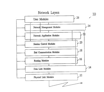
Fig. 1 is a block diagram of a node of a local area
network employing bit stream filtering according to the invention.
Fig. 2 is a block diagram showing a bit stream filtering
circuit and related components at a node.
Fig. 3 is a block diagram showing the bit stream
filtering circuit.
Fig. 4 is a diagram of a control entry and a table entry
used in bit stream filtering according to the invention.
Fig. 5 is a flow description of cache logic of a cache
state machine of the Fig. 3 circuit.
Fig. 6 is a flow description of chip control logic of a
chlp control state machine of the Fig. 3 circuit.
-~P
.
. .
.. . .
: . .
:.: . .. . :
:, .
- : . : , . ....
` -
- 5 ~ ~ 3i2~7
60~12-1941
Structure and Opera-tion
Referrin~ to Fig. 1, there is shown the network
architecture for node 10 of a local area network, as described in
Lauck, A.G., et al. "A Digital Networ]~ Architecture Overview",
Digital Technical Journal, Number 3, Sep~ember, 1986, pp. 10-24.
Node 10 includes physical link modules 12, data link modules 14,
routing modules 16, end communication modules 18, session control
modules 20, network application modules 22, network management
modules 24, and user modules 26. As is described in Tanenbaum,
the network is organized as a series of layers, each layer being
built on its predecessor and offering certain services to higher
layers and shielding those layers from the details of how the
o~fered services are actually implemented. In addition to communi-
cation between adjacent layers, there also are control lines
between nonadjacent layers.
Referring to Fig. 2, bit stream filtering circuit 28 (an
integrated circuit) resides in physical link modules 12 with LANCE
eatures 29 (as described in the LANCE specification) and serial
interface adapter l''SIA'') 31 connected to other nodes via an
Ethernet serial transmission line. Bit stream ~iltering circuit 28
filters, i.e., analysis, the incoming bit stream from SIA 31 to
~enerate an index indicating how the bit streams should be
~rocessed at the node. Bit stream filterin~ circuit 28 has access
to random access memory ("RAM") 30, which is also accessed by upper
la~ers and is controlled by host computer 32. Host computer 32
implements upper layers above physical link modules 12. Physical
link modules 12 and RAM 30 can thus be accessed and controlled by
upper layers. As is described in the LANCE specification, RAM 30
is used to provide memory
~ ' , .
.
- 6 - ~3~2~
locations for plural transmit and receive data buffers
45 (each buffer being used to store a ~rame, or portion
of a frame, that has been received or will be
transmitted) and descriptor storages for associated
descriptor entries 47 that have pointers to respective
data buffers ~5 and characterize the data stored in the
respective buffers 45. The LANCE descriptor entries
have been extended to include control entries 60
(described in Fig. 4) relating to bit filtering
according to the invention. Each descriptor entry
potentially can have a plurality of associated control
entries 60.
Referring to Fig. 3, bit stream filtering
circuit 28 includes write-through ring buffers 34 for
receiving a stream of bits over serial input line 36.
Ring buffer select control is controlled by chip control
state machine 38 to control routing of the bit stream to
one of three ring buffers 34, which operate essentially
as three shift registers that are each long enough to
hold an Ethernet frame (1536 8-bit bytes). The output
of ring buffers 34 is connected to serial transmitter 40
(for transmission of a serial bit stream to a separate
network) and/or to serial-to-parallel converter 44. The
data received from ring buffers 34 are provided by
~5 converter 44 in a parallel form for transfer through
buffer decode and con~rol line 42 to RAM 30.
Comparators 52 are controlled by chip control
state machine 38, The bits traveling through a ring
buf~er 34 can be routed from a location between the ring
buffer's input and output to pass through comparators 52
and be returned to the ring buffer 34 and continue
traveling through it. Hardware comparators 52 compare
predetermined bits (i.e., a field) with compare values
loaded in table entries 62 in ~able cache memory 58 and
.
~ 7 - ~3~2~7
indicate the results of the compares to chip control
state machine 38. Chip control state machine 38
includes an index generator ~unction to generate a
16-bit index based on the results of the compares. The
index is stored in table cache memory 58 in the result
field (Fig. 4) of a control entry 60 associated with the
descriptor entry 47 for a data buffer 45 assigned to an
incoming frame. Table cache memory 58 is controlled by
cache state machine 54. Table cache memory 58 and cache
state machine 54 thus comprise a comparison input means
to provide a table of comparison values to comparators
52.
In operation, prior to receiving a frame (for
example, from another node on the local area network) on
serial input line 36, a control entry 60 is read from
R~ 30 into table cache memory 58 via buffer decode and
control line 42. The control entry (Fig. 4) includes
"start bit`' (identiying the start location of the field
to be used for the compare), "length" (indicating the
2a length of the field being compared), 2-bit '`control" (to
control chip actions after filtering has been completed:
e.g., discard on false address comparison, interrupt
host when finished), "table pointer" (identifying a
table of comparison values to be stored in table cache
memory 58 and used in the compare), and "result`'
(storage locations for receiving the 16-bit index). The
descriptor entries 47 (including their control entries
60) stored in RAM 30 are determined by upper layers.
Prior to receiving the frame, up to three tables of
comparison values are stored in table cache memory 58 to
be used by hardware comparators 52. The table pointer
is used to ~etch a table stored in RAM 30 and store it
~s the table entry 62 in table cache memory 58
associated with the control entry 60. The table pointer
~ 8 - ~3~2~ ~
entry is thus used to generate a table select control
signal used to select the table of comparison values.
Table entries 6~ (Fig. 4) include 14 comparison values
(e.g., 48 bits if indicating Ethernet address) to be
8 used by comparators s2 designated 1 to 14 in Fig. 3, and
a further comparison value for use by a special
comparator, discussed in detail below. Associated with
each comparison value are (Fig. 4) an "enable" bit
(indicating whether the value is to be used; e.g., there
may be less than 14 comparison values in the table), and
a 4-bit '`link pointer" pointing to a further control
entry 60 to be used in a further compare depending upon
the results of an initial compare. Up to two link
pointer entries can be used to identify two further
control entries 60 to be initially fetched and stored in
table cache memory 58. "Output select" indicates where
to route the frame depending on the results of the
compare~ "Field replace" indicates whether the index
generated should replace the field compared in the bit
~0 stream. If the first table entry 62 does include one or
more table pointers identifying further control entries
60, they are fetched and stored in table cache memory
58, as indicated in the cache logic described in Fig. 5.
Node 10 can receive both Ethernet frames and
2~ frames meeting IEEE Standard 802.3 ~"802.3 frames").
When the frame is received over input line 36, the frame
goes into one of three ring buffers 34 as determined by
chip control state machine 38. As indicated in the chip
control logic described in Fig. 6, chip control state
3~ machine 38 uses the start bit and length of the control
entry 60 to identify start and stop bits of the field
compared by hardware comparators 52, which then compare
the bits in the field identified as the bits are routed
from a ring buffer 34 through comparators 52. The start
.
9 ~3~L%~ ~
bit and length bit stored in con-trol entry 60 are thus
used to generate a f ield select control signal to
determine the field of bits that is compared. The bits
are compared with bits of the co~parison values of the
table entry 62 in table cache memory 58, and a 16-bit
index is generated by chip control state machine 38.
For example, if the field being compared is the 48-bit
destination Ethernet address, the table would include as
values the 14 48-bit physical addresses that can be
associated with node 10. The inde~ is deposited by chip
control state machine 38 in cache state machine 54,
which in turn places the index in the result field in
the respective control entry 60 in table cache memory 58.
Assuming the frame is to be temporarily stored
in a data buffer 45 in RAM 30 and used by the upper
layers at the node, the frame, upon leaving a ring
buffer 34, is passed through serial-to-parallel
converter 44 and buffer decode and control line 42 to
the respective data buffer 45 in RAM 30. The result
~o (index) of the control entry in table cache memory 58 is
also placed in RAM 3Q, in the associated descriptor
entry 47, which points to the respective data buffer
45. Synchronization and clocking of state machines 38,
54 are provided by the incoming bit stream, as indicated
~5 by synch line 57.
If the destination address does not match up
with any of the 14 addresses in the table, the frame
will be handled as determined by the state of the
control field in control entry 60; e.g., the frame could
be discarded. At the end of the compare, if the control
field of the control entry 60 indicates interrupt, an
interrupt is generated by chip control state machine 54
and provided to host 32. If the field replace entry of
the table entry 62 is true, and, if there is a match,
o- ~3~2~
the index is used to replace the field that was compared
in the frame.
The special comparator 52 (designated "0") is
used to compare the 4-by~e ield in the incoming frame
that is used either to indicate the length of the frame
(if an 802.3 frame) or to identify protocol (if an
~thernet frame) to determine if the frame is an Ethernet
frame or an 802.3 frame. If the value is less than or
equal to the maximum length for an 802.3 frame, then the
13 frame is identified as an 802.3 frame; if not, the frame
is assumed to be an Ethernet frame; by convention all
Ethernet protocol identifying numbers are greater than
the maximum 802.3 frame length. The result of the
special comparator can thus be used to select either the
second table or third table in table cache memory 58 to
be used in a further field comparison.
The initial index or the special comparator
output thus might indicate that there should be a
further compare on a different field using the second or
~0 third table stored in table cache memory 58, which table
and field had been identified by link pointers and
preloaded. Host 32 thus need not be interrupted, and
different frames could be compared in different manners
based upon the result o~ an initial compare without
intervention by the host. A result (i.e., index) of an
initial comparison can be stored in RAM 30 shortly after
~he initial comparison has been completed and before a
~rame has passed through ring buffers 34 and into a data
buffer 45. At this time the associated tahle entry 62
and control entry 60 are no longer needed and can be
deleted from tabl~ cache memory 58. The next comparison
~ill use one of the two other table and control entries
already stored, and the freed-up space in table cache
memory 58 can be filled by a further table entry 62 and
~,
3~2~
control entry 60 according to the cache logic of Fig.
5. The further control entry 60 and table entry 62 to
be loaded are identi~ied by an enabled link pointer in
the presently used table entry 62. The results of the
further comparison can also be stored in a descriptor
entry 47 in RAM 30 and can be used to identify further
comparisons. If necessary to do further compares, the
frame can be fed back from a ring buffer output to a
ring buffer input.
The upper layers of the node shown in Fig. 1
can access the data stored in RAM 30 and employ the
indexes in the descriptor entry 47 to assist in and
speed up processing. The upper layers thus function as
a processor that accesses the index and processes bits
in the frame in at least one of a plurality of different
ways based on the index. For example, if the index
identifies a destination address, there is no need to do
a 48-bit software compare of the field of the
destination address. The index could also identify a
~a protocol which would be used by one of the upper layers
in processing the data stored in the data buffer. The
index could also identify a data compression algorithm,
and an upper layer would expand the data acco~ding to
the algorithm identified. The index could also indicate
2~ that the frame is to be transmitted via serial
transmitter 40, acting as a bridge, to another network.
In this case the use of three ring buffers 34 permits
storage of a later frame while an earlier frame is being
serially transmitted by transmitter 40 at a lower rate.
Serial transmitter 40 can translate fields as bits pass
through it. Comparators s2 could also identify a
special message and generate an index related to
management of the network and not related to a frame to
be processed.
:
. . ., ~ ~. ,
~ 12 ~312~ ~ 60412-1941
Other Embodiments
Other embodiments of the invention are within
the scope of the following claims. For example, the
comparison values could be generated by other means, the
indexes could be used to process the bits in other ways,
and ~he comparator output could be the index, in which
case the comparator would also be unctioning as an
index generator.
Also, a hardware comparator could be used to
process source data bits from upper layers before
transmitting them. The comparator compares
predetermined bits of the source data bits and generates
an index used by a processor to modify the source data
bits before transmitting them as a stream of data bits.
E.g., the index can identify transmit data to be placed
in a frame to be transmitted; the transmit data are
placed in a frame at a field prescribed by a start
location and a length signal. The index could
alternatively identify a data compression algori~hm.
~0