Note: Descriptions are shown in the official language in which they were submitted.
-
1312965
APPAR~TUS FOR MEASURING THE PEAK
VO_TAGE APPLIED TQ A RADIATION SOURCE
Field of the Invention
This invention relates to the art of radiation
measurement and, more particularly, to measuring the peak
voltage applied to a radiation source, such as an X-ray
generator, by monitoring the generated radiation.
~ g~ the Invention
The calibration of an X-ray machine is impor~ant in
diagnostic radiology. The measurement of the potential
applied to an X-ray machine has been recognized as an
important variable in the production of high quality
diagnostic X-ray films. In the United States, the Radiation
Control for Healthy and Safety Act of 1968 became law in
1973. The main intent of the law was 'co protect the
population from unnecessary radiation exposure.~ One way to
accomplish this is to reduce the number of retakes of
X-rays. The law requires that~X-ray machines meet certain
-2- 1 3 1 2965
requirements. One of these requirements is that the
maximum applied input voltage, sometimes referred to as the
peak kilovoltage (kVp), applied to the X-ray machine fall
within certain limits specified by the manufacturer. If an
X-ray machine is inaccurately calibrated, this may result
in shortened component life and poor quality X-rays, which
ma~ result in retakes. Consequently, there is a need to
periodically check the accuracy of the kVp setting on X-ray
machines and recalibrate when required.
Diagnostic X-ray machines operate at relatively high
voltages, such as on the order of 50 kV to 150 kV. Direct
measurement of such a high voltage may be dangerous and has
in the past been accomplished by disconnecting the high
voltage circuits and reconnecting a high voltage divider
having two large value resistance sections connected
between the anode of the X-ray generator and ground and
between the cathode of the generator and ground. The high
voltage divider circuit is typically large in volume and
size and the operation for measuring the high voltage in
such apparatus is time-consuming and only qualified service
personnel could accomplish this task. Hospital staff
people have not normally been employed for conducting this
test because of the size and weight of the dividér circuit
and the inherent danger involved in making such a
measurement
Alternatives to the direct measurement, utili2ing a
high voltage divider as discussed above, are various
:....
'
-3- 1312965
noninvasive measurement techniques presently being
employed This includes the use of a noninvasive film
cassette, as well as a noninvasive electronic device
employing filters and sensors. These noninvasive
techniques measure the input voltage to an X-ray machine
Erom measurements of the radiation the machine emits.
The film test cassettes (sometimes known as the Adrian
Crooks or Wisconsin test cassette~ have been used to
determine the input kilovoltage to a radiation source from
the measurements of the radiation it emits. A test
cassette is placed in the field of an X-ray beam and
operates on the principle that the extent of attenuation of
an ~-ray in a material, such as copper or aluminum, is
related to the kilovoltage applied to the X-ray tube.
X-ray film is exposed to X-rays that have been attenuated
while passing through multiple layers of material including
a copper sheet and a sheet that includes copper disks and
holes. The measurement requires the assistance of skilled
technicians, development of the film and reading of the
film with a densitometer. The accuracy of this method is
on the order of + S kV. Moreover, since such a test
cassette can measure only the e~fective or average kV and
not the true peak of the waveform, results will not reveal
significant ripple or spiking on the waveform.
Another noninvasive device for measuring input voltage
supplied to an X-ray machine takes the form of an instrumen~
. . - ~ . ., - . ..
1 31 2~65
known in the art as a kVp meter. Examples of such meters
are disclosed in various U.S. patents, including the
patents to Zarnstorff et al., 4,697,280, Siedband,
4,361,900, as well as products manufactured by Keithley
Instruments, Inc. as model Nos. 35070 and 35080. In
general, these kVp meters operate on the principle of
passing an X-ray beam through a pair of copper filters
positioned side-by-side so that the X-ray beam is
attenuated as it passes through each filter. The two
filters are of different thicknesses and, hence, as the
radiation passes through each filter, it is attenuated
dif~erently. The attenuated radiation from each filter is
then detected by a pair of X-ray detectors, such as solid
state photodiodes, which provide output electrical signals
having magnitudes which depend upon the attenuated
radiation levels from the two filters. A ratio of these
two signals is then made. This ratio will ~ary with the
input kilovoltage applied to the X-ray tube. The X-rays
passing through the thicker material increase faster with
increasing input kilovoltage than the X-rays passing
through the thinner material. Consequently, the ratio of
the signals representative of radiation passed through the
thick material to that of the thln material starts at zero
and increases as the kilovoltage increases. For very large
kilovolts, the ratio approaches unity. These kVp meters
typically operate over a range from 50 to 150 kV.
.~ ' ' ' ..
~ 3 1 2965
Recently, there has been significant interest dealing
with mammography. This is the X-raying of the female
breast to locate cancer at an early stage. Unlike a
typical diagnostic X-ray machine, which operates in the
range of 50 kV to 150 kV, the mammographic X-ray machines
operate at a somewhat lower voltage level on the order of
25 kV to 40 kV. Another significant distinction is that
the mammographic X-ray machines usually employ molybdenum
anodes as opposed to the tungsten anodes which are used in
diagnostic X-ray machines operating in the range oE 50 kV
to 150 kV~ The use of molybdenum anodes for these lower
voltage mammographic X-ray machines presents problems in
attempting to measure the operating voltage with the
typical kVp meters discussed hereinabove.
It has been determined that the photon spectrum for
molybdenum in the mammographic region differs substantially
from that of tungsten. Thus, in this region the photon
spectrum for tungsten is a somewhat smooth inverted
U-shaped curve, whereas that for molybdenum has a
substantial discontinuity near the K edge o the anode
material ~approximately 20 kilovolts for molybdenum).
Moreover, such a molybdenum anode will fluoresce at
discrete energies on the order of 17.5 kV and 19.5 kV.
Also, it is customary to employ additional filters made o~
molybdenum in a molybdenum X-ray machine which causes
further suppression in the higher energy spectrum. As a
-6- 1312965
consequence, the ratio technique employed by the kVp
meters, as discussed above, does no~ provide an adequately
accurate measurement of the operating voltage of such
mammographic X-ray machines.
The present invention is directed toward determining
the operating voltage of an X-ray machine with an accuracy
that is independent of the anode material. Thus, in the
example given, the measurement is independent of whether
the anode material is molybdenum or tungsten.
The present invention is based on the recognition that
a chemical element, such as molybdenum or tungsten,
exhibits an absorption phenomenon. Such elements when
irradiated by an X-ray beam will absorb radiation at a
predictable rate until the voltage applied to the X-ray
machine attains a particular level and tllen a sudden
transition takes place in the absorption rate. This
transition is a sharp increase in the absorption rate and
it corresponds with what is known as the K absorp~ion edge
of that particular chemical element. The K absorption edge
refers to the K quantum shell. An electron can be removed
~rom the K shell by photoelectric absorption. This takes
place when photons of a sufficiently high energy level are
incident upon an atom causing an electron to be ejected from
the K shell. The threshold photon energy to acrhieve this
is known as the K-absorption edge. Similar discontinuities
are present in the L quantum shell as well as in the ~
. ~ . . .
. .
,
- ~
-7- 1312965
quantum shell. However, elements have only a single sharp
transition absorption edge in the K quan~um shell. On the
other hand, elements exhibit multiple absorption edges in
the L quantum shell and in the M quantum shell. It would
be difficult to determine from such multiple transitions
the correct level o~ photon energy requlred to achieve the
transitions. For this reason, it is believed that a more
accurate determination of the photon energy level required
can be made from sensing only the K-absorption edge.
.5,
patent to G. R. Harris et al., 3,766,383 discloses
an apparatus for calibrating the kilovoltage of a
diagnostic X-ray generator by placing a chemical element or
test sample, having a known K-absorption edge, within an
X-ray beam. The test sample is disposed at an angle o~
approximately 45 degrees to the generated radiation path so
that some energy is re~lected as scattered energy, and some
energy is transmitted through the sample as transmitted
energy. The scattered energy and the transmitted energy
are detected and a ratio is calculated as to the
transmitted and scattered detected radiation values. When
this ratio changes significantly, it is indicative that the
K-edge has been reached. Since the sample has a known
K-absorption edge, this in~ormation is then used to
determine the kilovoltage level.
The system proposed by Harris is awkward in its
implementation. Because both the scattered as well as
- ,
-8- 1312965
transmitted X-rays are detected, the detectors themselves
must be positioned in different planes, one located in a
plane above the test sample, and one located in a plane
below the test sample. The structure to accomplish this
would be relatively expensive and cumbersome in its
implementation In addition, the Harris system proposes
the monitoring of the detector ratio as a function of the
kilovolts applied, and this takes the form of an inverted
V-shaped curve with an upsloping ramp which reaches a peak
at the K-absorption edge of the test sample, and then a
downward slope after the K-absorption edge has been
exceeded. Consequently, the kilovoltage is a double valued
function of the detector ratio. ~hat is, there are two
kilovolt levels for each detector ratio level, and, hence,
for a single exposure or single reading, the operator would
not know if the kilovoltage level at that ratio level is
above or below the K-absorption edge~
Summary of the Invention
It is an object of the present invention to provide an
apparatus for determining the peak voltage applied to a
radiation source which apparatus operates independently of
the anode material employed in generating the radiation.
It is a still further object of the present invention to
provide an apparatus for measuring peak voltage applied to a
radiation source which apparatus operates independently of
,. , ":.,.:.,~ , .,,.:
1 3217~
the absorbing material which may be present in the X-ray path.
It is a still further object of the present invention to
provide such an apparatus which does not rely on detecting
scattered and transmitted radiation as proposed by Harris,
supra.
In accordance with the present invention, apparatus is
provided for measuring the peak voltage applied to a radiation
source operating at a variable input voltage. This apparatus
includes a set of radiation absorbing filters with the first
ilter constructed to include at least a first chemical element
that exhibits a known K-absorption edge, and a second filter
which includes at least a second chemical element chosen so that
the first and second elements exhibit essentially the same
radiation absorption characteristics for photon energies below
the K-absorption edge of the first element but substantially
different characteristics above the known K-absorption edge.
These filters are then positioned within the radiation emitted
by the radiation source so as to be simultaneously irradiated by
the source, the radiation impinging upon a surface of each
element. This radiation is partially absorbed as it passes
through the elements so as to exit therefrom as attenuated
radiation. The attenuated radiation passed by the first
and second filters is detected for purposes of providing an
output indication when the radiation passed by the filters is
differently attenuated. This indicates that the K-absorption
edge of the first element has been exceeded and
. ~ .
.
-lo- 1 3 1 2965
this is indicative of the magnitude of the voltage applied
to the radiation source.
In accordance with another aspect of the present
invention, a detector in the form of a radiation sensitive
film is positioned such that the filters are located between
the radiation source and the film. The film records two
images having densities respectively representative of the
total amoun~ of the attenuated radiation passed by the first
and second filters. The densities of the images will be the
same unless the K-absorption edge of the first filter has
been exceeded.
In accordance with a still further aspect of the
present invention, the detector takes the form of a pair of
radiation sensitive photoelectric means, such as
photodiodes, positioned such that the first and second
filters are located intermediate the radiation source and
the photodiodes. These photodiodes will provide output
electrical signals which will be of essentially the same
magnitude until the K-absorption edge of the first filter
has been exceeded whereupon one of the signals will be
greater than the other. This difference in electrical
signals may be observed as with a signal comparison means
which may activate a visual output indicator, such as a
light-emitting diode (LED), ~or providing a visual output
indicative that the K-absorption edge of the first filter
has been exceeded.
- . . :,
. . .: ' : '
.' ' ~', - ' ' ' ' ' ' '~ :
-11- 1 31 2~65
Still in accordance with the invention, a plurality of
sets of radiation absorbing filter means are provided with
each set including a first element and second element. The
first elements include different chemical elements having
different known l~-absorption edges in the voltage range of
interest. The second elements are chosen so that the
elements exhibit the same radiation absorbing
characteristics for photon energies below the K-absorption
edge of the first element. The detector means may take the
form of a radiation sensitive film or an array of photo-
sensitive detector means, such as photodiodes, for providing
output indications when the K-absorption edge of one or more
of the sets has been exceeded.
Brief Description of the Drawings
The foregoing objects and advantages of the invention
will become more readily apparent from the following
description of preferred embodiments of the invention as
taken in conjunction with the accompanying drawings which
are a part hereof and wherein:
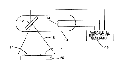
Fig. 1 is a schematic illustration showing one
application of the invention for measuring the input
voltage applied to an X-ray tube;
Fig. 2 is a waveform showing attenuation with respect
to energy for purposes of illustrating the K-absorption
edge of a chemical element;
~`
~ .
.
.
-- 1 3 1 2q65
-12-
Fig. 3 is a waveform of voltage with respect to time
illustrating the input voltage applied to an X-ray tube;
Fig. 4 is a wave~orm of ratio with respect to time
showing that a squarewave results as long as the operating
voltage is less than the K-absorption edge of the chemical
element being employed;
Fig. 5 is a view similar to that of Fig. 3, bu~ showing
the level of the operating voltage as exceeding the
K-ahsorption edge;
Fig. 6 is a waveform similar to that of Fig. 4, but
showing spikes on the waveform indicative that the
K-absorption edge has been exceeded;
Fig~ 7 illustrates an array of matched sets of filters
mounted on a phantom in accordance with one embodiment of
the invention;
Fig. 8 is a view taken from Fig. 7 looking in the
direction of the arrows 8-8;
Fig. 9 is a perspective view illustrating the phantom
of Fig. 7 placed on top of a film cassette;
Fig. 10 is an illustration of the developed X-ray film
taken from the film cassette-o~ Fig. 9 and showing
variations in intensity of recorded images;
Fig. 11 illustrates another embodiment of khe invention
wherein the phantom of Fig. 7 is placed on top of a housing
containing photodiode sensors and light-emitting diodes for
indicating that the operating voltage has exceeded the
~-absorption edge of one or more filters;
;
~' .
. - :
: .
-13- 1312q65
Fig. 12 illustrates the electronic circuitry employed
within the housing of Fig. 11;
Fig. 13 is an embodiment similar to that of Fig. 11,
but showing the phantom of Fig. 7 placed on top of a
housing containing a digital read out display; and
Fig. 14 illustrates the electronic circuitry employed
within the housing of Fig. 13.
Description of Preferred Embodiments
Referring now to Fig. 1, there is schematically
illustrated an X-ray tube 10 having an anode 12 and a
cathode 14. The anode 12 and the cathode 14 are connected
to a variable kilovoltage X-ray generator 16 in a
conventional fashion. The X-ray generator 16 is provided
with means for supplying a variable kilovoltage to the X-ray
tube over a range such as on the order irom 10 kilovolts to
150 kilovolts. The intensity of the X-ray beam 18 generated
by the X-ray tube varies with the setting of the variable
kilovoltage supplied by the generator 16. The present
invention is directed toward calibrating this input voltage
by a noninvasive means for determining the peak kilovoltage
applied by measuring characteristics of the X-ray beam 18.
In accordance with the invention, a pair of filters Fl
and F2 are p,ositioned within the field of energy of the
X-ray beam 18. These filters Fl and F2 may be identical in
size and shape, such as rectangular slabs or circular disks,
and which preferably ~for ease o~ design and construction)
-14- 1 3 1 29 65
lie flat in the same plane so that radiation from the X-ray
tube impinges upon a flat surface of each filter. Assume
for the moment that each filter exhibits the same radiation
absorbing characteristics. Radiation that passes through
each filter will be attenuated by the same amount and a
detector 20 monitoring the attenuated radiation exiting
from each o~ the filters will note that the intensity of
the attenuated radiation is equal. The detected attenuated
radiation exiting from the two filters F] and F2 may be
converted into electrical signals of the same magnitude.
The ratio of the two signals would be unity (or the
difference would be zero). If the detectors are not of the
same size or sensitivity, the ratio would be a constant but
not equal to one.
The detector 20, for the purposes discussed thus far,
may take the form of a film cassette including an X=ray
film which will record two images for the attenuated
radiation respectively passing through filters Fl and F2.
The exposed film may be developed and the two exposed
images may be examined with a film densitometer. So long
as the attenuated radiation exiting from each filter is of
the same intensity, the density of the two images will be
the same. Alternatively, the detector 20 may include a
photodiode associated with each filter for providing an
electrical output signal indicative of the intensity of the
detected radiation passed by the filter. Electrical
circuitry may serve to provide an output in accordance with
' ~ -, ' ` , :
.~
: .
-15- 1 31 2965
the ratio of the detected radiation passed by filter Fl to
that of the detected radiation passed by filter F2 .
(Alternatively, the difference between the two may be
taken.)
In accordance with the present invention, the radiation
absorbing characteristics or the attenuation rate of
filters Fl and F2 is identical up to an energy level that
corresponds with a particular voltage V0 which, in turn,
is representative of a particular input kilovoltage applied
to the X-ray tube. Until this level is reached, the
difference or the ratio of the outputs ~rom the filters will
be the same. However, once this level has been exceeded,
the difference between detected attenuated radiation from
the filters will be greater than zero and the ratio will
different than 1. This voltage level V0 corresponds with
the K-absorption edge of filter F2. The voltage range of
interest may be from approximately 18 kV to 4~ kV, suitable
for mammographic X-rays. Within this range, the
K-absorption edge for tin is 29.200 kV. On the other hand,
the chemical element copper does not have a K absorption
edge within this range. Copper has a K-absorption edge at
8.979 kV. Since almost no energy will be transmitted
through the filters at 8.979 kV, filter F2 may be
constructed from chemical element tin, whereas filter Fl
may be constructed from the chemical element copper.
The thicknesses of filters Fl and F2 are adjusted so
that they have identical attenuation characteristics below
~ ~ '
-16- 1312965
the K edge of tin (filter F2). By so constructing filters
Fl and F2, the outputs as detected by detector 20 will be
equal until the input kilovoltage applied to the X-ray tube
exceeds the K-absorption edge of tin (filter F2). At that
point, the outputs will be different. If the detector 20
includes an X-ray film then, upon exposure, the image for
filter F2 will not be as dense as that for filter Fl,
because of the sharp increase in attenuation at the
K-absorption edge for tin (at 29.200 kV). Consequently, a
single exposure would provide the operator with information
as to whether the operating voltage applied to the X-ray
tube is below or above that of the K-absorption edge of
filter F2, in this case 29.200 kV for tin.
The foregoing may be better appreciated with reference
to Fig. 2, which shows a graphical illustration o
attenuation versus energy when a chemical element is
exposed to an X-ray beam, such as beam 18. As the photon
energy increases, the attenuation decreases until the
K-absorption edge for that chemical element is reached. At
that point, there is a sudden increase in the attenuation,
as is seen from Fig. 2. Consequently, if filters Fl and F2
exhibit the same attenuation characteristics until the
photon energy exceeds the K edge of filter F2, the radiation
exiting from the filters will be equal. Once the K edge
has been exceeded, then the radiation exiting from filter
F2 will be attenuated by a greater amount than that of the
cadiation exiting from filter F2. If this be recorded on an
- ~ ,
.
, . : . , ' ~ ',. ' . . `
-17- 1312965
X-ray film, then the images for filter F2 will be less dense
than that for filter F1. Thus, the present invention, in
its broader aspects, provides a means for noninvasively
determining from a single reading or exposure as to whether
the input kilovoltage is above or below a particular level
associated with the K-absorption of filter E~2 (in this case
29.200 kV for tin).
The invention contemplates that an array of matched
filter sets be employed, each including a filter F1 and a
filter F2. A plurality of filters F2 may be used with each
taking the form of a different chemical element having a
K-absorption edge within the voltage range of interest (in
this case from 15 kV to 40 kV). The corresponding
plurality of filters Fl may each be of the same chemical
element, such as copper and/or aluminum.
Several matched filter sets, each including a copper
and aluminum filter and a filter constructed of a chemical
element having a K-absorption edge in the vol~age range of
interest have been tested using the Keithley Model 35080
kVp divider and an oscilloscope to provide a measurement of
kilovoltage with respect to time and to provide an output
representative of the ratio of the attenuated radiation
passing through filter Fl to that passing through filter F2.
In each case copper and aluminum element:s were used for
filters Fl and different chemical elements were used for
filters F2. The experiments for filters F2 included silver
(K-absorption edge of 25.Sl4 kV), indium (K-edge of 27.940
'
-1~- 1 3 1 2965
kV), cadmium (K-edge of 26.711 kV) and tin (K-absorption
edge of 29.200 kv). The operating voltage for a single
phase X-ray ~enerator appeared as shown in Fig. 3. The
ratio with respect to time is shown in Fig. 4 and it is
seen that a squarewave with a flat top is presented. The
operating voltage was then increased, as is seen in Fig.5,
so that the peak voltage exceeds the K edge of filter F2.
The result is a spike 30 on the ratio waveform of Fig. 6.
The spikes 30 provide information that the K edge o filter
F~ has been exceed and this provides an absolute
calibration of the X-ray machine. In addition, the spike
is roughly proportional to the amount by which the K-edge
is exceeded and 'chus can be interpolated for further
accuracy. The operation which ensues is independent of the
anode material, i.e., for example~ whether the anode
material be tungsten or molybdenum. Table I below presents
a listing of suitable chemical elements for filters F2
within the range from 15 kV to 40 kV.
TABLE I
Element K Edge
Mol~bdenum 19.999 kV
Rhodium 23.220 kV
Palladium 24~350 kV
Silver 25.514 kV
Cadmium 26.711 kV
Indium 27.940 kV
Tin 29.200 kV
Antimony 30.491 kV
Iodine 33.169 kV
Cesium 35.985 kV
Barium 37.411 kV
-19- 1312q65
The elements presented in Table I all have K-absorption
edges in the range between 15 kV and 40 kV. Consequently,
all of these elements fall within the voltage range at
which mammographic X-rays are taken. These elements may be
employed for calibrating the peak kilovoltage applied to an
X-ray tube used in mammography. The invention, however,
can also be applied in the diagnostic region, which is on
the order of from 50 kV to 150 kV. Some chemical elements
which may be employed in the diagnostic region and their
R-absorption edges are presented below in Table II.
TABLE II
Element
-
Gadolinium 50.240 kV
Erbium 57.486 kV
Tantalum 67.414 kV
Tungsten 69.524 kV
Platinum 78.395 kV
Gold 80.723 kV
Mercury 83.103 kV
Lead 88.006 kV
Array of Matched Filter Sets
Reference is now made to Fig. 7 which illustrate an
embodiment of the invention employing an array of matched
filter sets, each set including a pair of filters that
correspond with filters Fl and F2 of Fig. 1. In this
embodiment, howe~er, each of the filters from the different
sets that correspond with filter Fl may all be of the same
chemical element. Thus, there are five Fl filters
-20- 13129~5
illus~rated in Fig. 7 and are identified as filters FlA
through FlE. Each of these filters may be constructed of a
particular chemical element, such as copper or aluminum. On
the other hand, the filters corresponding to filter F2
include filters F2A through F2E. Each of these filters is
constructed from a different chemical element that does have
a K-absorption edge within the range of interest.
Preferably, these filters have K-absorption edges which are
chosen to provide a sequence through the range of interest.
For example, with reference to Table I, the elements to be
employed for filters F2A through F2E may be of the following
sequence: silver, cadmium, indium, tin and antimony. This,
then, represents K-absorption edges of 25.51~ kV, 26.711 kV,
27.940 kV, 29.200 kV and 30.4~1 kV for filters F~A through
F2E, respectively. The filters may be mounted on a suitable
holder or phantom 40, which may be constructed of a material
which is essentially opaque to X-rays, such as steel or
lead. This may be accomplished by providing a series of
holes in the phantom and then mounting each filter in the
manner as shown in Fig. 8 where filters FlC and F2C are
illustrated as flat elements having an upper surface which
may be exposed to X-rays impinging thereon from an X-ray
machine. The elements may be held in place as with a
suitable bonding or the like. ``
In application, the phantom 40 (Fig. 7) may be placed
on top o~ a ~ilm cassette ~2 containing a sheet of X-ray
-21- 1 31 2 q 65
film and an appropriate intensifying screen. The upper
surface of phantom 40 is then exposed to an X-ray beam which
irradiates each of the filter sets so as to expose the film
to the radiation. The exposed ~ilm is then developed and
the sets of exposed areas are examined with a film
densitometer. The developed film 44 is illustrated in Fig.
10 which shows recorded images. These images correspond
with the matched pairs of filters shown in Fig. 7. Thus,
as seen in Fig. 10, recorded images RlA and R2A correspond
with the matched set of filters Fla and F2A. Similarly,
recorded images RlB and R2B correspond with filters FlB and
F2B. In a similar manner, recorded images RlC, R2C and
RlB, R2D, and RlE, R2E correspond to the other sets of
matched filters in Fig. 7.
In the example shown in Fig. 10, the density levels are
different for the recorded images RlA and R2A and are also
different for the recorded images RlB and R2B, as is the
same case with recorded images RlC and R2C. However, it
will be noted that the densities are the same for recorded
images RlD and R2D and RlE and R2E. This means that from a
single exposure of an X-ray film to an X-ray beam, the
operator knows that the peak kilovoltage was greater than
that for the K-absorption edge level of filter F2C, but less
than that of the K-absorption edge of filter F2D, Since the
K-absorption edges for these filters are known from Table Il
it can be concluded that the peak kilovoltage applied to the
, .
-22- 1 31 2q65
X-ray tube was between 27.940 kV and 29.200 kV an~ could be
approximated by 28.57 ~ 0.63 kV. From a single exposure,
then, the operator can determine the peak kilovoltage
applied to the X-ray tube within 0.63 kV, in the example
being given. This is a substantial improvement over prior
art methods of determining peak kilovoltage which have an
error factor on the order of ~ 1.5 kilovolts or more.
Attention is now directed to Figs. 11 and 12 which
illustrate an embodiment of the invention in which an
photodiode array is substituted for the film 44 of Fig. 10.
In the embodiment of Fig. 11, the phantom 40 may be
constructed as described hereinbefore with re~erence to
Figs. 7 and 8. In this embodiment, the detector fcr
detecting the peak kilovoltage may take the form of an
electronic photodiode array 50, as opposed to the film ~
of Fig. 10. The array includes a housing 52 which contains
sensors SlA through SlE aligned so as to be in registry
with filters FlA through FlE when the phantom ~0 is placed
in registry on top of the array 50. Similarly, housing 52
contains sensors S2A through S2E which are aligned with
filters F2A through F2E. Each sensor takes the form of a
photodiode which is responsive to the radiation impinging
thereon to provide an output current having a magnitude in
accordance with the level of intensity of the received
radiation. In addition to the radiation sensors, the
housing 52 also contains electronic circuitry, to be
',.,'. , ' "' '" "'"''' " ' , '''`'.. J,
`-` 1312965 -23-
discussed with reference to Fig. 12, for processing the
signals and illuminating one or more visual indicator
means, each taking the form of a light-emitting diode.
These light-emitting diodes are illustrated as diodes DA
through DE and are located on the front surface of the
housing 52 so as to be easily viewed by an operator.
When an operator places the embodiment of Fig. 11 in a
radiation beam, such as that illustratecl in Fig. 1, all of
the filters will be irradiated by the source. So long as
the sensors for each matched set receives the same amount
of radiation from their corresponding filters, then, none
of the light-emitting diodes DA through DE will be
energized. If there is a difference in the amount received
by a matched set, then the light-emitting diode associated
with that matched set will be energized, indicating that
the peak kilovoltage (kVp) applied to the X-ray tube has
exceeded the K-absorption edge associated with that matched
set. For example, in a manner similar to that with respect
to the film of Fig. 10, if the radiation level is
sufficient that light emitting diodes DA, DB and DC are all
energized, but light-emitting diodes DD and DE are not
energized, then the peak kilovoltage is 28.57 + 0.63 kV.
The circuitry employed for the embodiment of Fig. 11 is
illustrated in Fig. 12. Fig. 12 illustrates the circuitry
employed for the matched filter set FlA, F2A and for the
matched filter set FlE and F2E. The circuitry for the
remaining filter sets is the same.
,
.... , ~,.. ,.. . ~. ~
-24- 1 3 1 29 65
Photodiode sensors SlA and S2A are located so as to
receive radiation passing through the associated filters FlA
and F2A. Each sensor provides an output current having a
magnitude in dependence upon the intensity of radiation
received These output currents are supplied to integrating
amplifiers 60 and 62, and the outputs thereof are supplied
to a comparator 64. If the inputs to the comparator 64
differ from each other, then a dri~er circuit 66 is
operative to energize the light-emitting diode DA.
Energization of the light-emitting diode DA represents to
the operator that the peak kilovoltage applied to the X-ray
tube has exceeded the K-absorp~ion edge of filter F2A. The
circuit for matched filter set FlE, F2E is exactly the same
and, consequently, like character references in Fig. 12
identiy like components.
Reference is now made to Figs. 13 and 14 which
illustrate another embodiment of the invention and which is
similar to that as illustrated in Figs. 11 and 12 and,
hence, similar components are identified with like character
references. The phantom 40 in this embodiment is intended
to be placed on top of a housing 70 containing sensors SlA
through SlE and sensors S2A through S2E. These sensors are
in registry and correspond with the filters FlA through FlE
and F2A through F2E of phantom 40. This embodiment differs
from that of Figs. 11 and 12 in that housing 70 carries a
digital display 72 together with electronic circuitry to
-25- 1 3 1 2q 65
energize the display. The electronic circuitry is shown in
Fig. 14 and incorporates circuitry similar to that of Fig.
12, and like components are identified with like character
references. The difference is in the ~se of an
interpolation logic circuit 74 which operates to interpolate
the outputs of the comparators 64, 64' to determine
therefrom the peak kilovoltage detected and then activate
the digital display 72. This circuitry takes advantage of
the fact that the size of the signal mismatch is
proportional to the amount by which the kV is above the
K-edge.
It is to be noted that the electronic circuitry
illustrated in Figs, 12 and 1~ show integrating or
"averaging`' amplifiers 60 and 62. These measure the
effective kVp before the comparison is made with comparator
64. It is contemplated that these integrating or
"averaging" circuits may be replaced with logarithmic
amplifiers. This would allow the comparison of the
logarithm of the signals which mathematically corresponds
to the logarithm of the ratio of the signals. The ratio is
independent of X-ray amplitude and this conEiguration would
have advantages in practice.
Whereas the invention has been described with respect
to various embodiments, it is to be appreciated that
various changes may be made without departing from the
spirit and scope of the invention as defined`by the
appended claims.
- "
. ~ :
'.'