Note: Descriptions are shown in the official language in which they were submitted.
~1/05/83 14: 31 DUPONT LEGI~L NO. 010 002
11 3~3~75
TIT~ P~3-D06
O~TICAl. ~IBEEI CONN13CTOP~ Aa~E~
AND ~ETHOD~ OF NAKINI~ TH~ A88~M~
1. Fi~ld o~ t~ In~re~tlon
This ~ ~ventiorl r~l~te~ to o?ti~ ib~r
ao~n~tc~ emblle~ Cor ~onnect~ng op~ic~l ~lb~ in
~n o~t~e~ e~ ~y~t~ and m~thc~a oi~ ~kinq the
~O a~0mbli~ and, mor~ ~s~ticlllarly, to ~6em~ æ u~in~
~n ~t~C~l w~Y~gu~ ae~ b~w~en o~ lb~r~.
~, D~a~rl~ h~
In o~ti~l communio~lon y~t~ , m~ e~
~re tran~ ed ~cy~i~ally throu~h opti~a~ ~ib~r~ by
15 ç~cri~r W~ve~ o~ optia~ equ~cl~ th~t are
g~ted by eourc~B, ~uch a~ la~ or light
em~ tt~ ~Ig di~d~, Ther~ Quah c~rrent I nte~c ln
~uah o~t~l a~m~niaaC~on ~y~t~ eaau~ ehey o~0r
~e~e~al ~æ~a~ta~s o~e~ oth,~ aommuni~ion ~ye~em~,
2~ eu~h ~e h~v~n~ a ~c~tly inc~eae~a nur~b~r o~ ~h~nnel~
o~ ~om~ur a~ion a~ t~o ablli~cy to u~ oth~r
~: matoclal~ b~sl~e~ expen~iva cvpper ~able~ ~or
- tran~r~it~ln~ m~;a~
P~ the do~ralo~m~t o~ ~S~C~l eiraul~
~o~o~e~ beoa~a n~e~al:y to ha~re o~ al
Yeg~t~ ~evice~ whi~h c~ul~ ~ou~e, ~llYid~f ~ditch
sdul~e the opt~oal ~ 2~a one o~t~ tber
~o a~other~ Fo~ ex~ le te~r~ce~ ~e~ U,5. Pa~ant~
3, 6~, a6~ . ~, 609, ~5z ~d ~, 637, 681.
Co~r~ecti~g o~t~ to one ~noth~r or
~o op~ical wa~e~uid~ detri~e~ ha~ ~radltis~nally ~e~n a
:~ p~oblem. O~ metho~ i~ to fu~e ~r ~e~ eles
tog~ho~ h~t llgh~ o~ one ~ib~ ~an ~a~ Co the
Gonn~t~ ~ 3 ber6 . Howe~ter, ~ n ~uch ~ on p~oce~
~l~ 35
::1
; ~
:
. .
~ 3~ 3~
-- 2 --
it is difficult to control the extent of fusion and the
exact geometry and reproducibility of the final
structure.
U.s. Patent 4,666,236 discloses optical fibres
connected to one another through an optical waveguide
device. However, it does not permit the use of optical
waveguide devices made by other processes.
In view of the foregoing, it is believed
advantageous and an object of this invention to provide
optical fibre connector assemblies that can use optical
waveguide devices known in the art and particularly those
described in Canadian Patent application No. 588 118
filed the same day as this application.
Further, it is advantageous and an object of
this invention to provide generally impact resistant, low
energy loss, optical fibre connector assemblies which
easily align and maintain alignment of fibre cores and
device waveguides under varying environmental conditions.
2 0 SUMMARY OF THE INVENTION
In accordance with the present invention, there
is provided an optical fibre connector assembly for
connecting optical fibres which is not limited to using
just one type of optical waveguide device. More
25~ specifically, the present optical fibre connector
assembly includes:
a pedestal having two ends, a surface ad~acent
each of the ends, each of the surfaces for contac~ing a
jacket of an optical fibre~ and a raised step between the
surfaces; and
means for receiving cores and cladding of
optical ~ibres on two end portions of the step near the
pedestal surfaces.
1 1
, . .
~31/05~89 14: 32 DUPONT LEGf:iL NO. 010 004
13~3~7~
One metho~ ~or makln~ ~n optlc41 ~ibec
connecl;o- ~ssem~ly o~ ~he ~ ent lrlv~ntion Compri~es
the~ ste~ o~ ~
larainat~ a ~ad lat ion ~ yer
ca~ble o~ S4~ming a æten~ll rel~ o ~ ~top
a ~d~
al~ n~ a ~a51~ on ~ha lay~E~ ~h~ k
hav~ n~ ~loar po~ior~ fos ~rar~ml~in~ h~ ~d
opaqu~ ~ortio~ ~or ~lac~ m~ on o~ l~gi~:
lo expo~ h~ 1as~ to 11ght t~ou~h ~he
~18~ ~Q~t~ on8 o the mask; ant
~e~oYing unexpos~ r~ion~ o~ th~
~ layer and ~ re~on ~ t~e l~yer co~esponai~g so th~
wave~uiae leavi~ r8~ g 6~XpOB~I~ regions on two
15 end po~tlon~ of the ~t~, each ex~o~d re~ on hav~ng
g~oove.
Anothe~ meth~ ~or malcin~ an optical ~i~er
con~eotox a~mbly o ~nO p~e~en~ in~es~tion comprise~
th~ ot~p~ o:
larnlnatlng a f~r~ aok on a film havi~
~n op~ioal wave~uide o~ a f ~ r~ bu~r ley~r on a
pe~26~al, ~he maslc havin~ cle~ rtlon~
6ub~ar~tl~1y ~or~e~on~ing ~9 ~ d ~ha~ o~
~oo~ eo bQ ro~me~ he f ilm ~DI: ~e~
25 op~ical ti~ laddir~ a~d coro~:
a~iatin~ the ~ilm with a~lative
~adiation throu~h th~ sk clear ~ortlorl~
æub~t~nti~lly correspondin~ to the ~rooYea, ~ueh that
~he ~lm and ehe buf~er l~yQr un~er the m~k ~lea~
30 portio~ are ~u~tantlally ~omove~ and groove~ in the
f i lm ~nd buel: laye . a~e ~or~e~:
: ~ r~mo~ring th~ ~ir~c ma~k:
...~ smlna~in~ a ~Q~sn~c o~L seQn~a
bu~fQr ~y~r, the 6econd m~k having ~lear po~tion~
35 aub~tantially cor~e~pondin~7 to the de6ired ~h~pe o~
t~le SJ~oov~:
, '
~ . .
01 f 05/F~51 14: 3~ DUPONT LEG~L NO. 010 005
~31~7~
lJ:r~ls~ he ~eoo~ buffer lay~r w~
abl~ve ~dl~lon throu~h itB clear ~ortlon~, ~u~t~
th~t the ~on~ ~u~er la~er under th~ ~e~ond mask
~laar po~tl~s ~rQ ~u~eta~ia~ly ~er~4.~0d an~ ~roov~
5 ~n tho ~con~ bu~fer ~L~yer ~ o~mod:
r~r~oYin~ thq ~ nd ma~; aY~
~ am~natin~ tn~ d bu~ y~t ~n ~h~
~lm.
Yet ~no~h0r m~hod for ~ln~ ~n o~tl~l
10 ~ib~ oonnoc~or a~mb~y of ~h~ p~erl~ ~n~ io~
com~rlae0 ~h~ sl;a~ ot~
mlrlatir~ a ~ a~k o~ a f irs~
~ho~oha denabl~ ~u~r lay~ 051 ~ photoh~rd~na~l~
~1lm haYing ~n optical ~svegui~e o~ a ~cona
1~ pho~oh~r~sr~abl~ bu;~er lay~r o~ ede~al, ~h0 ma~
ad~ce~ t~ blo~ oSlrli~ ra~ 1on th~oUgh 8~g
oo~re~p~r~flirl~ to 5~ OO~ to b~ ~orr~ad $n ~ Eilm ~r~d
lay~r~ ree~e~ving Dp~:iC~l fib~ cla~nQ~ and
¢or~ ~nd t~ t~:an~mit ~a~inl~ radi~lo~ th~ough areas
~ ~rea~ondiny to a de~i ~od wa~suld~ ~evio~ inelud1 n~
ths w~ ui~e ~nd mean~ d~inin~ the g~oo~e~;
~loodi~ the ~ a and l~er~ ~lth act~
E~d$atlon through the ~
r~o~rin~ ~:h~ an~ -
ramo~riag un~loo~d ~*glons of the
a~ad l~xo:
such t2~at ~ ti~al ~ ~e~ corlnector
a~3embl~ oenled ~a~r~ n~ an o~c~l wavega~ide de~i~e
i~ g~a~ with ~an~ do~in~ groo~e~ ~or ~¢eiv~
~ ~laddirl~ a~a ~o~oa o~ opt~ oal iber~ .
~ rhe in~r~nl:ion ~an be ~ore ~ully unde~stoo~
~om t~ ~ollowinq ~ekailed de~riptiol~ of the in~.rention
ta~e~ in conne~ti~n wi~h a~compan~ng drawin5~ wh~ch
35 ~orm a ~art o~ ~hi~ appll~ti~n and in wh~h:
01/85/B9 14:36 DUPONT LEG~E NO. 010 010
~ 3~3~7~
~ iqur~ l i8 ~ pecs~ec~-.re ~ w ot a ~de~ea~
h4vlng a ete~.
r~ Z ~lluotrat~ t~le p@ae~tal d'~m~n~ionea
to co~1;act a ~a~a~ o~ an o~c~ca~ ~b~r on ~ pe~
~ur~oe ~nd cl~daing or th0 ~ r on th~ Be~
Fi~ur~ 3 ~6 ~', pe~pe~ti-re v~w o ~che ~ed~ta!
wlth ~ r~iation ~ens~ y~r on ~h~ p.
Pi~ur~ 4 i8 ~ pe~p~ iv~ vlew o~ tll0 ~urs 3
~l~ment be~ ex~o~ to l~h~ ~h~ou~h a 1~31C.
Figur~ 5 ~how~ a~ ~le~ 3nt rs~ult o~n the
~x~o~uca ~llu~er~ed 1~ Fl~ure 4 with 'che sila~k,
n~xpo~e~ L~7iOnE~ O~ th~ l~ye~ d a ~ion o~ the
layo~ oorre~pon~in~ to th~ wa~e~u~ da r~o~a~l .
Figure 6 l~lustEate~ ~omb~ nln~ ~h~ elem~nt
~5 r~ult~ng ~ m Fi~ur~ S~ an o~ti~al wa-re~uide d~
~e~al ~ib~r~ d ~ ~:o~tr.
FiSIU ~ 7 i~3 a p~r~p~ctive v~w ~ 8
~ub~tantially dry ~1ho~ohard~nAbla ~llm ~ov~bly sdhered
to a su~Rort, the ~ilm b~in~ QX~e~d eo l~ht th ough
2~ 81C .
P~ur~ 8 ~howR an o~Ci~l W~v~gui~e d~lric~
~qrnpr~n~ tw~ upp~r bu~r laya~, a ~ rln~
wa~ id~ arld ~Wo 10W~ hU~ 13y~
u~ 9 ~ ~ a to~ W o~ ~ ~re~e~r0d ~Aa~
25 ~n~wing ele~ an~ opa~u~ poLtior~.
e~lgur~ ~Lo 13 ~n on~ q~ w o~ a po~lon of
~t~e a~æeQ~ly o~ u~:e 6 when a~em~l~d ~ho~ Jln
~ptlcal ~r1 a ~e~een the f ih~ oo~e a~ tha wa~lregui~e .
Fl~ure ll ~hows a ma~k, a ~ lm and ~wc buff~r
30 lay~rg on ~ ~tep o~ a p~deB~&l~ ~he f~lm and lay~6
bein~ iEradiat~d wlth excime~ la~er light.
~ igure 1~ i~ a~ op~ f ibe~ ~onrle~o~
~or~ly com~ ng ~ pedel;tRl, tWQ l c~we~ r l~yer~;,
a f l~m, ~ tw~ uppe~ 'Du~or layor~/ ~he ~ ar~ ye~
35 havlng q~oo~.re~ for r~oeiYin~ cladding and ~orea o~
o~tlcal ~ bo~s .
.s..~.... ,., ., ,, . j,, , "
.. . .. ...
01B~15~8g 14: 33 DUPONT LEG~L NO. 010 006
~ 31 3~7~
Flslure 13 ~how~ the optlcal f ~ber ~onnector
~embl~ o1' rlgu~e ~2 wlth ~ ~ove~ ~nd herm~tl~a~ly
~0aled in pot~ mAt~ ~ al .
5~ ~ _~
ou~ ut th~ ~o~wln~ d
d~crlption, ~im~ ar re~renoe ~umsral~ e~ to l3~m~a~
aler~ent,~ 11 P~slu~a o th~ drawin~.
R~rrial~ to F1~U~ 1, th~r~ ie illu~trata~
~ p~ tal 10 having tWO ~ndE 12 an~ 1.4~ ~pper
?0 ~u~ao~ 16 an~ 1~ ad~a~enS ea~h o~ th~ ~w~ en~
~d 1~1, a~ d ~e~p ~0 ~ween ~h~ surs~aC~B i6
an~ 18. ~r~o ~t~ ha~ two ~ or~ion~ 22 ~nd a4, one
o~ ~cho e~d ~c~tiono n~ar ~ach o~ ~ha ~ed~3~tal
su~taae~ 15 and 113.
1~'rhe ~destal 10 ~n ~e maae o~ ~n~ l~o~ymeri~
m~te~l~l h2~.ring ~ ~U~iC~ ent'ly hlgh gl~ s tran3it~0r~
er~'cure, ~gg to ~ro~riae d~m~n~ona~ ab~llt~
dur~ng temperature oyolin~ Up to a~ou~ 1~0~ u~
ths ~re~nt pl:o~ . Typi~ly, a aommen~ura~ T~ o~
20 abouc lSO~C or above ~ ~ ~e~lra~ or th~ ~ede~ta~
ma~r~ u~rl a ro~eE~al U81~l in d~mon t~at:ing ~his
inv~n~ion ~oDlpr~sea a te~oly~r o~ ~crylat~, atyrene
:~ an~ ph~nylmaleimide. ~he ~e~es~c~l 10 m~r be ~ormed
or aha~ed u~ing a~y conYen~on~l ~e'choa p~ov~ded ~she
25 top of ~ 20 i8 ~ub~taatlally fl~ Fo ~e~v~n~
~ub~qu~nc l~y~r~. 8uch metIlo~s lrlçlud~ moldlng,
et~ping, ex~ruding, ma~h~ ninçl~ phc~tofocmirlg or
~om~nation~ thereo~. In par~i~ular ine~an~e~, the
psde~tal 1~ m~y ~e prepare~ ~rom o~her ~a~e~ials su~h
30 ~1~; gl~5~, m~al~ ~e~am~6, o~ the llk~r
Flg~re 2 illu6tcate6 ~:hat She helght of the
5~ep 20 i~ choeen 6U~1 that when a jacket 28 o~ an
optioal ~ibe~ 26 i~ ~et on th~ u~per ~urf~ce 16,
-ola~d~ 30 o~ t}~e o~t~c~l ~iber z6 ~e6t8 on the ~tep
~0 withou~ ~lgni~i~anl:ly band~n~ the ~ladd~g 30.
. . r . ..
508~ 14: 34 DUPCNT LEGRL NO. 010 007
13~3~7~
~rhe h~slgh~ o~ thf3 etep c~n ~a 387 . 5 m1c~on~ 20r a~
optic~l ~ib~r ha~rin~ a ~ck~3t d$ar~te~ o~ goO m~oron~
~n~ claddLn~ a~a~ter o ~25 mic~
F~ureo 3, 4 an~ S ~how on~ ~ooe0~ o~
5 malcin~ n~ ~or raceiviT~g th~ oor~ an~ dd~ ns7 n~
o~tl~ b~r~ in ~n op~i~al ~ conn~toE A8~m~ly
o~ s ~ nt 1n~r~n~on.
F~gur~ 3 ~ llu~tr~te8 th~ ~tep o~ ldminating
a radlatlon ~enslti~o ~ayer 32 to ~h~ ~Se~ 20 o~ tha
do~tal 10.
Then~ l:e~rr~ to Figur* 4, ~ m~k 34 i~
al4~ne~ Dl~l th~ l~r9P 32. ~rhe m~lc 3~ ¢an b~ ~de of
2 ~he~: o~ as~ h~Yln~ olea~ po~tion~ 36 ~apted ~0
tran~mit ll~h~ r,P,~r~ch~ou~h. ~A~ rAaok 34 al ~o ha~
15 o~aque po~ ns 3~ whl~h ~ oate~ ~lth ~hromium to
blo~lc or ~r~vent actln~ ht ~07~ ~ran~ittl~g
th~r~Sh~ough. Th~ clear ~ozt~on~ 36 su~t~r~t~ally
~orr~s~ana ~o a ~e~ r~ OE pr~de~erm~ ne~ ~h~e o~ a
wav~gul~e ~ to b~ torm~ ilm 74 an~ to a
24 ~e3iro~ ~ha~e of me~n~ ~r reo~lv~ng o~c~ bor~.
Hh~ uch m~5ce ~a~t ba use~ in damon~t~at~g th~
~ ~v~n'cio~, o~h~r ~ho~ot~olo ~nay likewi~e b~ ad o~
th~ ~lex~bl~ U~tl a8 d~ o3e~ ~ tJ.S. Pat~nt
5~731~ 8u~i~ flexlble ~hototosl~l ~Ay b~ o~ th~
25 ~ e~hali~e typ~. d~azo type, or ~h~ lilee,
~ u ~ ~ ~dd~ti~n~lly ehowe th~ ~e~ o~
expo~ing tl~e ~aye~ 34 ~o light ~hrou~h th~ cle~
~e~re,~ ons ~6 of the ma~k 34 .
Afeer thi8 e~cpo~ing 6tep. unex~o6ed re~ion~
3~ o~ ~ha laye~ 32 are ~elaoved. An expo~ed reglon o~
tho ~ayer 32 ~or~e~pon~in~ ~o ~he wave~uiae 5~ i5
a? 80 r~mo~efl . The6e regi~rl6 are removed by wa~hin~
~he la~et 32 wi~h ~ ~u~table de~rel~per 601u~0r~, 6u~h
as a ~ol~renc for the unrea~t~a ~e~ial, ~ . g ~, 111
35 trichloro~hana, dilu~ aqueo~ odium ~arbonate, or
.
' ' ' ' ' .
,
= ~ ~ 3 ~
the like. Any unexposed region of the layer 32 will wash
away. The exposed region corresponding to the waveguide
58 washes or brushes away due to its narrow width, e.g.,
5 microns. This leaves only the desired pattern of cured
or hardened exposed regions which will be used as means
for receiving 40 cladding and coxes of optical fibres.
The receiving means 40 is a layer on the two end portions
22 and 24 of the step 20. Each of the layers has at
lD least one groove 42 for receiving the core and claadin~
of optical fibres. Figure 5 depicts one groove 42 in one
of the layers and four grooves 42 in the other layer.
Any radiation sensitive material may be used
for the layer 32 provided it is capable of forming a
stencil relief or resist image that remains firmly
adhered to the top of stPp 20 during processing steps.
Typical useful materials are photohardenable and are
applied to the step top as a performed solid layer and
which change rheological or solubility characteristics
upon exposure to actinic radiation such as disclosed in
U.S. Patent 3,469,982 and U.S. Patent 3,526,504. Other
photohardenable materials which are also useful are
systems such as disclosed in U.S. Patent 3,770,438, U.S.
Patent 4,289,841 and U.S. Patent 4,316,951, wherein the
process of forming the stencil image involves a peel-
; apart step.
Preferred materials for use as layer 32 are
thick film photopolymerizable solder mask materials which
when processed produce thermally stable adherent images.
Thick means between about 2 mil (50 ~m) and 5 mil (125
~m) or above. Typical of such solder mask formulations
ara those ~isclosed in U.S. Patent 4,278,752 and U.S.
Patent 4,621,043.
`; ,.
13~7~
Such thick film photopolymerizable formulations comprise
(a) at least one preformed, macromolecular polymeric
material, (b)-an ethylenically unsaturated monomer
capable of addition polymerization/ (c) a photoinitiating
system activatable by actinic radiation wherein the
monomer (b) further comprises a monomer component
containing two or more terminal ethylenically unsaturated 10 groups. Particularly preferred thick film
photopolymerizable materials would be thosa formulations
wherein the sensitometric, adhesive and thermal
characteristics of the processed layer 32 are matched to
the same characteristics of the material used to form the
optical waveguide device 56.
For the purpose of demonstrating this
invention, thick photopolymerizable films or layers are
prepared having a three-ply structure consisting of, in
order, a polyethylene terephthalate temporary support
sheet, a uniformly thick (e.g., 50 ~m or 75 ~m)
photopolymerizabla film or layer and a polyethylene
protective cover sheet. The photopolymerizable film or
~ layer may be a composition as disclosed in, or similar to
- those disclosed in, U.S. Patent 4,278,752.
When a 125 ~m thick film is not available, in
order to achieve the thickness of 125 ~m needed for layer
; 32, a 50 ~m thick film type and a 75 ~m film type may be
laminated to the top of step 20 in sequence using vacuum
lamination as disclosed in U.S.
.,
~ .
,
E~1/05/8g 14:3~ DUPONT LEGRL NO. 010 011
~, ~ ~
~L3~7~
Pat~nt 4,1~7,43C. In thla ~ro~u~e, the cover ~heet
o~ ~th~c th~ SO ~ or 75 llm 11111 il3 tlr~t
r~r~o~d an~ the ~ho~opo~ymeriz~bls ~ lm i~ n~t~d
to ~he ~ . toP ~nd ~h~ t~m~o~ary ~upport i~ removed
~her~o~. Ti~e oovel shee~ ~ re~Ro~e~ ~rom ~ne
~ond r~m~lnin~ ~llm ~d tha s~oolld photopol~-
sabl~ ~ilra i8 l~mlnae~d to ~he unao~re2ad 0ur~oo
o~ Ctl~ ini~lai film to pro~u~ a ~ompo~it~ m
~h~to~oly~ne~ y~r 3Z on the top of ~te~ 2D
~ h~vi ng A t~r~pora~y ~u~o~t Ee~ea~e~ly adher~d to the
c~r~po81e~. The compo~te pho~op~1y~osrizable l~ye~
~8 ~h~ ~onYen'c~o~ally expo~d to act~n~ r~d~at~n
(e~., ln a~ Op~b~a~ OR~ expo~ure unlt at ~00 to 600
m ~oul~ Incld~n~c raaia~on) pa~sln~ ~hrougll mask 34
15 as ~n P~gu~ 4 aither beo~ o~ al!t~r Eemovi:~ the
t~m~orary $Up~Cl~t f ilm. A~ter ~e~oYln~ the matsls 34
ana~o~ tom~orar~ su~l?or~ f~ o~ ex~ose~
~ho~:opoly~zi2able ~ayer 3~, th~ l~yer 32 ~a
~leYeloped ln ~ s~ray o~ triahloro~th~n3 whi~h
20 dl6~01~e~ the unexpo~d ~oLtion3 o layer 3Z. ~y
th1s p~:OOe~lB. groove~ ~an be ozm~d h~ving a trape201
~ose ~eotion with ~ n~rrow ontrance ~t th~ to~ ~eatin~
a th~ee-point oontaot o~ an op~cAl flber ~noel:ted ln~o
~h~ ~:r~peznida1 grooYe. ~ he ~e6ul~1n~ r~eans ~or
5 re~eivi~lg ~an be photohardened ~ayer~ ~on~inin~
: photopolymeLi~ed oc photocso~llnXed ~onomer qroups.
~ig~re 6 6ho~ one embod~m~nt o~ ~n op~c~
ber connecto~ embly of ~he p~:e~ene inventior. being
nb l ~d .
30 .A ~o~e ~ dding ~4 of ~r~ opti~al fiber 46
i~ in~ ed ~r placed in each o~ the ÇIEOOVe~; 4;~ the
r~ei-~1n~ ~ans 40. J~ckets 4~ o~ the optio~l ~ibers 4S
~et or lay on the pede6~al ~ur~aces lS and 18. 'rhe
~ore6 ~nd cl~dd~ng 44 are poBitioned suoh ~hat t~e~ r
35 di~tal end~ ~o a~a nearly ~lu~h with inner wal~ 5~ o~
,
-
~L313~7~
the receiving means 40. The optical fibres 46 can be
secured to the pedestal 10, such as, by clamps or using
an ultraviolet light curable epoxy 54 between the jackets
48 and the step 20 or pedestal surfaces 16 and 19.
An optical waveguide device 56 i5 located on
the step 20 between the inner walls 52 of the receiving
means 40. The device 56 includes at least one buried
optical waveguide S8 for transmitting light therethrough.
The device 56 is positioned such that optical axes of the
; optical fibre cores are substantially in alignment with
optical axes of the waveguide~s) 58 within the device 56.
The device 56 is secured to the pedestal 10, such as, by
light and/or heat curable epoxy.
A cover 60 can optionally be placed on the
- above described assembly. The cover 60 can be
; substantially identical in shape to the pedestal 10.
Thus, the cover 60 can have two ends 62 and 64, and a
cover surface 66 and 68 adjacent each of the two ends 62
and 64, and a cover step 70 between the cover surfaces 66
and 68. The cover step 70 contacts the device 56 and the
cover surfaces 66 and 68 contact ~he optical fibre
jackets 48. Securing means, like epoxy, can secure the
optical fibres to the co~er 60.
Optical wavegùide devices 56 known in the art
can be used in the subject optical fibrP connector
assembly. However, a preferred device is made as
; described in copending Canadian Patent application No.
583,118 referred to above. The preferred device 56 and
its manufacture will now be described in reference to
Figure 7 and 8.
,,.
.~ -
,
.,
~11/05/8~ 14: 38 DUPONT LEEiRL NO. 010 013
1 3 1 3 9 7 ~
1~
R~errin~J to 'Pl~uro 7, th~e i~ u~ t~d ~n
~lement 7~ ~o~p~ zlg ~ ~ub~tant~al~y d~y photo-
h~d~ bl~ 7~ removably a~ho~sd to a ~u~ort ~6 .
Th~ '74 haa a ~lr~ ~urf~e 78 ~nd ~ ~econ~ ~ur~o
5 ~0. ~hs au~o~t ~imila~y ha~ r~t ~urtaca 82 ~nd
a~con~ ~ur~30e ~4 0 ~)~o, g ir~ surtac~ a2 o~ ~h~ BU~or~
7i ~E remov~bly a~h~reâ to ~e ~r~ ~ur~ 78 o~ ~he
74~
m~c 34' ~ pla~ed on th~ ~ilm ~cond
~ su~oe ~0~ Pr~surs ~8 oon~ro~bly ap~l~0d to the
~ak wlth n~ ro~l~rs to remo~ ir ~rom betw2en the
ma k 3~ anfl ~ 74. P~:eferabl~r, the mask 34 ' ie the
~arae ma3)c as t~e on~ u~ed on lay~r 32 p~ev~ou~ly
~cribo~.
A r~g~ o~l o~ the ~ Q 74 ~ ~ ~xpose~ l:o l lghe
ehrough ~he clear por~ion~ of tha ma~k 3~' polyrQer~ztn~
st on~ monome~ in th~ ~ilm an~ ~han~ln~ th~
ra~ctSve in4e~ o~ the reqion 'co ~m ~n o~ioal
wave~ui~e ~8 ' ~ Thar~ th~ ma~k 34 ' i~ rer~ou~d.
E~0~3r~1n~ tO Figu~ 8, a rirs~ ~ur~s o ~6 o~ a
21~Be ~u~stantially dry ~hotohar~qnable bu~~r lay~
i~ lamina~ed ~o th2 ~eoona ~llm ~ur~oe ~o, v~t~ ~
~U~o~t re~ovably ~dh~red to ~ ~e~on~ ~U~f~ 90 o~ ~he
tirRt bUff~ lay~r 8~.
~5 ThQ Eu~ort 76 ~ E~mo~ad f~m ~he ~l~e~ . tlla
~ur~ac~ 78.
~ rst ~u~face 92 o~ a ~e~on~ ~ub6e~sn~ y
~ey photoh~rdsnable bu~fe~ layer 94 1~ la~ a~d to t~e
flr~t ~ilm surface 7~, w~th a support remoYabl~ adheled
30 to a &eco~d fiuxa~e 9~ o~ the ~econd bu~ar layer 9~.
T~e ~uppo~t is remo~ted fr~m the ~econd ~ur. ac~
9~ o~ th~ Pi~t bu~fer la~ B. Then a third
~ub~tantially dry ~hotoh~ona~le buf~er laye~ 9~ i5
lanli~at~d t~ereon.
12
~'
05/~3 ~4: 38 DUPONT LEG~L NO. 01~1 1318
13~ 3~7~
13
~im~l~rly, th~ ~uppo~t ~ remo~e~ rom th~
~cond ~u~Xa~ 9~ o~ th~ socond bu~0r l~yo~ 94. ~hen a
f~urth s~b~ta~tl~ dry photohar~Qnabl~ bu~ y0r
100 ~ m~ na~od t~h~r~on.
The ~ev5c~ 5~ harden~d ~y ~loodl~q i~ wlth
liqht and/or h~t1ng it sub3tantially ~xln~ th~ ~nd~xes
of ~eraotion o~ th~ bu~e~ ~ay~e~ an~ ~he ~llm.
Any ~u~ort~ ~n o~t~r ~r~aca~ 102 ~nd 104 o
bu~r l~yors 99 ~na loo ~re r~mo~ . Th~ dev~c~ CdEI
10 then ~e ~r~A~y ~eab~ e~ ~y ex~o~u~e t~3 he~S.
~r ~eede~, th~ d~v~ce OE ~tEix 1~ ~ut, ~uch
: as, with g3a~s or a diamond ~n~a eo h~v~ ~ooth edges
~nd eo p~v~de optioal a~cq~ to th~ wa~uld~ 58'
r~ul~ng ~n ~he de~ 5~ pi ~t~ in ~i~ur~ 8 .
Th~3 thiclcn~0~ o~ ~che flLw~ 74 ~an be about 5.3
mio~ons and ~h~ thiokna~a of ~h o~ the ~u~feE l~yer$
~n ~e a~out 30 m~¢ron~ crea~ln~ ~bout a 1~5 mi~ro~
thl~k m~t~ix to m~tch the opt~oa~ ~bsr di~n~ons, 0u~h
a~, ~or ~ ?~ ~od~ op~tion.
Wh~n t~e sa~e ~ 39 i~ u~ed ~or tor~in~ the
w5~egui~e 58 an~ ~ormin~ t~ r~o~lvi~q m~næ 40, th~n
~o~iono o~ th~ ma~k 3~ must b~3 al~ar ~o~re~pondin~ ~co
~e ~ r2~ wa-ue~ d0 ar.~ t}l~ ~egion~ o ~he laysr 32
dQ~iro~ ~C0 l~e ~xpo~e~. All o~e~ re~ on~ o~ ~h~ maa~c 3
a~u~t ~e op~ue to ~ctinlc radiat~ on.
~igure ~ r~te~ a prefer~ed Tnask 34"
which is iden~1~a} 'co mask 34, except 'che dimension~ o
at lea6t oI~e of the ~a~teguide ~nds 106. To ~a~ilit~e
t input ~r ou~put coupli~sT snd ltl~re~e p~sl~lon
toleran~e of th~ optical ~iber~ 46 ~nd th~ wavegulde
58", ~n end ~,06 of the w~Yegulde ~B" ~or~ln~ poreion c~r
~lai~ to ~ xp~nded wi4eb, a, of about 15 ~i cron6 or
le~ in a leng~h, a, o~ ~out ~ . S ~ lnet~, then
rema~n le~ ex~anded width o~ a~o~t 100 microns ~h
len~th, b. F0~ ~ngle mode o~era~on, the r*mainder o~
~`
13
'
01i05/83 14: 39 DUPONT LEGflL NO. 1310 015
~3~3~7~
14
th0 ~ult~ng wavequide 5~ " mu~t ~e ahout S m~cron~
wid~, w. ~rhus, th~ portiorl o~ the laa~ 3~ ~om
whlah th~ gemal~de~ o~ th~ waYeguid~ 5~ orm~d ~uot
b~ ~out 5 lalc~on~ wiLde.
Flgu~e~ 4 ~ 7 ~n~ ~ ~ aach, depl ~t ~g1c~ ~or
~oLIalng~ ~ 1 to ~a ~plitt~ o~ a~v~ dec wavegu~do. 'r~e
Wsv~ ide ~oEm~d th~ou~ theee ma~ h~re f ~v~ ~nds
~aa~t~d ~o in~ut ~n~a ou~put light. ~ch on~ o~ th~
waveguid~ dR ar~ connected to tt~e oth~r wav~guid~
10 ~nd~. Qne o~ ~he w~-rs~u1de end~ io ~a3a~en'c on~ of the
two end po~tlo~ o~ the ge~ 20. Th2 oth~ ur
waveg~ ond~ are ad~acent to th~ ot~ar ons oS t~L~ two
~n~ eort~on~ o~ th~ ~tep 20. ~ lllu~tcated~ l~gh~
ln5eote~ eo ~he on~ wa~egui~e ~d i6 ~ d~d ~n the
15 w~gUi~e ~nd ex~ts th~ol~h l>che oth~r f oU~ wavegulde
en~ and light i~ t~ lnto ea~h o~ the o~h0~ ~our
waY~yuid~ end~ ~xi~ th~ugh th~ on~a wave~uld0 q~d.
Th~ port~ on~ o~ ghe mask~ whl~ are ~a~ue an~
~orr~l3p~nd ~o tha g~ootre~ kO be ~ormed ~r* generally
20 I:~ct~r~gular b~ g about lZS r~cron~ ~de~
t~efe~ring to Figura 10, befo~e tho ~o~rer 60 1
~lace~ on th~ aosembly, a photoha~d~ble medium, ~ithe~
l~uid or ~ub~tant~lly d~y ~Ol~a 108 oan ~e insOEte~
~e~Ween ehe oo~eo, ~ ., 110, o~ ~he op~i~al ~ber~ 46
25 an~ ~h~ wa~gui~a 5~. One ap~ro~ch ~o~ ~ns~tlng th~
ll~uid loe 1B by ~ipping the ~ibe~ lnto a ba~-h of th6
11guid be~o~e pla~ing ~he ~iber in the ~roove, on~e
in~er~ed ~h~? }i~uid or &ubE;tsnt~ally ~ry 601~d is
~xpo~ed to ~ i~h~ through the opti~al ibeÆ~ 46 ~I:om ~o~ch
30 sids6 o~ ~he devlce 56, pre~rably ~imultaneousl~r. Th~
~orm~ an opti~al ~rla, ~r~dge or l~nk 1~2 o~ highe~
~efzacti~re ~ndex c~pable of ~uid$n~ ht between ~ch
~o~e 110 and the wav~ulde 58 . Af te~ the via~ ~r~
~or~Qed, the ~embly Gan ~ ~looded with ~ght o~ hea~ed
35 to ~urther haz~en the ~nedium 10~. th~, em~eddlrlg ~h~
:; 14
35/13~ 14:40 DUPONT LEGi~L N~ 10 016
131~
lS
v~ ~ n ~he matrlx aa~Qmhly. Th~n th~ a~s~nJbly ~n be
h9~t ~t~ z~d l~y heat1ng t~l~ a~ bly at ~ ratur~
in the E~ng~ o~ about ~0C 'chrou~h 200C! ~or ~ ~ur~lon
o~ ut~ th~ough hour~. ~E ~teEl~ e u~ed ~or
a~o~nby paz~ whl~h are not ~ enslonaliy st~bl~ u~o~
h~tlng, e.~. . they ~hrink or æxpan~ he pl~n~ o~ the
radiatiDn ~n~ ve l~yer 3~, ~he phoeo~olylnerl~a~le
layer 3~ y ~till be u~2 ~or ~ e~el~ln~ ~anq 40,
but a ~epa3~ata mask may be re~ulr~d in ord~r t~ po61t~o~
lO the g~oo~eo 4~ ana com~en~dtQ ~or m~Q~lal ~m~n~lon
sha~g~ .
r2 11 ana 12 i ~lu~trat~ 2~0~hsr pro~e~
~o~ m~lcin~ ~e~n~ ~or rec~vln~ the ~ore ana ~l~dding o~
ope~cal ~ r~ 1~ an op~ cal ~lber oonne~or ~embly o~
15 ~h~ p~ont lnvent~oa.
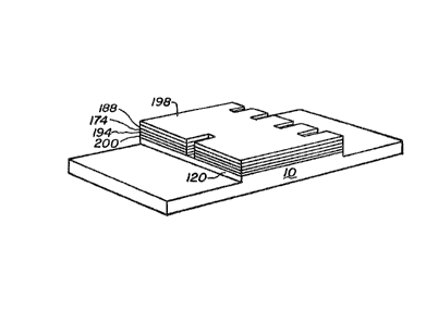
In thi~ ~o~ee~, a ~ubst~n~ally ~ry ~ho~o-
h~rd~ le ~llm l74 on two ~uh~t~ntlally d~Y ~ho~o-
h~rdenabl~ e~ 18yl~ ~ ~ g4 and ~00 ac~ l~minated on
ShQ ~tep 20 o~ t~e ped~tal l~.
Thi~ c~n be accom~ he~ by l~r~inat~t~g a tirst
~ur~a~e o~ b~e~ layer 200 to th~ sse~ ~o3 w~th a
~uppo~t ~mova~ly ~dh~re~ to a 8eOO21~ ~ur~aoe of Duf ~er
laysr 200. Th~ ~u~l?o~t 1~ then 2~0tr~d. a ~lr~
~ur~a~ o~ bU~ yox 194 i~ th~n 1alsinate~ on tho
~5 ~eooad our~c~ o~ bu~e~ l~y~ 200, w1th a suppo~t
remo~bly ;~lh~r~a to ~ ge~ond ~ur~ace o~ bu~f er layel
l94. The bufi~e~ lay~i:s 194 ~nd 200 a~e then har~e~ed by
~loodirlq ~hem with light o~ heating thera. ~ support
~8 ~emoved ~rom buff~ la~eE l9~ and. ~ 174 is
3~ îam~na~ed in i~ pla~e . Any ~pl; o~ o~ ~ilm 1~4 iB
~mo~ad. Then a ~a~k 134 1B lo~a~d on the f ~l~ 174 .
~he r~ask 134 hiving ~lea po~tion~ sub~tant~al}y
cozresp~nd~ ng ~co a ~ir~d ~hap~ o~ an optio~l ~aYeguid~
l58 and groov~s 142. The ~em~indo~ o~ the ma~ 4 i8
35 ~paque. ~he film 17~ ~ exl?s~ed to light th~ough th~
0l,as/s~ 14: 4E~ UPCINT LEGFIL NO. 010 017
~313~
~6
ma~ r ~ortions ~ol5~merizln~ a'c l~a~t one monome~ ln
~hR r~l~ 174 and ehangi~ ;hO r~raative ~ndax o~ ~h~
ex~o~a~ gllra tO ~o~m th~ ~tia~l wav~gul~e lS~.
Al~r~ v~ly, th~ X 13~ m~ ta~ on
5 t~o fllm 174, th~ R 174 ~olr~bly ~h~E~ t~ ~
~up~o~t . 'Irh~ ~ lm ~74 i~ then ~xp~d ~o li~h~ ~hrou~h
th~ ma~k ~ r ~o~tio~3. The tWQ bu~er 'l~y~r~ 194 and
~00 ~o ~h~ ninatQd on~o ~hQ ~tep 20 or gub~t~tut~d
~or th~ ~uppo~t on thQ f~ 174. If ~h~ ~orme~, thsn
u~or1: 1,4 ra~ove~ ~om th~ ~ilm 174 an~ ~he ~
lam'lnate~ on the hu~er l~ r 194. I~ ~he la~t~r, th~n
the bu~-r laye~r 200 18 lam~nated to t~ ~top 20. The
~u~er ~ 8 and ~llm are ha~denod by ~loodlrl~ with
l~ht or he~tlrlg at ~ome ~t~ge o~ th~ pro~a~s, bu~ th~
15 ;tllm ~ ~ ~aot har~ene~ b~o~ ~he w~v~uid~ i~ form~d.
~he w~ ui~a ~o~tlorl o4 the ~slc 134 ie then
~lock~ ~o p~v~rlt l~ght ~oln tran~m~ttlng~ th~rethrou~h~
~h~rl abl~civ~ raa~lon pro~rlde~ by ~ny
~ou~, 0uoh a~ xcim~r ~a~ae, ~ h ~n~y
20 ul~rav~ o~o~ h~ typ~lly at aso ~ om~e~r~
~;~veleJsgt!h, an lon o~ o~octron ~e~m, or ~che like, 1
di~ect~d orl the ~ool~ port~ on~ o~ t~ a~k 134 tO
d~ra~e tha i~m 774 an~ U~f~ layere lg4 an~ ~OC un~e~
~h~ cle~r ~oo~ ortl~n~ a~ ~h~ ~agk l~a ~n~ p~o~!lu~
25 ~u~ative ~ol~til~ comp~nen~ wh~h ex~t ~h~ ex~o~ed
~or~ion~ o~ the ~ yer~. In e~kee~, the expo~ed
~ilw ~n~ l~yer6 ar~ ~ubætan~i~lly ~t~hed or re~o~
Thi~ form~ groove~ 142 de~in~ by zeceilrin~ me2nR
pre~ ly a1igr~d w~t~4 the w~veguide l5a.
3~ ~h~ ms~J~ 150 i~ remD~ed. Tw~ more ~u~er
l~yer~ LBB ~nd 1~ are lamin~ted onSo the f ilm 174 an~
~hen hard~r~ed . ~h~ ma~k 15~ la2e~ onto b~f f ~r l~ye~
~9~ allg~niAg ~he cle~ groove po~tlorl~ over ~he ~ooYes
already re~o~ or otohe~ ou~. ~lduoiary 7~ark~ ~an ~e
3~ ~e~ on ~he ~a~c 15~, ~llm 174 ~nd lare~s ~9~ and ~o~ to
4t~ 811~R
~'
01i05~ 1 14:41 DUPONT LEG~L NO. 010 018
:L3~3~37~
17
I'c 102y ~e aav~nt~eou~ to ~B~ ~ ~lightly
er~nt ma~k tO remove ~rnov~ ~ortion~ ~om buf~e~
~ayer~ 188 a~d 1~. U~ns ~ ma~k on ~uf~3r lay~rK 188
and 19~ w~th ~a~ gEOOV~ ~ort~on~ htly wi~@r than
5 ~he cl~ oo~ o~tior.s u~d on ~ 74 ~r~d ~uf f er
lay~ 200 will ~aoil~ta~ ~oaSt~oning o~ ~he
groo~e ~o~t~on~ ~tl bu~fo~ layer~ l~a an~ ~a entt ~ly
ov~ g~ooYe portion~ ~ret~iou~ly Pormed in ~he ~ilm
174 arld bU~r 1~Y~EO ~94 ~nd 200.
~ Th~ ~u~r Llly~lPill lBa ~nd ~98 ~re ~hen
irr~dia~ed ~hrouqh tha ~1l3ar ~EOOV~a ~Or~ ~n~ O~ th~ ~Qd~k
lS~ by th~ ab~tlv~ r~di~eiOrl 202 ~UbÇ'~antia11Y remOVing
th~ bu~er l~ a ~ a~d ~g~ ~nd~ he ~1e~ ~rOOYe
POrt~On~ O~ the m~k 15~ n~ ~OOVe6 de~nea ~Y
a~ r~C~ ng m~an~. In th1~ ~6a~1Y, ~h~ 1ng
S 0 inte~ra1 W1th ~he OPti~a1 WaVe~Ui~e a~Y1C~ .
O~t~C~ 4fi ~n~ ~O~ r 6~ a~ ~4ai~iOr~d
a8 ~e~1bed 1n re~ran~ to ~1gUr~ 6. Y1~B o~n b~
~orm~ to optlcally ~orm~ th~ optlcal f ~ a~e~ an~
Z th~ wav~ id~ ~ p~çv~u~ly ~e~ d.
Alternae~l~sly~ bU~E l~y~re 1~ and 198 can
R~ Rt~ O~ltO a aov~ 160. M~01t 158 or ~ m~ ~ith
lt~y lar~r ~lea~ 9roove po~ n~ i ~ t~ amirlat~d
~o t~e ~r~e ~ur~a¢0 o~ her ~tlf~r la~r~r 1~8 or 198
2S fartt~est from ~h~ cov~c l~0. ~he ~oov~ porclon~ o~
bu~fer layeræ 188 and 198 are t~rl sub6t~,ntially etr~hed
ou~: as abo~re des~ ed . ~hen th~ buf ~e~ layers 188 ~nd
1~ are h~r~en~. The rQ~ then ~e~nGved. Op~ical
~iber~ ~6 a~e poe1tione~ aTld ~ecured. in $he p~tl~l
3~ rec~ivir~g ~ea~ on ~h~ ~ede~al 1~0 o~ oov4~ 160. ~hen
th~ LQ~alnlng part. i.e., the oov~ lS0 o~ ~ede~tal
1~ conne~ted, ~uch that the c~ lng ~Pe~n~ on the
~8estal 110 ~nd the reoeiv~ing r~ean~ on the oo~er
enoloss ~h~ cla4~ng~ ~ ehe opt~ oal ~tber~ .
~ .
17
01~135/8~ 14: 41 DUPONT LEG~L NO. 010 019
-
13~3~7~
1~
The ~ mbl~r llluo~rAted ~n Pi~ur~ 12 C~ ~18C
be m~de by remo~ ooYe portlon~ ~rom the fl~ ~74
a~a bu~f~r lay~ 200, 19~ nd 19~ b~r oh~cally
w~h1 n~ ~h~ out sim~l~r to a~ pr~viou31y d~cr~be~ ~ith
r2~ ct ~o Flgu~ nd 5 .
~ p~ol~ ~ally, ,~ m~c ~ laminat~ on a ~rRt
p~o~oha~don~ble bu~e~ lay~r on a ~ho~oh~den~bl0 tilm
h~v~ an o~tlc~l wa~regulde on a ~cond pho~oha~aenab~e
bu~ ~r lay~ on ~ pe~ta~. ~he masl~ 1~ ad~t~a ~o
lo blo~k a~nio ~ h th20ugh area6 ~orre~onaing to
~oove~ to ~ ~o~ the ~ilm an~ ~ay~r~ for
re~elvlr~ o~t~&~l i~e~ c1~dd~n~rs an~ ~or~s. ThQ ma61c
le 41~0 ~da~te~ to tran~mit ac~in~c r~stion ~h~ough
ar~ co~re~po~dln~ to a desl~d wave~ui~e tevle~
nclu~ng ~h~ wa~egu~e and means ~inin~ tt~e ~roove~.
Tho ~ an~ ldyers are ~looded with bro~d band
ul~ravlolet l~h~ ., actlnic ra~i~tion, ~hrou~ t~e
~a~X. ~hl~ har~n~ the ~ Q an~ laye~G~ The maelc 18
~mo~ hen the un~lood~ reg~on6 o~ th~ na
2~ l~yg~ a~e ~e~w2d ~y wa~2~ing w~th arl appropri~t~
sol~ren~, An o~ a~ f iber ~onn~tor a~ bly Pe~lu~t~
hs~rln~ ~n o~ieal wav~guid~ deviae ~n~ral ~rith mean3
~f~ groo re~ fo~ reoelving cla~din~s ~na ~o~e~ o
o~tl~a~ ~b~ro.
2fi As with previou~ly des~ribed a~6emblies. a
~ore an~ ~laddin~ of an optl~al ~iber ~n be pla~ea 1~
the g~ooYe~ whlle il~c~cet8 O~ e o~ti~al ~ib~rs ~re ~et
on pede~tal 6urEaCe~ ad~acent two end~ of ~he p~de~al.
All p~r~o of ~e a~xem~ly or a~emblle~ D~ the
30 presen~ vention can bo bond@d or ~e~led with a
h~rdened ph~tap41ym~r. ~ar~ ~atl b~ encloeed ~rora the
envlronlue~t by hacdene~ pt~o~opolymer or o~he~ ma~e~ial
~U4, suoh aa epoxr. Th~ ~an ~e accom21ish~d ~y dipping
ths as~embly with o~ wl~hout a ~OV2~ 'I n a ~uita~le
3~ cura~le llquid. ~e Fi~u~ 13.
.
.
01i05/f39 14: 42 DUPI:INT LE[iflL NO. 010 020
~.
~3~3~
1~
Tho~ ~kllled ~n ~h~ a~c, h~v~ ng the ~et3e~le
o~ the t~hin~f~ o~ ~n~ ~re~Qnt l~ t~ on ~ he~ na~ov~
s~t ~orth, ~an ef~ num~ou~ modl~c~tion~ th~3to.
~h~ modli~lc~t~o~ ~re ~o b~ aorll3t~ue~ b~lng
en~ompa~6~d wi~hin the ~c0~3 o~ 1:h~ pro~ t ~rentlo~ a~
~e ~ort~ ln the app~nded ~ m~ .
., 1
~5
3t~
: 1
,~