Note: Descriptions are shown in the official language in which they were submitted.
- ~ 3 1 327~
BC988-005
CONTROL OF PI3?ELlNED OPERATION IN A
MICROCOMPUTE~ SYSTEM EMPLOYING DY~AIvIIC BIJS SIZING
WI TE 8 0 3 ~ 6 ERO CESS OR Ah-D 823~5 CACh2 CONTROLLER
~ESCRIPTION
Technical Fieid
The present invention relates to improvements in
microcomputer systems, pariicularly microcomputer
: systems which empioy dynamic bus sizing and pipelined
operations, and more particularly in such systems
wnich further inciude a cache subsys~em.
Background Art
Background information respectin~ ihe P0;86, its
characteristics and its use in microcomputer systems
including cacne memory subsystems ar2 des~ribed in
Inte;~'s "Introduction to the 8G38~", April 1986 and
tne ~,0386 Hardware Reference Evlanual (1986). Tne
characteristics and operating performance or ihe
82385 are described in the Intel publication "82385
High Perrormance 32-Bit Cache Controller" (1387)o
In microcomputer systems, as in other computer
systems, speed of operations is an importan~
criterion which in most cases has to be balanced
against system cost. Many reatures whicn were first
introduced to speed up operations in mainframe
computers and minicomputers are now finding their way
1 3 1 3274
BC988-005
into microcomputer systems. These include cache
memory subsystems and pipeii~ed operations.
In some microcomputer systems (for example those
employing the Intel 80386), pipelined operations are
an attractive operating option. For 80386i82385
microcomputer systems the 823&5 cache controller
provides an NA signal which it is suggested should be
connected to a corresponding input on the 80386.
This ailows the 82385 to assert the N-A signal to the
80386 prior to completion of a given bus cycle to
enable the 80386 to outpu~ information (data, address
; andjor control) for the next operating cycle. Tne
timing is arranged, along with connected components,
- so that if a cache operation is the given operation,
information for the given operation Aas alreaay been
accepted by the cache memory and therefore changing
the 80386 output information to correspond to the
next cycie will not interfere wiih tne operation
which is in the process of being completed. This
also hoids true for situations in wnicn a cache miss
condition has occurred requiring rererence nol to the
cache memory but to main memory since access to main
memory is via latched bufrers which tnerefore store
information respecting the glven operation.
2~ The 8G386 aiso has the capability or operatin~ with
wnat is referred to as dynamic bus sizing. The
80386 is nominally a 32-bit machine, i.e. tne width
of the data bus is 32 bits. However, tne 80386 can
operate with 16-bit devices (devices which wili
transfer oniy î6 bits or data) by responding to a
1313274
BC988-û05
~16 signai which is provided to tne 80386 to
indicate tne presence of a i~-bit device. The ~Si6
signai is important to tne 8Q386 in the event that it
- has perrormed a 32-bit opera~ion. Of course ~he i~-
bit device cannot, in one operalion, transfer tAe 32
bits of data whicn the 80386 is capable or generating
and/or accepting. Thus, a second operation (cycle~
is necessary and the 80386 responds to the BS16
signai to automatically generate the nex~, necessary,
cycie.
In order for this type or operation to oe successrui
when tne 82385 is present it is also necessary for
the 8238~ to have in~ormation respec~ing ~he
character of the device taking part in the operation
i5 so tnat the NA signal to the 80386 is not
improvidentiy generated. As descri~ed in the
rererenced Intel publications the 82385 requires
device informalion at tne beginning of a cycle in
contrast to the 80386 which can accept and act on
2û device informalion substanlially laler in the cycle.
In some microcomputer systems, this constraint is
accepted by correiating the ada~ess of a device witn
its size so that for exampie all 32-bit devices are
in a first predetermined address range and ail 16-bit
devices are in a second, different address range. By
tnis technique then, the size of a device can be
determined by its address.
However, in systems which require the fiexibility of
iocating a wide variety of devices witnin widely
1 3 1 3274
BC98~3-ûû5
varying address ranges, tnis consiraint cannot be
compiied with One class of sucn systems are those
employing the IBLVI Micro-Channel (TM) bus.
In many systems, including systems or the roregoing
5 type, a device when addressed will return an
indication or its size. However, since the 82385
requires device size inrormation lo be available at
the beginning or a bus cycle, in systems where this
information is only available later in the cycle,
i0 there is the possibility or an improvident NA signal.
Therefore it is an object or the present invention to
proviae an arrangement in an 80386i82385
microcomputer system which selec~ively controls the
NA signai so that it is coupled to the 8û386 only
under appropriate circumstances. In oiher
circwmstances the NA signal is prevented rom
reaching tne 80386. Preventing the NA signai ~rom
reaching tne 80386 prevents pipelined operation, i.e.
it prevents the generation or inrormation ror a next
2û cycle berore t~e given cycle has been completed.
With this flexible controi or the NA signal, the
microcomputer system can now operate with dynamic ~us
sizing, i.e. it can now operate with devices of
various sizes without information at the beginning or
the cycle as to the size or the device being operated
with.
Cacheabie devices, i.e. devices generating data which
can be cached~ are necessarily 32-bit devices. All
sucn devices nave addresses (specifically, tags)
1 3 1 3274
BC988-0û5
indicating cacheability. Ail other devices (whether
or no~ 32-bit devices) have addresses indicating
inrormation they generate wiil not be round in cache.
~ontroi of the NA signai depends in part on
cacheaDility. Specifically, since any cacheable
device is a 3~-bit device, there is no question of
improvident NA signals when operating with cacheable
devices. Furthermore, in the event of a cache hit,
there is no question but that the NA signal is
appropriate since only cacheable devices (32-bit
devicesj will produce a cache hit. Thus an important
feature or allowing dynamic bus sizing and pipelined
opera~ions is preventing or inhibiting the NA signal
from reacning tne 80386 in the event or asseriion of
an address to a non cacneabie device.
If, during the course or a given cycle (where the NA
signal has been inhibitec.), it turns out the device
is a 32-bit device, then the cycie completes in
normai fashion (without pipeiiningj. On the other
2G hand, if it turns out during tne course of the cycie
that the device being.operated with is a 16-bit
device (and the cycle is a 32-bit cycle), then the
80386 generates the additional, necessary cycle.
This operation is encirely transparent to the 82385,
i.e. the 82385 takes no part in controlling the
second of the two cycles. Finai~y~ if the device
being operated withn turns out to be an 8-Dit devlce,
then the 80386 "sees" a 16-bit device so that it
operates exactly as nas been described for tne case
when the device is a 16-bit device. In otner words,
the 8G3&6 "sees" a 16-bit device so that arter the
1 3 1 327~
BC988-OG;
rirst cycle is completed ~during which cycie ii is
inrormed that it is operating with a 16-bi~ devicej,
a second cycle is generated. ~owever, not oniy
transparent to the 82385, but alsa transparent to the
8~386, other logic converts each of the i6-bit cycles
or the 80386 into two 8-bit cycles. Thus in the case
where a 32-bit cycle is directed at an 8-bit device,
the 82385 takes no part in the operation, the 80386
generates two 16-bit cycies, and other logic operates
on each of the 80386 16-bit cycles io generate two 8-
bit cycles.
Thus in accordance with one aspect, the invention
provides a microcomputer system with pipeiined
ins~ruction sequencing responsive to a nex~ address
signal prior to completion or a pending operation,
said microcompuier system comprising:
a processor of a given bit widtn,
a cacne memory subsystem of said given bit widtn
coupled to said processor by a iocal bus,
a rurther bus connecting said local bus with other
; components having said given bit width and with at
ieast one component of a reduced bit width, at ieast
some or said components having said given bit width
having an address in an address range associated with
said cache subsystem and said at least one component
of reduced bit width having an address outside an
address range associated with said cache subsystem,
wherein said microcomputer system rurther includes:
' -
131327~
BC588-005
a~ address decoder means responsive ~o an asserled
address on said local bus ror generating a signai
indicating whether said asserted address is or is not
within said address range associated witn said cache
memory subsystem, and
b) iogic means responsive to said signal rrom said
address decoder means ror generating a next address
signal to said microprocessor ror pipelined operation
uniess said address decoder means indicates an
iû asserted address outside a range associated with said
cache subsystem.
~rier Description or the Drawings
Fig. 1 is an overail three-dimensionai view or a
~ypical microcomputer system employing the present
invention;
, . . .
Fig. 2 is a detailed block diag.-am of a majority of
tne components or a typical microcomputer system
employing the present invention;
. .
Fig. 3 is a block diagram, in somewhat more detail
2û than Fig. 2, showing those connections between the
8û386 and 82385 recor~mended by the manufacturer and
which is useful to an understanding of why such an
arrangement is inconsistent with dynamic bus sizing;
Fig. 4 is a more detailed block diagram similar to
Fig. 3 but illustralin~ application OL the present
1 3 1 327~
BC988-005
invention whicn aliows both pipelined instruction
sequencing and dynamic bus sizing;
~ig. 5 is fur~her detailed block diagram of apparatus
which handles 16-to-8-bit cycle conversion
transpareni to both the 82385 and 80386; and
Figs. 6 and 7 are a timing diagram and a block
diagram of the latch DL and its control signal LEDc
~Latch Enable from Drv~) to iliustraie how ~he
synchronous DlV~ subsystem is interraced to the CPU
local bus (operating under a difrerent clock) to
avoid possible contention on the system bus 25û.
Detailed Description or a Preferred Embodiment
Fig. 1 snows a ty?ical microcomputer system in which
the present invention can be employed. As shown, the
microcomputer system lG comprises a number of
components which are inlerconnected together. More
particularly, a system unil 30 is coupied to and
drives a monitor 20 (such as a conventionai video
display). Tne system unit 30 is aiso coupied to
input devices such as a keyboard ~0 and a mouse 50.
An output device such as a printer 60 can also be
connected to the system unit 30. Finaily~ the system
unit 30 may include one or more disk drives, such as
the disk drive 70. As will be described below, the
system unit 3û responds to input devices such as the
keyboard ~iû and tne mouse 50, and input/outpu~
devices such as the disk drive 70 for providing
signals to drive output aevices such as the monitor
.
-
1313274
BC988-û05
20 and the printer 60. of course, ~hose s~ilied in
the art are aware that otner and conventional
components can also be connec~ed to the system unit
; 30 for interaction therewith. ln accordance with tne
present invention, the microcomputer system iO
includes (as wiil be more particulariy described
below) a cache memory subsystem such tha~ there is a
CPU local bus interconnecting a processor, a cache
control and a cache memory which itself is coupled
via a buffer to a system bus. The system bus is
interconnected to and interacis with the I/O devices
such as the keyboard 40, mouse 50, disk drive 70,
monitor 20 and printer 6û. Furlhermore, in
accordance with the present invention, the system
i5 unit 30 may aiso inciude a third DUS comprising a
Micro Channel (FrI) architecture for interconnection
beiween the system rus and otner inputjoutput
aevices.
, . .
Fig. 2 is a high ievel block diagram illustratiny tne
various components of a typical microcomputer system
in accordance with the present invention. A CPU
local bus 230 ~comprising data, aQdress and control
components) provides for the connection of a
microprocessor 225 (such as an 80386i, a cache
control 260 (whicn may include an 82385 cache
controiler) and a random access cache memory 255.
Also coupied on the CPU locai bus 230 is a bufrer
240. Tne buffer 2~G is itselr connected to the
system bus 250, also comprising address, data and
control components. The s~stem bus 250 extends
oetween the buffer 240 and a further buffer 253.
~31327~
BC988-005
îG
The system bus 25G is aiso connected to a bus
controi and timing eiement 265 and a DMA controlier
325. An arbitration eontrol bus 34G coupies the bus
control and timing element 265 and a centrai
arbitration element 335. The main memory 350 is aiso
conneeted to the system bus 250. The main memory
includes a memory eontrol element 351, an address
multiplexer 352 and a data burrer 353. These
elements are intereonneeted with memory elements 3~0
lG through 364, as shown in Fig. 2.
A rurther burrer 2~ is coupled between rhe system
bus 2iO and a pianar bus 270. The planar bus 270
includes address, data and control components,
respectively. Coupied along the planar ous 270 are a
variety or I/O adaptors and other components such as
the dispiay adaptor 275 (which is used to drive the
monitor 20j, a clock 280, additionai random access
memory 285, an RS 232 adaptor 290 (used for serlal
I/O operations!, a printer adaptor 295 (which can be
2G used to drive the printer 60), a timer 30û, a
diskette adapior 305 (whicn cooperates with the disk
drive 70), an interrupt controiler 3iO and read only
memory 315.
The burrer 253 (coupled on one side to tne system bus
25G) is coupled on tne other side to the Micro-
Channel (TM) sockets ~01 of the Micro-~hannel ~IvI)
bus 320. Bus 32û can support devices or various size
including 32-bit devices, 16-bit devices and 8 bit
devices. A typicai memory device 331 is shown
1313274
BC98~s-ûû5
coupled on Ihe bus 32û. One of the advan~ages of
tnis bus LS tne rlexibility the user is provided with
to freeiy insert various devices in the àirferent
sockets, at will. The mixing or these devices and
their appearance ai difrerent sockets prevents rigid
addressing allocation and is a prime reason for the
necessity or the present invention. Absent tne
present invention, the 80386i82385 microcomputer
system as descrlbed herein would be either wholly
prevented rrom using pipelining operations or
alternativeiy subjected to fauity operation caused by
improvident or inappropriate pipeiining operations.
Fig. 3 shows selected interconnections between the
8038~ and 32385, reiative to generation and use or
the Nexl Address (NA) signai, as recommenced by ~he
manuracturer. More particularly, the interrace
between the CPU locai bus 230 and the system bus 25û
is the burrer 2~0 whose components include a control
burfer DL (ror data) and AL (for addressj. As shown
in Eig. 3, the data component of the CPU local bus
(CPULBD) is one inputioulput connection for the DL,
on the CPU iocal bus side. Likewise, the data
component SBD or the system iocal bus 25û is the
inputioutput conneciion to tne DL, on the side or the
system bus 250. The burfer DL is controlied by iis
input signals LDST~, BTjR and DOE. LDSTB latches
data into DL and DOE enables the output or DL, The
direction rrom which input is accepted (CPU local bus
230 or system bus 250) and to which output is
directed (system bus 250 or CPU local bus 230) is
determined by BTjR.
~ `~
13~3274
~988~a05
Likewise, the address componenc or the burrer AL has
an input from the address component or the CPU iocal
bus ~CPULBA) and an output to the address component
or the system local bus 25û (SBA). In a slmiiar
fashion, tne AL component of the bur~er is controlied
by its two control signals BACP and BAOE, the rormer
latches address information from CPULBA into AL and
the latter enables che output, i.e. so the system bus
25G. The control signals LDSTB, DOE, BACP and BAGE
are provided for by the 82385.
; The address component CPULBA or the ~PU iocal bus 230
origina~es at the 80386 and the data componeni CPULBD
of the CPU local bus 23û originates/terminates at
the 803~6.
The 82385 uses two additionai siqnals X16 and NCA in
the generation or the NA signal. Tne X16 signal
indicates whether the device which is being operated
wi~h is a i6-Dit or 32-bit device. one source or
the signal Xî6 is the Local Bus Address Decoder
2û ~LBAD). In addition, the manuracturer recommends
that the signal ~S16 be tied to the signal Xi6. The
signal BS16 is input to tne 8û386 to indicate to the
80386 wnether Ihe device being operated with is i6 or
32 bits in size. A source or tne signal BS16 is a
device address decoder, such as MAD~ MAD represents
the address decoder or any device coupled to the
s~stem bus 250 or any other bus coupled thereto such
as the bus 270 or 320. When a device such as MAD
recognizes its address on a bus address component
. .
1 3 1 3274
BC988-ûû::~
such as MA, lt returns the signai BS16, which is high
or low depending on whether the device is a i6- or
32-bit device.
The Non-Cacheable Address (~-CA) is another input to
tne 823&5 which indicates whether an address asserted
is a cacheable address. A cacheable address is
defined as an address for a device which is
compatible with the cache subsystem and hence i5 a
32-bit device. This signai is generated by the Cache
lû Address Decoder (CAD) by virtue or an input from the
address component of the CPU iocai bus 230. The
manufacturer suggests that a portion of memory can be
set aside as non-cacheab~e by use or this input to
the 82385.
The recommended architecture illustrated in Fig. 3
provides ror effective pipelined operalions (by use
of the NA signal) under any one of the roilowing
circumstances:
1) where all devices connected io the system bus 250
or any bus coupled thereto are 32-bit devices, or
2) where the devices connected to the s~stem bus 250
or any bus coupied thereto may be 32-bit or i6-bit
devices, so long as the signai X16 is avaiiabie at
the beginning of any bus cycle.
When the X16 signal is available at the beginning of
a given bus cycle, the 82385 based on that
information determines whether the NA signal is
1 3 ~ 3274
BC988-û05
1~
appropriaie, and if it is not appropriate, it is not
generated. ~hus in the event the 8û38~ is operating
with a 32-bit device, then the NA signai is normaiiy
generated prior to completion of a given cycie for
erfectiny pipelined operation. On the other hand, if
the device is a 16-bit device, then the NA signal is
not generated, allowing the 8û386 to generate the
second necessary cycle for proper operation with a
i6-bit device.
lG However, the architecture or some bus subsystems (fox
exampie the Micro-Channel (TM) busj provides ror the
mixing of 8-bit and i6-bit and 32-bit devices.
Because tne signal Bsl6 is not returned until
sometime arter the t~pical device MAD has recognized
its address on the bus subsystem, it is not gcnerated
early enough for the 82385 to take into account iIl
determining whether to generate NA. Acccrdingly, the
peculiarities or the 82385 make it incompatible,
particularly in the generation of tne NA sigrlai, with
2G bus subsystems having the flexibility such as is
e~hibited by the Micro-Channel (TM) bus.
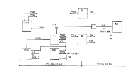
Fig. 4 is a block diagram similar~to Fig. 3 but
altered ror use in accordance with the present
invention. Berore describing the operation of the
apparatus shown in FigO ~, a number of the
differences between Figs. 3 and ~ will be described.
One major difference is that tne outputs Xi6 and NA
rrcm the 82385 are no longer utilized.
1313274
~C383-Oû5
In addition, a new logic element CLI is interposed
between the 8238~ and the 8û386. Tne iogic eiement
CL generates the CEUNA signal (repiacing the unused
NA signai rrom the 82385). Tne logic unit CL iS
responsive to the NCA signal rrom the CADR and BADS
signal from the 82385 (indicating whether there is a-
cache miss~ The iogic element CL also has an input
~W/R indicating whether any system bus cycle is a
read or a write. As will be described, whiie BW~R
lû is used in an embodiment or the invention, it is a
signal which is not essential.
The decoder CADR receives, in addition to its inputs
from bits A17-A26 and A31 of the CPUL~A, Programmable
Cacheability Bits (PCB). In an embodiment actuaiiy
constructed, the rirst or ihese three biis repres~nts
a decision to ailow caching ROM space. ~, second bit
either enables the decoder CADR tO OUtPUt NCA based
on the decoded information, or altexnatLvel~r, ~o
declare ~ll accesses non-cacneabie, i.e. assert h-CA
2G regardless or the asserted adaress on the C~ULBA.
Finaliy, ~ third bit indicates, in one state, that
address space between û and 8 megabytes is cacheable
and that address space between 8 ~o i6 megabytes is
non-cacheable. In the other state, the bit indicates
that address space in tne range O to i6 megabytes is
all cacheable. If desired, ihe erfect OI this bit
can be multiplied by simply reflecting the status of
the rirst î6 megabytes through the succeeding 16
megabyte ranges. Of course, the use of these
particular cacheability indicators (or otners~ is not
essential to the invention. It is, however,
1 3 1 327~
~C388-005
1~
important to arrange the CA~R so that it can quickly
decode its inputs and produce h-CA. 'n an embodiment
actuaily constructed, the timing window ror
production of NCA, from vaiid addresses on the
CPULBA, was very short, on the order of ten
nanoseconds.
A further major dirference between ~igs. 3 and ~ i5
that the t~pical MAD now generates nol a single BSi~
signai (as is the case in Fig. 3), but ~o signals,
CS32 and CSl6. This enables the MAD to identify
itselr as a 32-bit device, a 16-bit device or an 8-
bit device. Tne signal CS32 is input to a flip-flop
FF which is now used to generaie the BS16 signal
- which is in one condition in rhe event the M~D is a
32-device and in a different condition if the Ivl~D is
an 8-bit or a 16-bit device. Ir neither CS32 or ~S16
is generated by the device, then by default the
device is an 8-bit device.
The iogic equations which have been referenced above
are reproduced immediateiy below. In this materiai
the symbols have the foiiowing meanings associated
witn them:
J
Svmboi Definition
i Negation
= A registered term, equai to
= A combinatorial term, equal to
& Logical AN-D
+ Logicai uR
1 3 1 327~
r~
S
r~J r~
~ :r
rr. ~D, r
R~ r~
O ~S ~
U
r ~
_
r~
rn r~
r~ Q 3 rJ
,~
~,
O ~ rn ~
QIn ~ ~,
t~ IS L~
rn r~
~n rn ~ Q
r~ R~ Q ~ ~S
u Ln l q n r~ ~ In
~ r.~ ~ 3 X r7~ 'Y
r~ rm rJ rJ rJ
~ ~ r~ m t>~
~ m u ~
r~rf~ p~ Q ~) ,~ ~ .
r~1~ `~ r~ n In
~ m ~, m `~ m ' ' u u
r h rn ~ ~ ~ r rn rr.
` ~ + + + + ` + + + +
Ln O
1~
~313274
n
r~
1'~
r~
~ 1
,~ r~
r
m
r~ ,5 X
r~
zi r~
_ ~ 1~ ;~
n ~ ,~
;~ m r~
r ~ ~ ~ oo
r~ r~ r~
~ rn r~
r~ n
~n ,5 r~
x )~ m ^ rn ~
u m ~ r ~ r~
u rn r~
r
,~ r~
r
~5 r~ r~
z; m ~¢
r~
r~ In
r~ ~ z r~
~n l~
,5 ,:~ Q .~ rJ ~ r~ -
z r~
n u In r~ rr~
~ m ~ ~ co r~ H r~
~ rn r~ ~ r ~ H ~S
rn ~ r~ ~ ~
rn ~ rJ ~ r~ ~ ll In
rn ~ ~ ~ r~ ~ rn m ~ rq .. In r
rn ~ In r r~
r
~ rn Zi Z; Z Z - ~ rn r
~ rn :~ ~ ~ ~ ~ rn rn rn r~ r~ P~
Z H P~ u~ rn H H 1~ P. H
) V r~ rn H ~
:~ ` + ~ + + + ` + + + `` ~ +
In O
/~ .
1 3 1 3274
BC988-GG5
In the roregolng logic eq~ations the roliowing
signais are described or referred to in tne ci~ed
lntel puDlications:
BADS
~R~ADY
(BWjR) actualiy rererred to as BWiR, the
parenthesis are used to indicaie that the
entire term is one signal
CLK
0 (WjR) actualiy rererred to as W/R, the
parenthesis are used to indicate the
entire term is one signal
F~A~S, when active indicates a valid address on the
system bus 250. BREA~-Y is a ready signal rrom the
sysr~m bus 25G to tne CPU local bus 23G. BW/R derines
a system bus 250 Write or Read. CLK is a processor
clocking signal which is in phase with tne processor
225. (W/R~ is the conventionai Write or Read signai
ror the CPU iocai bus 23u.
Equations (i)-(5) derine:
BT2
BUSCYC385
CE-u~-A
MISSl
PIEEC-YC385
in terms or the derined signals, the signals
described or rererred to in the cited Intel
publications and NCA and NACACHE.
1 3 1 3274
~C98~-~05
~T2 refiects the state of the system DU~ 25û. The
state BT2 is a state defined in the cited lntei
pubiicationsO
BUSCYC38; also reflects the state or the system bus ~
250. It is high for bus states BTI, BTl, BTïP and low
for bus states B~2, BT2P and BT2I (again these are
DUS states referenced in the cited lntel
publicationsj.
CPUNA is a signal to ~he 80386 ailowing pipeiined
iû operation. This is the signal which replaces the NA
signai from the 82385.
MISSl is active defining the first cycle in a double
cycle for handling 64 bii read to cacneable devices.
PIPECYC385 is active during BTlP (wnich is a bus
state referred to in the cited Intel publications.
NCA is a signal created y decoding the address
component on the CPU locai bus 23u to refiect, ~hen
active, a non-cacheabie access. Cacheability is
determined by a tag componenl (A31 to A17) and
programmabie information definin~ what ta~s (if any;
refer to cacheable as opposed to non-cacheable
addresses.
NACACHE is a sign~i simiiar to ihe BNA signai. ~NA is
a system ~enerated signal requesting a ne~t address
from the CEU locai bus 230, and is referenced in the
1313274
sc988-oOS
cited Intel publications. NACACHE differs from BNA
only in respect of the fact that BNA is created for
32K cache while NACACHE is created for a 64K cache.
so long as the cache memory is 32K, as cited in the
Intel publications the ~ACACHE signal referred to
here could be replaced by the BNA signal.
Reviewing Equation 3, the set terms are found in
lines 1 and 2. The term on line 1 indicates a
pipelined operation. /MISS1 indicates a 32-bit
operation (as will be described) and so CPUNA is
appropriate. The term on line 2 is a cycle that ends
early without pipelining, e.g. /BREADY. Referring to
Equation 4, the terms on lines 1 and 2 are the set
terms. Both depend on NCA.
Fig. 5 is a detail of apparatus associated with the
buffer and decoder 254 (associated with bus 270) and
buffer 253 (associated with a Micro-Channel (T~) bus
320). As has already been ~escribed, the apparatus
of Fig. 4 provides for two 1~-bit cycles when 32-bit
cycles are directed to 8- or 16-bit devices, and does
so in a manner transparent to the 82385. The
apparatus of Fig. 5 is employed so as to generate,
for each 16-bit cycle directed to~an 8~bit device,
two 8-bit cycles, in a manner which is transparent to
the 80386.
More particularly, the apparatus includes control
logic CLA, a sequencer S and a controlled coupler ALS
which couples selective ones of the data lines to
others of the data lines. Mor~ particularly, as
1 3 1 327~
BC988-005
22
shown in Fig. 5, the low order eight bits (D0-D7)
can be coupled to the second 8-bit segment (D8-D15)
under the control of the signal DIR and ~G. Further,
the direction of transfer (left to right or vice
versa) is also controlled by DIR.
More particularly, in any 16-bit cycle generated by
the 80386, data is placed on the low order sixteen
bits of the data bus. In order to convert a 16-bit
cycle generated by the 80386 into two 8-bit cycles
for the appropriate MAD, the hardware shown in Fig. 5
forces the 16-bit operation to look like two 8-bit
operations to the 8-bit device MAD while to the 80386
the two 8-bit cycles look like a single 16-bit cycle.
The control logic CLA performs a decode function for
the conilersion cycle control. It detects when a
conversion cycle must occur and controls the GAT~ 245
and DIR 245 signals of the ALS which connect the low
order eight bits of the data bus to a second 8-bit
segment of the data bus. The logic equations for CLA
are listed below. Once the conversion cycle
conditions have been detected, the signal DATACONV
activates the sequence. The signa1 CS16, when
inactive, signals presence of an 8-bit device and
hence the necessity for the conversion. The signal
CS16, when active, indicates a 16- or 32-bit device~
Q1 is used in the sequence to indicate the end of the
first half of the conversion cycle. The signals
DATACONV and Q1 are input to the sequencer S. Tne
sequencer S performs two functions. One is to hold
30 the 80386 not ready until the second half of the
131327~
BC988-005
cycle has been initiated. ARDYEN is driven to a
logic 1 to signal the 803~6 not to end the cycle.
The seque'ncer also stimulates the end o~ one 8-bit
cycle and the beginning of a second. ALTALE clocks a
logic 1 onto the AO address line and causes the wait
state generator to restart. CMTLOFF causes the
active command signal to go inactive and active again
to stimulate the end of one cycle and the beginning
of another. CONVAO is used as an input to the AO
address latch to force AO to a logic l for the second
half of the conversion cycle.
The completed 16- to 8-bit conversion cycle is
equivalent in time and function to two consecutive 8-
bit cycles.
The signais referred to above and shown in Fig. 5 are
defined as follows:
-- MEMCS16 16 bit memory device select
~I/OCS16) 16 bit I/O device select. Part~nthesis
are used to indicate the expression
relates to a single signal
AENl, AEN2 Address enables from D~A controllers
MEMR,MEM~, IOR,IOW CPU command signals
XBHE Bus high enable, indicates when data
should appear on a higher order eight
bit segment of the data bus
1 3 1 3274
~C988-005
24
XA0 Least significant address order line
Ql Wait state generator output (2d state
output)
-
D0-D7 Lowest order eight bit segment of the
data bus
D8-D15 Second eight bit segment of the data
bus
ARDYEN Asynchronous ready enable to 82284
[?]. ADDS wait states in conversion
cycle to provide for the generation of
two 8 bit cycles.
ALT ALE(active high) Alternate address latch.
User to clock A0 to a logic
-- on~ and to restar~ the wait
sta~e generator for second 8
bit transfer
CONV.A0 (active high) Conversion cycle A0.
Provides a logic one to the
A0 address latch so that A0
~0 will increment for the
second 8 bit cycle
CNTLOFF Control off. Turns off the active
command signal for 3 clocks ~?] to
simulate the end of one 8 bit cycle
1 3 1 3274
BC9-88-005
and the start of the second 8 bit
cycle. CNTLOFF is also used to latch
the low order data bus to the CPU
(during a read cycle~ on the first 8
bit transfer. Input to the 82288.
+ + + t, + ~ t,` + + + + + ~, 131327~
ô o (~ D ~; Z; N~ ~ H H tri 1-3
n ~ u~ u i~,
U~ U H 0 ~ ~-U~ U~
D' D~ Z 3 Z~ 3 D' D Z
Dj ~ ' ~ t ~ trl t J, ~' ~'tDi ~J Z
N ~ ~ Z H 3~ tl~ t~l
R'7 ~ ~ O tr~ R7 ~ ~
3i. ~ ~ trj
~i i-i ~' D~ ~ ~ H 1-1 ~ D'
z ~ i O O:~' t i O
~' ~ 3. ~ N ~
10 R') ~ .
10 ~
!`. tr~
t J ~ X trl tri ~:
tII t r ~ ~, X D' O
trJ trJ 1O D~ D' O ~j u
~ ~ ~.
~i ~i D~ `~ t~ri
O t~
trJ D
R~
~,
D
?
1 3 1 3274
~C988-005
~ Fig. 7 shows a detail of the latch DL, the data
input/output connections between the system bus 250
and the CPU local bus 230 as well as the control
signal LEDMA. Fig. 6 relates the signal LEDMA to
other signals on the CPU local bus 230 (indicated in
the top third Of Fig. 6 with the legend "82385 Local
Bus Signals & 25 MHz"), signals on the optional
feature bus 320 ~indicated by the reference "Micro-
Channel (TM)") bus 320 signals and signals on the
system bus 250 (indicated in the botkom third by the
legend "DMA Signals"). As indicated in the upper
third of Fig. 6, the CPU local bus 230 is a
synchronously clocked bus (clocks CPUCLK2 and CPUCLK
are related as indicated). The central portion
15 (comprising the major portion of Fig. 6) shows a
single cycle on the CPU local bus 230. The beginning
of the cycle is indicated by the left-most vertical
line, and the end of the cycle is indicated by the
right-most vertical line. As sho~n in Fig. 6 in the
- 20 middle third, once a cycle has begun on the CPU
local bus 230, for a cycle which exte-nds through the
system bus 250 to the bus 320, the co.mmand signals
SS0* and SS1* become active (low). Shortly
thereafter, an address is latched into the buffer 253
25 (referenced ADL~). Subsequently,''the signal CMD* '~
also becomes active (low). It is this point which
defines the beginning of the DMA cycle on the system
bus 250 and the optional feature bus 320. This is
indicated by a continuation of the third vertical
30 line f from the left) extending into the lower third
of Fig. 6. Shortly after the beginning of the DMA
cycle, the signals DMASo and DMASl become active
.,
1313274
sC988-005
28
(low). As seen in Fig. 6, the signal D~RDY*
subsequently changes state. On the next transition
in DMARDY* (the low going transition)l the required
data is located on the system bus 250. Accordingly,
the signal LEADMA changes state (rising transition).
This has the effect of latching the data on the
system bus 250 into the latch DL. The same
transition which produced the change of state in
LED~A also has an effect on BRE~DY* (as shown by the
arrow in Fig. 6). In other words, once DMARDY* is
sampled low, the required data has alread~y latched
into the latch DL and the DMA channel has released
the bus 250. Thus as shown in Fig. 6, the transition
in DMARDY* leads to a transition in BREADY*. On the
next subsequent high going transition of BT2, the CPU
cycle can safely end (and this is the right-most
vertical line in .~ig. 6~. As seen in Fig. 6, ending
the CPU cycle produces a change of state in CMD* (on
the Micro-Channel (TM) bus 320) and also has the
effect of releasing LED~A, since at the termination
of the cycle the CPU 225 accepted the data from the
latch DL.
The foregoing illustrates that antecedent to
terminating the CPU cycle, and a requirement for
terminating the CPU cycle, is the prior termination
of the DMA cycle. This guarantees that when the CPU
initiates a following cycle (to the right of the
: right~most vertical line in Fig. 6~, the DMA cycle
had earlier completed and so the bus is free is any
data that may have been driven during the course of
the DMA cycle.
1 31 3~7~
BC988-005
29
Thus the invention provides an accommodation between
dynamic bus sizing (which provides the flexibility
essential to the Micro-Channel (TM) bus 320) and
pipelining operation through selected generation of
CPUNA, at the appropriate time. As has been
indicated, CPUNA depends either on detection o-f a
cacheable access, where CPUNA is produced prior to
completion of the pending cycle. On the other hand,
where a non-cacheable access is detected, then
pipelining is withheld, i.e. CPUNA is not asserted
until the system bus 250 indicates that the cycl2 has
completed (BREADY is asserted).
At the same time, in accommodation is created between
the synchronous DMA mechanism and the synchronous
(but driven by a differen~ clock) CPU local bus
through the buffer ~I,. While the Dr~A cycle is
initiated by the CPU local bus 230, the cycle on the
-- CPU local bus 230 will not terminate until after the
termination of the DMA cycle.
While a particular embodiment of the invention has
been described herein, it should be apparent that the
invention can be embodied in many varied forms.
Accordingly, the invention is not to be construed by
the example described herein but rather is to be
construed in accordance with the attached claims.
.