Note: Descriptions are shown in the official language in which they were submitted.
- 1 - 27879-9
13~331g
BACKGROUND OF THE INVENTION
..... _ .
The present invention generally relates to optical
switching systems, and more particularly to an optical switching
system used in an optical fiber communication and the like.
BRIEF DESCRIPTION OF THE nRAWINGS
Figure 1 is a system block diagram showing an example
of a conventional optical switching system;
Figure 2 is a system circuit diagram showing an
equivalent circuit of the conventional optical switching system
shown in Figure l;
Figure 3 is a system block diagram showing the con-
ventional optical switching system shown in Figure 1 in more
detail;
Figure 4 is a system block diagram for generally
explaining a first embodiment of an optical switching system
according to the present invention;
Figure 5 is a system block diagram showing the first
embodiment in more detail;
Figure 6 shows a data structure of an optical input
signal;
Figure 7 is a diagram of an embodlment of a wavelength-
division multiplexed signal separator;
Figures 8a through 8c are diagrams of embodiments
of a detector according to the present invention;
Figure 9 is a system block diagram showing an embodi-
ment of a time slot interchange and frequency shifter used in the
.~
- 2 - ~7879-9
~313319
first embodiment;
Figures 10A and lOB are diagrams of embodiments of a
time-division multiplexed signal separator;
Figure 11 is a diagram of an embodiment of an optical
amplifier;
Figure 12 is a diagram of an embodiment of an optical-
ly coupled bandpass filter;
Figure 13 is a diagram of an embodiment of a wave-
length multiplexer;
Figures 14A and 14B respectively are diagrams showing
the input optical signal and an output optical signal of the
first embodiment;
Figure 15 is a system block diagram for generally
explaining a second embodiment of the optical switching system
according to the present invention;
Figure 16 is a system block diagram showing the second
embodiment in more detail;
Figure 17 is a diagram of an embodiment of an optical
modulator; and
Figure 18 is a diagram of an embodiment of an optical
switch.
Various information interchange services such as a
video conference system and a high definition television system
are being realized using optical information networks such as
integrated services digital networks (ISDNs). An optical switch-
ing system is used for making these information interchange
_ 3 _ 27879-9
~313;~1~
services.
A conventional optical switching system employs a
wavelength-division and time-division composite switch as a basic
switch for a wavelength-division and time-division composite
optical communication path. The wavelength-division and time-
division composite switch is capable of arbitrarily interchanging
the wavelength and time slot of an input optical signal which is
a wavelength-division multiplexed and time-division multiplexed
signal.
Figure 1 shows a basic structure of the wavelength/
time composite switch in an example of the conventional optical
switching system. An optical input signal which is applied to a
variable branching filter 1 is a wavelength-division multiplexed
(wavelengths of ~1 through ~n) and time-division multiplexed
signal. The variable branching filter 1 branches the input optical
signal to k optical T-switches 2, where k is an integer greater
than or equal to one for every predetermined wavelength. In
addition, the selecting wavelength of the variable branching filter
1 is switched for every time slot of the time-division multiplexed
signal component. Outputs of the optical T-switches 2 are con-
verted into predetermined wavelengths for every time slot in
variable wavelength converting elements 3. Outputs of the variable
wavelength converting elements 3 are combined and output as an
optical output signal of the wavelength/time composite switch.
Figure 2 shows an equivalent circuit of the wavelength/
time composite switch shown in Figure 1. As shown in Figure 2,
4 _ 27879-9
i313319
n time division highways, where n is an integer greater than or
equal to one of the wavelengths ~1 through ~n are coupled to k
T-switches 2' via an nxk S-switch 4. Outputs of the T-switches
2' are coupled to n time division highways of the wavelengths ~1
through ~n via a kxn S-switch 5.
Figure 3 shows a more detailed block diagram of the
conventional optical switching system. A variable branching
filter 1" branches a reference light in which a light having an
accurate wavelength is wavelength-division multiplexed. The wave-
length conversion is made by modulating outputs of the variable
branching filter 1" in optically controlled optical modulators 3'
depending on outputs of optical T-switches 2". By switching the
selecting wavelengths of the variable branching filter 1" for
every time slot, it is possible to also vary the wavelength for
every time slot after the wavelength conversion.
The input optical signal which is a wa~elength-division
multiplexed and time-division multiplexed signal is conventionally
subjected to the arbitrary interchange of the wavelength and the
time slot in the above described manner. However, the conven-
tional optical switching system is not practical in that it lacks
flexibility in the interchange of information contents, collection
of required information and the like, and a highly satisfactory
service cannot be expected when applied to the information inter-
change services.
SUMMARY OF T~E INVENTION
Accordingly, it is a general object of the present
- 5 - 2787~-9
13i3319
invention to provide a novel and useful optical switching system
in which the problems described above are eliminated.
Another and more specific object of the present
invention is to provide an optical switching system comprising
first means for receiving an input optical switch which is a
wavelength-division multiplexed and time-division multiplexed
signal. The first means includes first separating means for
separating and outputting a time-division multiplexed signal com-
ponent of the input optical signal in each of divided wavelengths
and second separating means for separating a control information
included in the input optical signal. Second means is coupled to
the first means for storing an optical signal output from the first
means for every time slot identical to that used for the separation
in the first means and for reading out stored optical signals
successively in a sequence of predetermined time slots so as to
convert wavelengths of the optical signals into predetermined
wavelengths. Third means is coupled to the second means for multi-
plexing wavelengths of optical signals output from the second
means into wavelength-division multiplexed optical signals and for
delaying a phase of the wavelength-division multiplexed optical
signals by a predetermined quantity. An optical data bus is
coupled to the third means for receiving optical signals output
from the third means and for transferring the optical signals in a
predetermined direction within the optical data bus. Fourth means
is coupled to the optical data bus for extracting optical signals
having wavelengths belonging to predetermined wavelength regions
- 6 - 27879-9
1313319
from the optical data bus and delaying a phase of the extracted
optical signals a predetermined quantity and for converting
wavelengths of the extracted optical signals into predetermined
wavelengths. Fifth means is coupled to the fourth means for multi-
plexing the wavelengths of the optical signals output from the
fourth means so as to output an output optical signal which is a
wavelength-division multiplexed and time-division multiplexed
signal. According to the optical switching system of the present
invention, the wide frequency band of the optical transmission
path is effectively utilized thereby making it possible to realize
a high-speed transmission of only the required information such as
still image, dynamic image, and high definition image. In
addition, it is possible to realize a switching system by an all-
optical processing.
Still another object of the present invention is to
provide an optical switching system comprising a plurality of
detecting means for receiving an input optical signal which is a
wavelength-division multiplexed signal and for detecting a control
information included in the input optical signal. A plurality of
first optical buses are coupled to the detecting means for trans-
ferring optical signals output from the detecting means in a
predetermined direction within the respective first optical data
buses. A plurality of optical bandpass filters are coupled to each
of the first optical data buses for extracting optical signals in
predetermined wavelength regions based on the control information.
Control information detecting means is coupled to the optical
- .~
~13~i.9 2787g-g
bandpass filters for detecting a control information included in
the optical signals output from the optical bandpass filters.
First shift means is coupled to the optical bandpass filters for
delaying phases of the optical signals output from the optical
bandpass filters by a predetermined quantity and for shifting
wavelengths of the optical signals a predetermined quantity
determined by the control information output from the control
information detecting means. Switching means is coupled to the
first shift means for outputting the optical signals output from
the first shift means to one of first paths and second paths
responsive to the control information output from the control in-
formation detecting means. A second optical data bus is coupled
to the first path of the switching means for transferring the
optical signals output from the switching means in a predetermined
direction within the second optical data bus. Shift and delay
means are coupled to the second path of the switching means for
receiving predetermined wavelength components of the optical
signals output from the switching means determined by the control
information output from the control information detecting means
and for shifting wavelengths and delaying the predetermined wave-
length components. The shift and delay means outputs optical
signals corresponding to the shifted and delayed predetermined
wavelength components to the respective first optical data buses.
Second shift means is coupled to the second optical data bus for
extracting optical signals having wavelengths belonging to pre-
determined wavelength regions from the second optical data bus
~. ,,
- 7a - 27879-9
~3133i9
and for shifting wavelengths of the extracted optical signals a
predetermined quantity determined by the control information
output from the control information detecting means. ~ultiplexing
means is coupled to the second shift means for multiplexing the
wavelengths of the optical signals output from the fourth means
so as to output an output optical signal which is a wavelength-
division multiplexed. According to the optical switching system
of the present invention, the wide frequency band of the optical
transmission path is effectively utilized thereby making it pos-
sible to realize a high-speed transmission of only the required
information such as a still image, dynamic image, and high
definition image. In addition, it is possible to realize a
switching system using all-optical-processing.
Other objects and further features of the present
invention will be apparent from the following detailed description
when read in conjunction with the accompanying drawings.
DESCRIPTION OF THE PREFERRED EMBODIMENTS
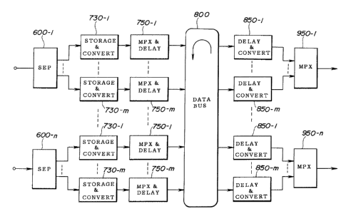
Figure 4 is a first embodiment of an optical switching
system according to the present invention. In Figure 4, wave-
length-division multiplexed signal separators 600-1 through 600-n
each enter an input optical signal which is a wavelength-division
multiplexed and time-division multiplexed signal and separate a
time-division multiplexed signal component in each of the divided
wavelengths. After separation of the time-division multiplexed
signal component, the wavelength-division multiplexed signal
separators 600-1 through 600-neach read a control information
,.~
- 7b - 27879-9
1313~9
included in the input optical signal and output an optical
signal corresponding to the time-division multiplexed signal
component.
optical storage and wavelength converters 730-1
through 730-m are coupled to each of the wavelength-division mul-
tiplexed signal separators 600-1 through 600-n and store optical
signals output from the wavelength-division multiplexed signal
separators 600-1 through 600-n for every time slot identical to
that used for the separation in the wavelength-division
multiplexed signal separators 600-1 through 600-n. The optical
storage and wavelength converters 730-1 through 730-m read out
the stored optical signals successively in a sequence of pre-
determined time slots and convert the wavelengths of the optical
signals to predetermined
- 8 - ~ g
1 wavelengths based on the control information.
Optical multiplexer and delay parts 750-1
through 750-m each multiplex the wavelengths of an
output optical signal of the corresponding one of the
optical storage and wavelength converters 730-1 through
730-m and output the optical signal after delaying the
phase of the optical signal a predetermined quantity.
An optical bus 800 enters output optical
signals of the optical multiplexer and delay parts 750-1
through 750-m and transfer these optical signals in a
predetermined direction in an optical transmission
path. In this embodiment, the optical transmission path
is a loop-shaped path.
Optical delay and wavelength converters 850-1
through 850-m are coupled to the optical bus 800 and
each extract an optical signal having wavelengths
belonging to a predetermined wavelength region and delay
the phase thereof a predetermined quantity so as to
convert the wavelengths of the optical signal into
predetermined wavelengths.
Optical wavelength multiplexers 950-1 through
950-n are each coupled to the optical delay and
wavelength converters 850-1 through 850-m and multiplex
the wavelengths of the optical signal so as to output an
optical output signal which is a wavelength-division
multiplexed and time-division multiplexed signal.
As a result, the output optical signal is
obtained with a space multiplexing factor n, a
wavelength multiplexing factor m and a time multiplexing
factor m. The optical output signal of the optical
switching system has a signal format approximately the
same as that of the original optical input signal. In
other words, the alignment of the optical wavelength,
the center wavelength, the wavelength bandwidth and the
like of the input optical signal and the output optical
signal of the optical switching system are approximately
the same.
- 9 - 1313~19
1 FIG.5 shows the first embodiment in more
detail. An optical input signal which is a wavelength-
division multiplexed and time-division multiplexed
signal is obtained from a plurality of channels. For
S the sake of convenience, FIG.5 shows a case where there
are two channels.
The optical input signal is made up of cells
having a fixed length and a header H as shown in FIG.6.
The header H contains information such as a wavelength
information ~1 f an optical input signal, a content
information A1, a wavelength information ~2 of an
optical output signal, an output channel information
a2, an information quantity ~1' a priority
information P, and a time slot information t2, ~nd
may be described as H(~l, Al, ~2~ a2' ~1~
f, t2, ...). The wavelength information ~2
includes ~21~ ~22' ~23' ... . The output
channel information a2 includes a21, a22, a23,
... , and may be used for making a broadcast. The time
slot information t2 includes t21, t22, t23, ... .
For example, the optical input signal received
from a first channel CHl is applied to an optical
wavelength-division multiplexed signal separator
(frequency divider) 60-1 wherein time-division
multiplexed data are separated from the optical input
signal in each of the divided wavelengths. Output
optical signals of the optical wavelength-division
multiplexed signal separator 60-1 are supplied to
detectors 65-1 through 65-3 which detect a control
information included in the optical signals. This
control information is used to control time slot
interchange and frequency shifters 70-1 through 70-3.
The optical wavelength-division multiplexed
signal separator 60-1 has a structure shown in FIG.7.
The optical wavelength-division multiplexed signal
separator 60-1 has an optical fiber 60-11, ring optical
resonators 60-121 through 60-12n respectively having
,
- 10 - 13133~9
1 ~center optical frequency fi (i=l, 2, ..., n and n=3 in
this embodiment), and optical fibers 60-131 through
60-13n. Each ring optical resonator 60-12i is optically
coupled to the optical fiber 60-11 and the corresponding
optical fiber 60-13i.
Each of the detectors 65-1 through 65-3 have a
structure shown in FIG.8A, 8B or 8C. In FIG.8A, the
detector 65-1 has optical couplers 65-11 and 65-12, an
optical local oscillator 65-13, an optical delay circuit
65-14, and a photodetector 65-15. The optical signal
from the optical wavelength-division multiplexed signal
separator 60-1 is output via the optical delay circuit
65-14. On the other hand, the control information is
extracted by the optical local oscillator 65-12 and is
output from the photodetector 65-15 in the form of an
electrical signal.
In FIG.8B, the detector 65-1 has an optical
coupler 65-21, an optical delay circuit 65-22, a
photodetector 65-23, a local oscillator 65-24, and
electrical tuners 65-251 through 65-25n. The optical
signal from the optical wavelength-division multiplexed
signal separator 60-1 is output via the optical coupler
65-21 and the optical delay circuit 65-14. On the other
hand, a portion of the optical signal (for example, 1/10
the optical power) is branched by the optical coupler
65-21 and supplied to the photodetector 65-23. The
electrical tuners 65-251 through 65-25n respectively
detect the modulation frequency of the header of the
optical signal responsive to an output of the local
oscillator 65-24 and output control information CI
through CIn.
In FIG.8C, ~he detector 65-1 has an optical
coupler 65-31, an optical amplifier 65-32, an FM/AM
converter 65-33, a photGodSetector 65-34, and electrical
filters 65-351 through ~4-35n having mutually different
passbands. The optical signal from the optical
wavelength-division multiplexed signal separator 60-1 is
~ 27879-9
output via the optical coupler 65-31. On the other hand, the
optical signal is branched by the optical coupler 65-31 and is
supplied to the FM/AM converter 65-33 via the optical amplifier
65-32. For example, a known semiconductor optical amplifier
may be used as the optical amplifier 65-32. For example, the
FM/AM converter 65-33 comprises a known element which passes an
optical signal having a predetermined wavelength. Thus it is
possible to convert a frequency modulated (FM) optical signal
into an amplitude modulated (AM) optical signal. The output
optical signal of the FM/AM converter 65-33 is converted into an
electrical signal in the photodetector 65-34, and the electrical
signal is supplied to the electrical filters 65-351 through
65-35n which respectively output control information CIl through
CIn .
Output optical signals of the detectors 65-1 through
65-3 are supplied to the corresponding time slot interchange
and frequency shifters 70-1 through 70-3. Each of the time slot
interchange and frequency shifters 70-1 through 70-3 have a
structure shown in Figure 9. The time slot interchange and
frequency shifter comprises a time-division multiplexed signal
separator 72, optical gate memories 73-1 through 73-100~ optical
frequency shifters 74-1 through 74-100, a wavelength multiplexer
75, and an optical delay circuit 76. In the embodiment shown in
Figure 9, the time-division multiplexed signal separator 72
separates 100 time-division multiplexed signals from the output
optical signal of one of the detectors 65-1 through 65-3.
, ~
- lla - 1 3 13 31 9 27879-9
The time-division multiplexed signal separator 72 functions
differently from the optical wavelength-division multiplexed
signal separator 60-1 or 60-2 in that the separator 72 merely
provides branching of the same signal. An output optical
signal or optical packet of the time-division multiplexed signal
separator 72 is successively supplied and stored in the optical
gate memories 73-1 through 73-100 in this sequence during
mutually different time slots. The optical data stored in the
optical gate memories 73-1 through 73-100 are read out based
on the control information described above and supplied to the
- 12 - 13133i9
1 corresponding optical frequency shifters 74-1 through
74-100 which convert the wavelengths of the input
optical signals into mutually different wavelengths.
Output optical signals of the optical
frequency shifters 74-1 through 74-100 are supplied to
the wavelength multiplexer 75 wherein a wavelength
multiplexing takes place. A wavelength-division
multiplexed optical signal output from the wavelength
multiplexer 75 is supplied to the optical delay circuit
76 which compensates for a phase error caused by
different input positions of the optical signals to the
optical bus 80. An output optical signal of the optical
delay circuit 76 is supplied to the optical bus 80 via a
corresponding one of optical couplers 77-1 through
77-3. ~ence, the optical signal from the optical delay
circuit 76 is transferred in a predetermined direction
in the optical bus 80.
The time-division multiplexed signal separator
72 has a structure shown in FIGS.10A and 10B. In
FIG.10A, the time-division multiplexed signal separator
72 has an optical amplifier 721 and a star branch part
722. The o~tical amplifier 721 includes a
Sa~l- ~rans ~a~e~
mirror 723 which receives a light for
optical pumping, an~ Er doped fiber 724, and an optical
filter 725. In FIG.10B, the time-division multiplexed
signal separator 72 has optical fibers 725 and
electrodes 726 provided on a chip 727. The output
optical signal of the time-division multiplexed signal
separator 72 is controlled responsive to a control
signal applied to the electrodes 726.
A known optical memory may be used for the
optical gate memories 73-1 through 73-lO0. For example,
it is possible to employ an all optical flip-flop
proposed by Odagawa et al., "All Optical Flip-Flop
Operation of Bistable Laser Diode", Extended Abstracts
of the 20th (1988 International) Conference on Solid
State Devices and Materials, The Japan Society of
- 13 - 13~33~9
l Applied Physics.
Each of the optical couplers 77-1 through 77-3
have a structure shown in FIG.ll. In FIG.11, the
optical coupler 77-1 has an optical fiber 77-10 which is
optically coupled to the optical data bus 80 at a
portion 77-11. One end of the optical fiber 77-10 is
connected to an absorbing part 77-12 which absorbs the
optical signal transferred within the optical fiber
77-10.
In addition, a known optical frequency shifter
may be used for the optical frequency shifters 74-l
through 74-100. For example, it is possible to employ a
wavelength conversion element proposed in Kuno et al.,
"Study on the Wavelength-Switching Devices Using
Bistable DFB Lasers", National Conference of
Semiconductor/Materials Group of Electronics and
Information Communication Society, 1987~or a wavelength
conversion element proposed in Kondo et al., "A Tunable
Optical-Wavelength Conversion Laser with TM-Polarized
Light Input", National Conference of Electronics and
Information Communication Society, Fall 1988.
Returning now to the description of FIG.5,
optically coupled bandpass filters 81-1 through 81-3
each output an optical signal which is obtained from the
optical bus 80 and has a wavelength in a vicinity of a
center wavelength thereof, that is, a wavelength within
a predetermined wavelength range. Optical signals
output from the optically coupled bandpass filters 8i-1
through 81-3 are supplied to corresponding optical delay
circuits 85-1 through 85-3 wherein a phase error
compensation similar to that described above takes
place. A known optical delay element may be used for
the optical delay circuits 85-1 through 85-3. Optical
signals output from the optical delay circuits 85-1
through 85-3 are supplied to corresponding optical
frequency shifters 90-1 through 90-3 wherein the
wavelengths of the optical signals are returned to the
- 14 - ~3133~
1 original wavelengths. Optical signals output from the
optical frequency shifters 90-1 through 90-3 are
supplied to a wavelength multiplexer 95-1 which
f~. ~ltiplexes the wavelengths of the optical signals~'
an output optical signal of the wavelength multiplexer
95-1 is transferred to an optical fiber (not shown), for
example.
Each of the optically coupled bandpass filters
81-1 through 81-3 have a structure shown in FIG.12. In
FIG.12, the optically coupled bandpass filter 81-1 has a
ring optical resonator 81-10 and an optical fiber
81-11. The ring optical resonator 81-10 is optically
coupled to the optical data bus 80 and the optical fiber
81-11. The optical fiber 81-11 transfers the passed
optical signal to the corresponding optical delay
circuit 81-1.
The wavelength multiplexer 95-1 has a
construction shown in FIG.13. The wavelength
multiplexer 95-1 has optical fibers 95-11 through 95-ln,
ring optical resonators 95-21 through 95-2n respectively
having~center optical frequency fi (i=l, 2, ..., n and
n=3 in this embodiment), and an optical fiber 95-3.
Each optical resonator 95-2i is optically coupled to the
corresponding optical fiber 95-li and the optical fiber
95-3.
The optical input signal received from a
second channel CH2 is processed similarly to the optical
input signal received from the first channel CHl. For
this reason, a description of an optical wavelength-
division multiplexed signal separator 60-2, detectors
66-1 through 66-3, time slot interchange and frequency
shifters 71-1 through 71-3, optical couplers 78-1
through 78-3, optically coupled bandpass filters 82-1
through 82-3, optical delay circuits 86-1 through 86-3,
optical frequency shifters 91-1 through 91-3, and a
wavelength multiplexer 95-2 will be omitted.
FIGS.14A and 14B respectively show the input
- 15 - 13i~19
1 optical signal and the output optical signal of the
first embodiment. In FIG.14A, signals Sl, S2 and S3 are
time-division multiplexed to a wavelength ~l of the
input optical signal, signals S1', S2' and S3' are
time-division multiplexed to a wavelength ~2 of the
input optical signal, and signals Sl", S2" and S3" are
time-division multiplexed to a wavelength ~3 of the
input optical signal. In FIG.14B, signals S2, S1' and
S3' are time-division multiplexed to the wavellength
~1 of the input optical signal, signals S1'~ S2" are
time-division multiplexed to the wavelength ~2 of the
input optical signal, and signals Sl", S2' and S3 are
time-division multiplexed to the waveiength ~3 of the
input optical signal.
When it is assumed that the optical input
signal received by the optical switching system shown in
FIG.5 has a multiplexing factor (a, b, c), where a
denotes a number of input optical fibers, b denotes a
number of optical frequencies which are multiplexed and
c denotes a time-division multiplexing factor, the
optical output signal of the optical switching system
has the same multiplexing factor (a, b, c). In other
words, in FIG.5, the optical input signal to the optical
switching system is divided into b optical frequencies
in each of the optical wavelength-division multiplexed
signal separators 60-1 through 60-a, where a=2 and b=3
in FIG.5. The b optical frequencies from the optical
wavelength-division multiplexed signal separator 60-i,
for example, are supplied to the corresponding b
detectors 65-1 through 65-b wherein a routing
information is extracted.
The routing information includes the number a
of output optical fibers of the optical switching
system, the number b of optical frequencies output from
the optical switching system and a time-division slot
address (time slot number) c at the time of output.
When the routing information is extracted in the
- 16 _ 13133~9 27879-9
detectors 65-1 through 65-b, the optical signal is stored in the
optical gate memories 73-1 through 73-c (c=100 in Figure 9) of
the control time slot interchange and frequency shifters 70-1
through 70-b for the time c which is in conformance with the time
slot number c. The stored optical signals are read out in the
sequence of the time slot number c.
The optical signals stored in the optical gate
memories 73-1 through 73-c may be read out at the same time, but
no problems are introduced thereby. This is because the optical
frequencies of the optical signal are all converted in the c
optical frequency shifters 74-1 through 74-c shown in Figure 9 so
as to carry out a routing in conformance with the extracted
routing information. The optical frequency shifters 74-1 through
74-c are optical frequency converters. The optical frequencies
are converted as shown in the following Table 1. In the Table
1, a subscript "111" means that the 111th optical frequency
(which is an optical frequency only used within the optical
switching system) is assigned to the optical signal. In this
case a=l, b=l and c=l. A subscript "112" is adjacent to the 111th
optical frequency and only the value of c differs by "1". In
other words, the number of optical fibers and the optical
frequencies at the time of output are the same as those at the
time of input, but the time slot number c increases by "1".
- 17 - 13~3~9
1 Table 1
Hlll H112 113 -- Hllc
121 H122 123 -- H12c
131 H132 133 -- H13c
5 .
Hlbl Hlb2 lb3 -- Hlbc
all Hal2 al3 Ha1c
a21 Ha22 a23 -- Ha2c
10a31 Ha32 a33 -- Ha3c
.~
abl Hab2 ab3 -- Habc
The routing information is included in a
portion of the header H shown in FIG.6. In other words,
the header H includes the routing information of the
above Table 1. The header H additionally includes an
information instructing a broadcasting of the same
information, a priority of the information, the size
(length) of the information and the like. For example,
when the header H includes the information instructing
the broadcasting of the same information, the optical
gate memory 73-1 for example is not only opened during
one time slot but is opened during a number of time
slots to send the information a plurality of times to
output a plurality of optical signals (a', b', c'), (a",
b", c"), (a, b, c), ... . In other words, the same
information is transferred for the number a' of optical
fibers, the number b' of optical frequencies and the
time slot number c. In the case of the information
having a high priority, it is~for example~possible to
give priority to the information over other information
by assigning a small number to a portion of the number
"abc".
Next, a description will be given of a second
embodiment of the optical switching system according to
the present invention, by referring to FIG.15. A
- 18 - 13~3319
1 description will first be given of the general principle
of this embodiment in conjunction with FIG.15~'and a
more detailed description on each of the elements
~ the optical switching system will be given
later in conjunction with FIG.16.
In FIG.15, detectors 100-1 through 100-n each
receive an optical input signal which is a wavelength-
division multiplexed signal and detect a control signal
included in the optical input signal.- The optical input
signals from the detectors 100-1 through 100-n are then
supplied to a corresponding one of first optical buses
150-1 through 150-m via optical couplers (not shown)z
The optical input signals are transferred in a
predetermined direction in a corresponding optical
transmission path. In this embodiment, the optical
transmission path is a loop-shaped path.
Optical bandpass filters 130-1 through 130-m
are respectively ins,erted in the corresponding first
optical buses 150-1 through 150-m and pass optical
signals in predetermined wavelength regions which are
determined by the eontrcl signals separated in the
detectors 100-1 through 100-n. Optically coupled
bandpass filters 300-1 through 300-n are coupled to each
of the first optical buses 150-1 through 150-m and pass
2S optical signals in predetermined wavelength regions.
Control signal detectors 330-1 through 330-n are coupled
to outputs of the corresponding optically coupled
bandpass filters 300-1 through 300-n and detect the
control signals included in the optical signals.
First wavelength shifters 360-1 ihrough 360-n
are also coupled to the outputs of the corresponding
optically coupled bandpass filters 300-1 through 300-n.
The first wavelength shifters 360-1 through 360-n each
delay the phase of the optical signal a predetermined
quantity and shift the wavelength of the optical signal
a predetermined quantity which is determined by the
control signal detected by the corresponding one of the
- lg - 13133~9 27879-9
control signal detectors 330-1 through 330-n. optical switches
390-1 through 390-n are coupled to outputs of the corresponding
first wavelength shifters 360-1 through 360-n and selectively
output optical signals to a second optical bus 410 via an optical
coupler (not shown) or to a corresponding wavelength shifter and
delay parts 220-1 through 220-n depending on the control signals
received from the control signal detectors 330-1 through 330-n.
The optical input signals received from the optical switches 390-
1 through 390-n are transferred in a predetermined direction in
a corresponding optical transmission path. In this embodiment,
the optical transmission path is a loop-shaped path.
Outputs of the wavelength shifter and delay parts
220-1 through 220-n are coupled to the corresponding first optical
buses 150-1 through 150-m via optical couplers (not shown). These
wavelength shifter and delay parts 220-1 through 220-n only
receive predetermined wavelength components determined by the
output control signals of the corresponding control signal detect-
ors 330-1 through 330-n. Each of the wavelength shifter and
delay parts 220-1 through 220-n shift the wavelength of the
received optical signal a predetermined quantity and delay the
shifted optical signal a predetermined quantity before outputting
the shifted optical signal to the corresponding one of the first
optical buses 150-1 through 150-n.
Second wavelength shifters 510-1 through 510-n are
coupled to the second optical bus 410. The second wavelength
shifters 510-1 through 510-n respectively receive from the second
- 19a - 13~19 27879-9
optical bus 410 optical signals having wavelengths within
predetermined wavelength regions. Each of the second wavelength
shifters shift the wavelength of the received optical signal a
predetermined quantity determined by the output control signal
of the corresponding one of the control signal detectors 330-1
through 330-n. Each optical wavelength multiplexer 550-1
through 550-p
- 20 - 1313319
1 are coupled to outputs of the second wavelength shifters
510-l through 510-n and subject~ the optical signal to a
wavelength-division multiplexing.
As a result, a wavelength-division multiplexed
optical signal (n waves) is obtained with a space
multiplexing factor p. The optical output signal of the
optical switching system has a signal format
approximately the same as that of the original optical
input signal. In other words, the wavelength bandwidth,
the center frequency, the time multiplexing factor and
the like of the input optical signal and the output
optical signal of the optical switching system are
approximately the same.
Next, a description will be given of the
second embodiment in more detail by referring to
FIG.16. For the sake of convenience, it will be assumed
that an optical input signal which is a wavelength-
division multiplexed and time-division multiplexed
signal having wavelengths l1 through ~ is
obtained from a channel CHl via an optical fiber (not
shown) and received by a detector 10-l. The detector
10-1 detects a control information A included in the
optical input signal. This control information A is
within the header H described before in conjunction with
FIG.6. The control information A is transferred to a
subscriber and used for various control including a
control of optical buses which will be described later.
The detector 10-1 may have the same construction as the
detector 65-1 described before.
An output optical signal of the detector 10-1
is supplied to an optical data bus 15-1 via a
directional optical coupler 11-1. The directional
optical coupler 11-1 may have the same construction as
the optical coupler 77-1 described before. The optical
signal is transferred in a predetermined direction
within the optical data bus 15-l which has a loop shape
in this embodiment. The optical signal which is
- 21 - 1 31 3 31 9
1 attenuated during the transfer within the optical data
bus 15-1 is amplified in an optical amplifier 12 which
is inserted in the optical data bus 15-1. For example,
a laser diode is used for the optical amplifier 12. In
a~dition, an optical bandpass filter 13 is inserted in
the optical data bus 15-1. The optical bandpass filter
13 is controlled by the control information A so as to
pass the optical wavelengths which transmit the desired
information.
The optical signal which has passed through
the optical bandpass filter 13 is supplied from the
optical data bus 15-1 to a directional optical coupler
31-1 via a directional optical bandpass filter 30-1
which has the functions of a directional optical coupler
and an optical bandpass filter (wavelength ~1 in this
case). The optical signal is branched in the
directional optical bandpass filter 30-1 and supplied to
an optical delay circuit 35-1 on one hand and supplied
to a directional optical coupler 32-1 on the other.
An output optical signal (for example,
wavelength ~ of 1.3~m) of an optical local oscillator
34-1 is supplied to another input of the directional
optical coupler 32-1 so as to carry out a heterodyne
detection with the output optical signal of the
directional optical coupler 31-1. An output optical
signal of the directional optical coupler 31-1 is
supplied to a photodetector 33-1 which outputs an
electrical signal corresponding to the control
information A.
The detectors 10-1 through 10-5 detect the
control information A by generally detecting the signal
information quantity, for example. The photodetector
33-1 also outputs the control information A but the
directional optical couplers 31-1 and 32-1 and the
photodetector 33-1 cooperate to read the header
information of the optical signal for each optical
frequency. Hence, the control information A obtained
- 22 - 27879-9
131;~3~9
from the photodetector 33-1 includes the routing information,
the information instructing the broadcasting of the same infor-
mation and the like.
On the other hand, the optical delay circuit 35-1
delays the optical signal a predetermined time tfor example,
10 1 ms) corresponding to a processing time of the processor. The
optical delay circuit 35-1 supplies a delayed optical signal to
an optical frequency shifter 36-1 so as to shift the wavelength
of the optical signal a predetermined shift quantity responsive
to the control information A. The optical frequency shifter 36-1
may have the same construction as the optical frequency shifter
74-1 described before. An output optical signal of the optical
frequency shifter 36-1 is amplified in an optical amplifier 37 and
supplied to an optical modulator 38-1. For example, a laser
diode is used for the optical amplifier 37. In order to improve
the accuracy of the optical signal, the optical signal is modulated
again in the optical modulator 38-1. An output optical signal of
the optical modulator 38-1 is supplied to an optical switch 39-1
which is switched responsive to the control information A.
The optical modulator 38-1 has a construction shown
in Figure 17. The optical modulator 38-1 has a substrate 38-10,
a pair of waveguides 38-11 and 38-12 formed on the substrate 38-10,
and a pair of electrodes 38-13 which sandwich the waveguide 38-
12. By applying a control voltage to the electrodes 38-13, the
optical signal passing through the waveguide 38-12 becomes delayed
with respect to the optical signal passing through the waveguide
- 22a - 13133i9 27879-9
38-11, and the optical signal supplied to the optical modulator
38-1 is subjected to an intensity modulation and output as a
modulated optical signal. It is possible to carry out a phase
modulation by simply omitting the waveguide 38-11.
The optical switch 39-1 has a construction shown
in Figure 18. The optical switch 39-1 has a
- 23 - 13~33~9
1 substrate 39-10, a pair of waveguides 39-11 and 39-12
formed on the substrate 39-10, and a pair of electrodes
39-13 provided at a branching portion of the waveguides
39-11 and 39-12. By applying a control voltage to the
electrodes 39-13, it is possible to selectively pass the
incoming optical signal to a selected one of the
waveguides 39-11 and 39-12.
When a priority P of the optical signal
supplied to the optical switch 39-1 is low and an
optical signal having a higher priority ~ exists in
another channel in FIG.16, the optical switch 39-1 is
switched to output the optical signal from the optical
modulator 38-1 to a feedback loop so as to supply the
optical signal to an optical bandpass filter 23-1. On
the other hand, when a priority ~ of the optical signal
supplied to the optical switch 39-1 is high and an
optical signal having a higher priority P does not
exist in another channel in FIG.16, the optical switch
39-1 is switched to output the optical signal from the
optical modulator 38-1 to an optical data bus 41 via a
directional optical coupler 40-1.
When the optical switch 39-1 is switched to
output the optical signal to the feedback loop, the
optical bandpass filter 23-1 passes the wavelengths
determined by the control information A. An output
optical signal of the optical bandpass filter 23-1 is
supplied to an optical frequency shifter 22-1 which
shifts the wavelength of the optical signal a
predetermined shift quantity determined by the control
information A. The optical frequency shifter 22-1 may
be constructed similarly to the optical frequency
shifter 36-1. An output optical signal of the optical
frequency shifter 22-1 is delayed a predeter~ined time
(for example, 10 2 ms) in an optical delay circuit
21-1 responsive to the control information A and is
supplied to the optical data bus 15-1 via a directional
optical coupler 20~1. The optical signal supplied to
-24- 27879-9
13133~g
the optical data bus 15-1 is transferred in the predetermined
direction and is supplied to the directional optical coupler
31-1 via the directional optical bandpass filter 30-1 when the
optical signal reaches the directional optical bandpass filter
30-1. The above described operation is repeated until the optical
switch 39-1 is switched to output the optical signal from the
optical modulator 38-1 to the optical data bus 41.
Next, the optical signal, which is obtained from the
optical switch 39-1 and is supplied to the optical data bus 41
via the directional optical coupler 40-1, is transferred in a
predetermined direction within the optical data bus 41. In this
embodiment, the optical data bus 41 has a loop shape. When the
optical signal transferred within the optical data bus 41 reaches
a directional optical bandpass filter 50 which passes the wave-
length ~1' for example, the optical signal is supplied to an
optical frequency shifter 51-1 via the directional optical band-
pass filter 50-1. The optical frequency shifter 51-1 shifts the
wavelength of the optical signal back into the original wave-
length. An output optical signal of the optical frequency shifter
51-1 is supplied to an optical multiplexer 55 together with output
optical signals of other optical frequency shifters 51-2 through
51-5. A wavelength-division multiplexed and time-division multi-
plexed optical signal is output from the optical multiplexer 55
and supplied to an optical amplifier Inot shown) via an optical
fiber, for example.
Operations similar to that described above are
-24a- 13 ~ 331 9 27879-9
carried out with respect to the wavelength-div.ision multiplexed
and time-division multiplexed signal which is received at the
other channels CH2 through CH5.
As a result, the input optical signal, which has
the time, space and wavelength thereof controlled and multiplexed,
is output from the optical switching system
- 25 - 1.313319
l with a format which is substantially the same at the
time when the input optical signal is supplied to the
optical switching system.
In the described embodiments, the optical data
5 bus has the loop shape. Hohwever, it is not essential
that the optical data bus has the loop shape.
According to the present invention, the rules
of frequency conversion are as follows. For the sake of
convenience, an optical packet routing information
10 within the header H is denoted by (a, b, c), and it is
assumed that an optical packet signal having a frequency
X is converted into an optical packet signal having a
frequency "abc". }Iere, a denotes a number of output
optical fibers (number of output highways), h denotes an
15 output optical frequency (output highway freqency), and
c denotes an output time slot (output highway time
slot). The optical frequencies of all the optical
packet signals are converted depending on the optical
packet routing information (a, b, c), and the converted
20 optical frequencies are sequentially arranged depending
on the values of "abc" as shown in the following Table
2. ~ Table 2 shows the optical packet arrangement in
the optical data bus.
Table 2
25 (a,b,c) = ~ Time c
a=l~a (lll), (112), (113), .. , (llc)
, (121), (122), (123), .. , (12c)
Freq. b (131), (132), (133), .. , (13c)
~bl), (lb2), (lb3), ... , (lbc)
Fiber a-Group
. . ~
(all), (al2), (al3), ..., (alc)
(a21), (a22), (a23), ..., (a2c)
Freq. b-Group~ (a31), (a32), (a33), ..., (a3c)
(abl), (ab2), (ab3), ..., (abc)
- 26 -
~3i~3i9
1 the same output highway signals (packets) have the same
first digit as "a##" in the optical data bus (800 and
80, for example). The group is named the a-group as
shown in the Table 2. In the a-group, the packets of
S the same output highway frequency have the same first
two digits as "ab#" and this group is named the b-group.
Further, the present invention is not limited
to these embodiments, but various variations and
modifications may be made without departing from the
scope of the present invention.