Note: Descriptions are shown in the official language in which they were submitted.
1313430
A P}~OTONIC SWll'CH ARCHlTECTURE
UTILIZING CQDE AND WAlVELENGTH MULTIPLEX~IG
Technical Fieldl
This invention relates tO arrangements for multiplexing and
S demultiplexing electrical and optical signals.
Problem
Optical systems are increasingly being used for transmitdng large
quantities o~ information represen~ing voice, video, and data The demands for
bandwidth on such optical systems keep growing as these systems are used, for
10 example, for transmitting a large number of channels for cable television systems.
In the future, such systems may be further burdened as high definition television
signals become more prevalent and as the number of chaDnels to be provided
continues to grow. Such arrangements put an increasing burden on the amount of
inforrnation which must be transmitted over the optical fiber.
Optical transmission systems, in contrast to coaxial cable systems,
almost invariably use digital signaling to transmit information. Among the
multiplexing schemes which can be used to multiplex a large number of digital
signals onto a single lightwave camer system is code division multiplexing. Codedivision multiplexing is a process whereby a number of input signals are each
20 orthogonalized before being added together, so that each signal can later be extracted
individually, uncorrupted by the presence of the other signals. Extracdon is usually
accomplished thIough a correlation process. l'he coding is usually accomplished
through a special code sequence which multiplies the input signal or phase
modulates the carrier of the input signal.
Another arrangement for multiplexing a number of different signals onto
an optic transmission system is to use wavelength division multiplexing whereby
each group of digital signals modulates a different wavelength of light and all the
waveleng~s are carried simultaneously on the optic fiber.
However, even with the best available opdc ~ansmission moduladon
30 systems, there still is a need for additional bandwidth and further there is not a
satisfactory economical arrangement for extracting a specific signal from an optic
~ansmission system which is carrying a large number of different signals. The latter
function is required, for example, for a receiver of cable television signals.
-` 1313~30
Solution
The above problems are solved and an advance is made in the state of
the art in accordance with principles of my invention wherein, illustratively, acombination of code division and wavelength (frequency) division signals is carried
5 by an optic transm~ssion or switching system and wherein, advantageously, a merged
decoder is used for extracting the signal carried by any code of any wavelength of
the optic system. The decoder comprises a group of optical modulators each tunedto a different wavelength; only one of these optical modulators corresponding to the
desired wavelength is made active. The output of that optical modulator is combined
lû in a phase shifter with the code sequence of the selected signal. Wh~n the output of
the phase shifter is combined with the input signal in a P~ photodiode ~or opticdetection, the electrical output of the PIN diode represents the desired signal.More generally, these aIrangements of encoders and decoders can also
be used for electrical systems. Since w avelength and frequency are related, it is
15 possible to refer to either. For convenience, and because the exemplary embodiment
uses photonics, wavelength is used through this specificadon.
In accordunce with one aspect of the invention combined code and
wavelength division modulation is achieved by a combination of a plurality of code
division multiplexers acting as inputs to a wave division multiplexer. Each code20 division multiplexer comprises a plurality of phase shifters, each of which have a
signal înput and a code sequence input. The output of these phase shifters is then
combined in a passive optical coupler which is used as one of a plurality of inputs tO
a wave division multiplexer. The wave division multiplexer comprises a series ofwavelength converters for taking the outputs of the code division multiplexers, all of
2S which are at the same wavelength, and converting these outputs to the di~ferent
wavelengths. The ou~puts of the wavelength converters are then c~mbined with a
passive optical coupler.
In accordance with another embodiment of the invention, a switch
comprises a combined code division and wavelength division multiplexe~ whose
30 output is connec~ed to the input of a plurality of the code division/wavelength
division decoders.
In accordance with another aspect of the invention, a switch for
extracting and inserting a plurality of signals into an optical transmission system is
implemented as follows. The outputs are extracted USillg a plurality of the merged
3S decoders as described above. Inputs are added by generating standard outputs of the
code division multiplexers and converting their wavelength to ones of the
13~3430
..
wavelengths not used in the output of the switch. These outputs are then combined with
inputs used in the output of the switch by a passive coupler. Advantageously, such an
arrangement permits a large number of signals to be added and extracted at one point in
an optical transmission system.
In accordance with another aspect of the invention, signals are maintained
in the optical domain throughout the encoding process and through the decoding process
- until the output of the demodulator which is an electrical output is produced by the
decoder.
In accordance with one specific embodiment, the phase shifter is a lithium
niobate device having electrical inputs representing the code sequences applied at the
electrodes of a phase shifter in which a basic lithium niobate crystal has a titanium
di~fused waveguide that passes through the crystal. The titanium at the surface is
surrounded on the two sides by the electrocles containing the electrical signal that
represents the code sequence. In accordance with one aspect oE the invention, the
merged decoders can be wklely clistributecl to a number oE stations which receivc, a
broadcast wiclebancl signal. Such an arrangement provides the capability for any station to
extract the desired signal from the large number of signals being transmitted.
In an alternative embodiment oE the combined decoder, optical OUtp~lt is
produced by using in series a tunable optical filter for selecting the wavelengEh, a
wavelength converter for converting the selected wavelength to a standard wavelength,
and a phase shifter, responsive to a selected orthogonal input sequence for selecting the
desired signal.
Therefore, in accordance with the principles of this invention, a
demultiplexer of a combined wavelength (frequency)/code division multiplex signal
comprises a wavelength selector, for selecting the correct wavelength, which clrives a
combining circuit for combirling a selected orthogonal sequence with the selected
wavelength signal, and the output of the combiner is used to extract the desired output
signal from the multiplex signal. A multiplexer comprises a plurality of code division
multiplexers, each driving a wavelength converter for generating a signal at a different
wavelength, and a means for combining the outputs of the wavelength converters to
generate the multiplexed output signal.
1313430
3 a
In accordance with one aspect of the invention there is provided a two-
stage multiplexer for multiplexing a plurality of input s;gnals to generate an output signal
comprising: a plurality of first means, each means responsive to a plurality of said input
signals for generating an intermediate signal comprising a plurality of code division
S multiplexed signals; and second means for combining the intermediate signals to generate
the output signal, comprising a plurality of wavelengths, each ~;vavelength for carrying the
intermediate signal of one of the first means; wherein the input signals comprise
modulated optical input signals, and wherein each of the first means comprises: a plurality
of means for phase shifting an optical signal, each means responsive to a modulatt,d
10 optical input signal and to one of a plurality of orthogonal code sequences for generating
a modulated lightwave output signal, and third means comprising optical amplification
means for combining the modulated lightwave output signals oE the plurality of phase
shiEters for generating the intermetliate signal.
Brief ~escril~tion of the l)rawin~
:~5 FIG. 1 is a conceptual ~liagram of a code division switch;
.:; r~
I
,, 1313430
~;IG. 2 is a dia~am of a photonic code division switch;
FIG. 3 is a diagram of a photonic code division multiple~er,
FIG. 4 is a diagram of a photonic code division/wavelength division
switch;
S FIG. 5 is an illustration of a phase shifter for use in a code division
multiplexer and demultiplexer;
FIG. 6 is a diagram of a wavelength multiplexer;
FIGS. 7 and 8 are diagrams of code division/wavelength division
demultiplexers; and
FIG. ~ is a diagrarn of an addldrop multiplexer.
Detailed Description
1. Introduction
. _ _
The use of Code Division Multiplexing (CDM,~ in a photonic switch has
been described in T. K. Gustafson and P. W. Smith, Photon~c Switchin~ (book),
Springer-Verlag, 1988, pp. 167-70. CDM can be used to make each input channel
orthogonal to every other input channel so that the surn of all the orthogonalized
input channels can be presented to a decoder at each output port of the switch. The
actual output signal on each por~ can be selected to be any one of dle input signals by
using the appropriate code for selection. This is possible because of the co~relalion
20 property of an orthogonal code family.
T
f ~i~j(t)dt = 1 for i = j
= O for i ~ j
~i and ~j are members of the code family that are used to orthogonalize the input
bits, and T is the duration of any code sequence and the duration of any input bit.
25 This is the means by ~vhich any input signal can be switched to any or all out3~uts
(customers). ~erefore, the resultant switch is non-b~ocking with broadcast
capability.
The basic s~ucture of a switch that uses an orthogonal code family is
shown in FIG. 1. Members of a first g~oup of n multipliers 100 are each connected
30 to one of the inputs, input 1, input ~,...input n, and to a memb~r of the ordlogonal
code sequence set, ~1 (t),~2(t),...,~n(t), respectively. The outputs of each of the n
multipliers are connected to a summing circuit 102 whose output in ~urn is connected
to a second group of multipliers 100, each of which has as one input the sum signal
1313430
(i.e., the output of summing circuit 102) and an appropriate one of the code
sequences for selecting the desir~d signal. 'Ihe output of e~ch second block 1~ is
connected to an integrator 107 whose output represents the selected signal, i.e., the
input associated with the coding sequence that is applied to ~e multiplier 100.
S In mathematical terms, the input signals are each multiplied by the
different members of the orthogonal code family. Therefore, the orthogonalized
inputs can be represented as ~j(t~ x input bits, where the input bits are a 1 or -1 for a
duration of T, and ~i(t) = 1 or -1 for a duration l'ln. If the input is a baseband
signal, the output is a baseband signal of n times the input bandwidth.
Therefore, an input to the summing circuit can be expressed as,
mj(t)~j(t) (2)
where mi(t) is the informaeion (~1 or -1) and ~j(t) is the orthogonal code for input
channel i. The output from a multiplier on the right of FIG. 1 that is also fed with
~i(t) is:
ml (t)~l (t)~i(t) + .' ~ mi-l (t)q)i-l (t)~i(t)
+ mi ~t)~i2 (t) + mi+l (t)~hl (t)~i (t) + -
All the unwanted cross terms with ~i (t)~j (t) will integrate to zero from equation 1,
and the output from the integrator in FIG. 1 becomes:
~li(t)q)i2(t). (4)
20 If ~i(t) is a polar orthogonal code sequence, ~i2(t) is unity. Therefore, the decoder
output becomes mi(t).
If the input entering one of the ~st blocks 100 of FIG. 1 is in optical
form, it is already modulated typically as on-off keying or phase shift keying (PSK).
Since the ~1 (t) waveforms repeat for each information bit, the output from any of the
25 multipliers on the left is a PSK signal modulated at the rate determined by ~i(t).
This happens because ~ ) will either multiply the input by a +l or -1. A PSK signal
can be represented by using an optical carrier cos~ct in equation 2; equation 2
becomes ~i(t)mi(t)cos~ct = ~coso~ct and equa~ion 4 becomes:
mi(t)~i2(t)Cos2oct = 2~ ) (1 + cos203ct~,
,., ~ ' ~
- " 1 31 3~30
sincç the coherent detection of the optical signal is being performed by injecting
both the optical information signal and the optical carrier into a Posidvely doped-
Intrinsic-Negadvely doped (PIN) photodiode which approximates a multiplier if the
optical carrier is much larger than the optical information signal. Aft~r the output
S integrator, m; (t)/2= +1/2. This is an electrical domain version of the desired polar
input signal multiplied by one half. There are times when it is desLrable to stay in
the optical domain. The following technique can be used !to accomplish this goal.
If the input is in optical form, i~ is already modulated typically as on-off
keying (intensity moduladon) although phase shift keying (PSK) is pr~ferred for
10 coherent optical communications. In either case, a bandpass system rather than the
baseband system of FIG. 1 is required. Since the ~i~t) wavefomls repeat for each bit,
the output from any of the multipliers on the left of the new b~ndpass version of
FI5. 1 is a PSK signal modulated at the rate determined by ~i(t). This happens
because ~i(t) will either multiply the input by a ~1 or -1. For a PSK signal equation
15 2 becomes ~i(t)mi(t)cosc~ct = icosc~ct and equation 4 becomes,
mi(t)~i2(t)cos~ct = mi(t)coscoct
after the output bandpass integrator. 'l'his is a modulated version of the desired polaF
input. In actual optdcal implementadon, a phase shifter can be used to make the high
frequency PSK op~cal signal under the control of the high frequency orthogonal
20 code that repeats within a given information bit interval. Further, the decoder can be
another phase shifter followed by a narrow band opdcal filter if it is desired to
maintain a continuous optical path between input and output.
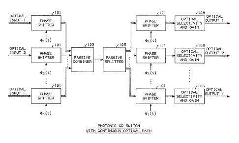
This is illustrated in FIG. 2 which shows physical instead ~f
mathematical elements. The phase shifters 101, the equivalent of the multipliers 100
25 of FIG. 1 are each con~rolled by a separate orthogonal sequence ~1 (t),~2~t),...,~n(t).
The ou~put of phase shifters 101 are connected to a passive combiner 103,
comparable to the surnmer 102 of FIG. 1. The output of passive cornbiner 103 is
connected to the input of passive splitter lOS whose outputs are the inputs to the
second group of phase shifters 101. l~e outputs of each member of the second
30 group of phase shifters 101 is connected to a circuit 108 for providing opdcal
selectivity and gain.
If it is required to add more inputs to this type of a code switch, it is
necessary to increase the bandwidth requirements of the switch proporiionally.
Therefore, the switch size on the input becomes limited by the bandwidth of the
~-`` 1 31 3430
individual components that are available to implement the switch. The oueput size of
the switch is limited by the losses associated with the combining circuit 103, and
power splitting in the passive splitter 105.
One strategy for a switch design or tlansmission system design that
5 must accommodate a large number of input channels is to group the input channels
into m groups of n channels. The total number of input channels that this switchcould handle is equal to n x m. A CD multiplexer is udlized for each group of n
channels, and n is chosen to produce a high frequency operation consistent with the
bandwidth of the technology that is used for implementadon. This approach makes
10 the speed requirement, and therefore the bandwidth, of the circuitry needed to
implement a switch with n x m inputs equal to the r~uirement for an n input CD
multiplexer; a speed reduction by a factor of m compared to that of a CD multiplexer
that must handle n x m inputs. A CD multiplexer 109, is shown in FIG. 3, and
comprises a plurality of phase shifters 101 and a passive combiner 103.
FIG. 4 shows a complete n x m switch comprising m CD
multiplexers 109, each with n inputs as shown in FIG. 3; a wavelength d;vision
(WD) multiplexer 201, discussed hereinafter with respect to FIG. 6; and a passive
spl;tter 105 for distributing the output of WD multiplexer 201 to lc different
combined wa~elength/code division demultiplexers 205, discussed hereinafter with20 respect to FIG. 7. The number of output ports, k, is limited by the fanout capability
from the wavelength division multiplexer 201 and passive splitter 105. If the passive
splitter cannot provide sufficient power to each output port, optical amplificadon is
used to boost the power.
Wavelength division multiplexing (WDM) is the name given to
25 ~equency division multiplexing in the optical dornain and can also be used in the
electrical domain since frequency and wavelength are related. There is great interest
in WDM by the use of coherent lightwave communication. The main reason is that apotentially large number of channels can be multiplexed and subsequently
demultiplexed (separated) because the high selectivity filtering requirements can be
30 accomplished in the elec~ical domain after the photodetector. This avoids thenecessity for high selectivity in ehe optical domain. However, if a switch or
transmission system with a large number of inputs is ne~ed, there is a requirement
for a large number of stable light sources to make each input orthogonal to every
other input by translating each input channel to a different wavelength~ The switch
35 or transmission system outputs are selected by coherent detection of the optical
signal. ~is requires a coherent carrier that is the proper frequency (wavelength) and
;
1 31 3430
- 8 -
phase. This in turn requires a large number of tunable lasers that can be phase
locked pr~erly or the multiplexing of a stable replica of each fre~quency
(wavelength) on each output port for demodulation.
An advantage can be obtained by utilizing both CDM and WDM
5 techniques because both can share a common detector (PIN) and the number of
precision lasers needed for modulation and detec~on can be reduced by a factor of n
by combining the two techniques in a single switch, as illustrated in FIG. 4.
The output fiber from the WD multiplexer cames m wavelengths and
each wavelength is modulated with n CDM input channels. There~ore, every output
10 is presented with all n x m inputs to the switch, and the switch has broadcast
capability. Purther, the speed requirements of CDM and the numbe~ of precision
lasers required for WDM are both moderated by combining or merging CDM and
WDM. Before consideling the merged CD/WD architecture further, it is noted that
the basic architecture illustrated in FIG. 4 can also be used to make a code
15 div;sion/space division (CD/SD) switch by replacing the WD multiplexer with anon-blocking space switch. Now the demultiplexer on the right of FrG. 4 is just for
CD and the output could stay in optical form if desired.
2. Code DivisionlVVa~elen~th Div}sion Architecture
The basic merged code/wavelength division architecture is illustrated in
20 FIG. 4. The code division multiplexer 109, illushated in detail in FIG. 3, can be
implemented by using one member of an orthogonal code family to modulate each
information bit by shifting the phase of the optical camer during the Wt interval to
be in phase half of the time and 180 degrees out of phase during half of the bitin~erval time. This phase shift is controlled by one unique sequence from an
25 orthogonal code farnily for each input channel. The rcsultant signal will be inphase
during the time when the code has logical zeros and out of phase when the code is
producing logical ones; this is phase shift key (PSK) modulation. This results
because of the polar nature of the q, signals; then two states are +1. When the
incoming carrier is muldplied by +l, its phase is unaffected; when multiplied by -1,
30 a 180 phase shi~t is effected. Thus the phase shift circuit 101 of FIG. 3 is equivalent
~o the multiplier 100 shown in FIG. 1. Next, all the input signals that have been PSK
modulated in bl~k 101 a~e added together in a passive combiner 103 comparable tothe summer 102 of FIG. 1, to form the CD multiplexer 109.
The phase shifter can be realized by utillzing titanium diffused
35 waveguides in lithium niobate with metal electrodes on ~he surface near a portion of
the titanium chaDnel. There is a change in the index of refraction of the material
1 31 3~30
g
when an electrical signal is applied to the electrode, this produces the desired phase
shift in the optical signal tha~ is propagating in the waveguide.
The device is illustrated in FIG. S which shows a lithium niobate phase
shffler for phase shift keying the optical signals. A lithium niobate crystal 503 has a
5 narrow and shallow titanium indiffused waveguide 505 along its length. The
waveguide is surrounded on two sides by electrodes 507 and 508 which are
connected to the electrical modulating signal. The optical input signal is injected at
one end of the waveguide and the ouq~ut appears at the othPr end.
The output ~>f the phas~ shifter is the desired phase shift keyed (PSK)
10 optical signal. Each orthogonal code word that controls the phase of the incoming
signal lasts for exactly the duration of an information bit, and then repeats for the
nex~ and all subsequent inforrnation bit time intervals. The bandwidth of each coded
input channel is increased by a factor that equals the number of bits in the length of
the orthogonal code family. However, all the coded input channels occupy the sarne
15 spectral density (frequency range). Further, all the coded channels may be added
together and later be separated by correlating each coded channel with the
appropriate rnember of the code family that was used for encoding, as suggested by
equation 4. This will be performed on the output of the switch to select any input
that is desired. However, the center bloek in PIG. 4, the wavelength
20 multiplexer 201, will be described firs~.
The function of the wavelength multiplexer 201, shown in detail in
FIG. 6, is to shift the wavelength of the incoming channels from ~e value ~0, that is
used for transrnission, probably 1.3 or 1.5 llm, to one of the selected values,
~1, ..., ~m- for wavelength multiplexing, using a plurality of wavelength
25 converters 501, addidvely combined by a passive combiner 103. The ou.tput of the
WD multiplexer is a single optical signal that contains the sum of the outputs from
the ~D multiplexers; each CD multiplexer output is translated to a predeterminedwavelengdl by the multiplexer.
The output signal from the WD multiplexer 2û1 in FIG. 4 is passed
30 through a passive splitter lOS that splits the signal into equally weighted parts, one
for each demultiplexer 205. Each demultiplexer 205 has as inputs representing the
wavelengt}ls ~ , and a selected code sequence, one of the k code sequences
)(t),~j(2)(t),...,~ ,)(t). Each demultiplexer 205 drives an attached laser and
electronic circuit 207 tO genera~e an optical output. The output circuitry combines
35 the demultiplexing of both the code division and the wavelength division processes
in one detector.
1 31 3430
.
The circuit of block 205 is shown in FIG. 7. The circuit includes m
optical modulators 701 each with an input of one of the wavelengths ~l, ..., ~m and
each having an attached control signal so tbat only the selected one of these optical
modulators is turned on. These optical modulators are lithium niobate optical
S modulators in the exemplary embodiment of the invention. The output of these
optical modulators is combined in a passive coupler 103 which is connected to a
phase shifter 101 whose other input is the selected code sequence. The output of this
phase shif~er is then connected to the PIN detector 707 which combines this signal
with the combined optical input signal to generate dle selected elecerical oulput.
10 This electrical signal now feeds block 207 (FIG. 4) which contains the appropriate
and well-known elec~onics to filter, amplify, and drive a laser di~e also contained
in block 207.
A passive splitter 105 may not provide sufflcient energy to drive the
required number of demultiplexers. In that case, an optical amplifier would be
15 required at the input to passive splitter 105. A traveling wave or Fabry-Perot optical
amplifier can provide the required amplification. This is described in G. Eisenstein
et al.: "Measurements of the Gain Spectrum of Near-Traveling Wave and Fabry-
Perot Semiconductor Optical Amplifiers at 1.5 ~m, " International Journal of
Electronics, vol. 60, no. 1 ,1986, pp. 1 13- 121 .
A PIN or avalanche photo diode (APD) fO7 (PIG. 7) is used to perfonn
the coherent detection needed for demultiplexing both multiplexing schemes (bothCD and WD) simultaneously. This is accomplished by selecting a p~rtion of the
same source that is used in ~he waveleng~ multiplexing process illustrated in FIG. S
as a second signal to be fed into the PIN. Since the diode produces an output
25 electrical signal that is proportional to the input optical power input, it is acting as a
square law device. The detector output, E(t), is given by the following expression.
~2
E(t) = l[A + m(t)]cOs~ctJ
[A2 + 2Am(t) + m(t)2~
( 1 + ~os2cl)0 t)
30 A is the optical calTier amplitude and m(t) is the information signal. The lowpass
filter output yu(t) is
~313430
y (t) = A2 ¦1 ~ 2m(t) ~ m(t)2 ]
It is obvious that there is a distortion term present in the conventional fo~n of optical
homodyne detection that is not present in the pure produc~ detector that is nonnally
used for elec~ical homodyne detection. However9 if the optical carrier is made large
S enough, m(t)/A~l, compared to the optical infonnation signal, this distortion ~erm
can be made negligiMe. Therefore, the optical canier needs to be sufficiently larger
than the infQrmation signal to ensure reliable digital detection. Also, if the LPF is
AC coupled, the output is given by the following.
yo-Am(t) ~,
10 FIG. 6 is a block diagrarn of wavelength division multiplexer 201 of
FIG. 4. Each of a plura}ity of s;gnals at wavelength ~0 is connected to a wavelength
converter 501 to generate a signal at one of the wavelengths ~ m, which ate
cornbined in combiner 103. Wavelength division multiplexers are known in the
prior art and described, for example, in I. Bar-Joseph et al:
15 "Self-electro-optic Effect Device and Modulation Converter in InGaAs/LrlP Multiple
Quantum Wells", Applied Physics Letter, vol 52, no. 1, 4 January 1988, page 53.
These wave division multiplexers comprise rneans for changing the wavelength of a
modulated signal such as an integrated circuit with two multiple quantum well
(MQW) diodes 601 connected in series, one of the diodes comprising matçrial
20 responsiw to an input wavelength, the other diode comprising material responsive to
the desired output wavelength.
FIG. 8 shows an alternative embodiment of a CD/WD
demultiplexer 800, operating in the opdcal domain. If demultiplexer B00 is used
instead of demultiplexer 205 and laser and elect~onics 207, then ehe switch of PIG. 4
25 operates in a fashion to provide a continuous optical path from input to ou~ut.
Demuldplexer 800 comprises a ~nable optical filter 801, operative under electrical
control, for selecdng a wavelength. This wavelength is transmitted to ~ wavelength
converter 501 whose output is a light signal of the standard wavelength ~. If the
wavelength converter 501 cannot be made sensitive to all outputs of the tunable
30 filter 801, then a group of wavelength converters 5û1 can be placed in parallel and
the appropriate converser output gated for transmission to phase shifter 101. The
output of wavelength converter 501 is tnen transmitted to phase shifter 101,
~ 3 1 3430
controlled by an electrical signal representing the selected orthogonal sequence ~i.
The OUtpllt of phase shifter 1()1 then is a light wave of the standard wavelength ~0,
modulated only by the selected signal. Tunable optical filters are well known in the
art and are discussed, for example, in S. R. Mallinson: "Wavelength-Selective Filters
5 for Single-Mode Fiber WDM Systems Using Fabry-Perot Interferometers", Applied
Optics, vol. 26, no. 3, February 1987, pages 430-436; F. Heismann et al.: "Narrow
Band Double-Pass Wavelength Filter With Broad Tuning Range", Integrated and
Guided Wave Optics Conference Record, Santa Fe, New Mexico9 March 28-30,
1988, pages 103-106; and W. V. Sorin et al.: "THB4 Tunable and Single-Mode Fiber10 Reflective C;ating Filter", Inte~rated Optics and Optical ~iber Communications
Conference, Reno, Nevada, January 19-22, 1987, page 194. Alternatively, the
relative positions of the wavelength converter and phase shifter may be reversed; the
arrangement shown in FIG. 8 offers the advantage of permitting a phase shifter to
work at one wavelength.
The switch architecture des-~ribed above merges CDM with WDM to
moderate the more difficult requirements of each approach when a large switch ortransmission system is re~quired. A potential application for an optical switch in the
local environment is likely in the 1990's since broadband ISDN (B-ISDN) is likely
to become a reality in the early or rnid 1990's. Such a system requires individual
20 video channels with a n~inimum data rate o~ 45 Mb/s for present TV signals and data
rates as large as 400 Mb/s are expected for high definition TV (HDTV) signals. It is
likely that a rate of about 140 Mb/s will be used as a common rate for both the USA
and Europe. These systems will use switches that may require approximately lO0
inputs to be compedtive with CATV systems. Further, it is likely that an enhanced
25 level of TV quality (preferably high definition quality if the cost is not too high) will
be required to show product improvement for E~-ISDN over the present CATV.
These inputs should be switched to hlmdreds and perhaps thousands of
outputs (customers). If 16 channels are CD muldplexed together on the input of aswitch illustrated in FIG. 4, and six wavelengths are used in the WD multiplexer, the
30 switch can accept 96 input channels. These inputs can be sent to any of hundreds
and potentially thousands of outputs if the fanout capability of the technology used
will pelm~t.
Instead of making one code switch that will accept 96 inputs and require
processing at 96 times the data rate of the input channels (as high as 96 x 140 Mb/s -
35 13.4 Gb/s,~, the resultant upper lirnit for data rate is only 16 x 140 = 2.24 Gb/s.Alternatively, if a WD switch were used for all 96 inputs, it would require
1 3 1 3~30
- 13-
96 wavelengths, multiplexed lasers OT tunable phase-locked lasers. However, thisswitch only requires 6 wavelengths.
The output ports of the merged switch are almost the same complexity
as if a CD or WD switch were implemented and the input ~ports only requirç simple
5 phase shifters, a rela~vely simple device. Since the center stage only requires
6 wavelengths in a WD multiplexer, it is simpler than a pure WD switch. The result
is a switch that could be implemented if the fanout requirements can be met. Thefanout requirements equal the number of switch outputs (customers).
The aIrangement of FIG. 4 can be used as a switch with a plurality of
lû inputs to each of the CD multiplexers 109 and a plurality of outputs, one from each
of the combined demultiplexers 205. For applications such as cable television, the
output of the WD demultiplexer 201 is connected to a fiber for distribution and each
of the demultiplexers 205 are connected to a tap on that cable.
For add-drop multiplexing applications in which a plurality of signals
15 are withdrawn at a switch and another plurality of signals are injected into the optical
signal at that switch, the configuration of FIG. 9 may be used. In this example, an
incoming light signal has components at wavelengths ~ 3, ~4 and ~5.
Additional optical inputs 1 l,...,ln and 21,...,2n are multiplexed in CD
multiplexers 109 of FI&. 1. The outputs of the two CD multiplexers 109 of FIG. 920 are each connected to one of two wavelength converters 501 which have outputs at
wavelengths ~4 and ~5 respectively. Three filters 901 are used to preserve the
2 and ~3 components of the incoming light signal. The outputs of these
filters 901 and the two CD multiplexers 109, are then com~ined in passive
coupler 103 to produce a lightwave output at wavelengths ~ 2. ~3, ~4 and ~5 .
25 To extract signals from the incoming lightwave, the incoming lightwave is
connected to passive splitter 105 which is connected to a plurality of CD/WD
demultiplexers 205 to generate output signals l,...,p. This is similar to the method of
extracting signals described with respect to FIG. 4. This arrangement then permits
another source to generate signals conveyed at the ~ 2, and ~3 wavelengths, and
30 the source of FIG. 9 to generate signals conveyed at the ~4 and ~5 wavelengths. The
optical circui~y of the multiplexer arrangement of FIG. 9 ex~acts input signals
calTied at the ~ 2 and ~3 wavelengths and injects new optical signals at ~4 and ~5
wavelengths. The light may be carried, for example, over a photonic ring
interconnecting the various signal sources and destinations.
1 31 3430
- 14-
It is to be understood that the above description is only of one p~efeIred
embodiment of the invention. Numerous other a~rangements may be devised by one
skilled in the art without departing from the spint and scope of ~e inven~on. The
invention is thus lirnited only as defined in the accompanying claims.
; ~;