Note: Descriptions are shown in the official language in which they were submitted.
1 3 1 3563
., 1
The present invention relates to a liquid crystal
display panel which is used as a display panel in a
liquid crystal TV and the like, more particularly, to a
thin film transistor panel which uses thin film tran-
sistors as switching devices for causing pixels in thepanel turn-ON and turn-OFF.
A thin film transistor panel which is used in
active matrix type liquid crystal display device for
displaying television image and the like is formed by
aligning a large number of transparent pixel electrodes
and a large number of thin film transistors for driving
the pixel electrodes in row and column directions on a
transparent substrate. Gate and drain electrodes of the
thin film transistors are connected to gates and data
lines which are wired between columns of the pixel
electrodes, and source electrodes are connected to the
transparent pixel electrodes.
A panel which is formed by aligning thin film tran-
sistors and pixel electrodes in row is widely known as
the thin film transistor panel. However, it was pro-
posed recently that the panel is constructed by forming
thin transistors on the transparent substrate, then form-
ing transparent insulating film thereon and then forming
transparent pixel electrodes on the transparent insu-
lating film. When the transparent insulating film isformed between the thin film transistors and the pixel
electrodes, aperture ratio of liquid crystal display
1313563
-- 2
device can be improved due to large area of pixel
electrodes since the short-circuit between the pixel
electrodes and the gates and data lines can be prevented
by the transparent insulating film even if the distance
therebetween is reduced.
The thin film transistor panel can be manufactured
by the following steps of: forming thin film transistors
on a transparent substrate, forming a transparent insu-
lating film thereon, providing contact holes through the
transparent insulating film, depositing conductive metal
on the transparent insulating film by plating or the like
so as to fill contact metal in the contact holes, elimi-
nating an undesired metal film deposited on the surface
of the transparent insulating film by etching, attaching
a transparent conductlve film composed of ITO and the
like on transparent insulating film by sputtering or the
like, and then patterning the transparent conductive
film so as to form transparent pixel electrodes.
However, in order to connect the pixel electrodes
to source electrodes of the thin film transistor, the
conventional thin film transistor panel has a drawback
that a lot of steps of manufacturing the thin film tran-
sistor panel must be needed. Because, at first, the
conductive metal has to be deposited on the transparent
insulating film so as to fill contact metal in contact
holes and then transparent pixel electrodes have to be
formed on transparent insulating film by eliminating
1 3 1 3563
undesired parts of the metal film on the transparent
insulating film with etching. Furthermore, in case of
connecting pixel electrodes to the source electrodes by
the contact metal, it is necessary to fill completely
contact holes with the contact metal to the upper level
(that is, to the surface of transparent insulating film)
so as to connect securely the pixel electrodes to the
source electrodes. As a result, the metal used as con-
tact metal has to be deposited much thicker than the
depth of contact holes so as to deposit contact metal in
the whole depth of contact holes. It is preferable that
transparent insulating film may be constructed as
thickly as possible in order to reduce the capacitance
between the pixel electrodes and the gates and the data
lines under the transparent insulating film. However,
when the transparent insulating film is made to be
thick, since the depth of contact holes is provided
through transparent insulating film, deposited thickness
of the metal also become thick. In addition, in case a
metal used as the contact metal is deposited on the
transparent insulating film thickly, it takes a lot of
time to deposit the metal and also it is difficult to
eliminate the undesired metal film on the transparent
insulating film. Accordingly, the conventional thin
film transistor panel has drawback that it is trouble-
some to manufacture the panel.
The wirings formed on the insulating film of
1 3 1 3563
-- 4
stagger type, coplanar type and inverted coplanar type
thin film transistors and the transistor formed on the
Si single crystal substrate are also connected to the
electrodes of the transistors in the same manner as
described above.
In the connecting structure of the wirings of the
thin film transistors, wirings are connected to the
electrodes of thin film transistors through contact
metal layers. Therefore the wiring metal is deposited
on the insulating film, it is necessary to deposit the
wiring metal satisfactorily thicker than the depth of
the contact holes so as to connect certainly wirings to
the electrodes of the thin film transistors. In
general, deposited thickness of the wiring metal is set
at almost two times the depth of contact holes. It is
preferable that the insulating film is formed as thickly
as possible so as to reduce the capacitance between the
wirings and the gate wirings and to prevent short-
circuit between the wirings and the gate wirings.
However, when the insulating film is formed thickly, the
depth of the contact holes becomes large so that depo-
sited thickness of the wiring metal also becomes large.
As a result, the conventional connecting structure of
wirings has the drawbacks that it requires a lot of time
to deposit the wiring metal on the insulating film, and
that, when wiring is formed by patterning the wiring
metal film deposited on the insulating film, the
1 3 1 3 ~ 6 3
-- 5
patterning of the wiring metal film is troublesome so
that it is difficult to make the wirings finely due to
the large film thickness of the wiring meta] film.
The present invention has been made in considera-
tion of the above and, therefore, it is an object of thepresent invention to provide a thin film transistor
panel which can be easily manufactured by employing an
insulating material into which a metal can be diffused
as the insulating film formed in the thin film tran-
sistor panel, and using such metal-diffused areas of the
insulating film as the conductive electrodes.
The present invention has been made to achieve the
above object, and there is provided a thin film tran-
sistor panel comprising a substrate on which a plurality
of electrode lines are formed in matrix shape, thin film
transistors each having at least a source electrode
which is formed at crossing portions of the plurality
of electrode lines, a diffusible insulating film for
covering the thin film transistors, and metal-diffused
layers which are formed by using the diffusion in the
insulatlng film and are directly connected to the source
electrodes electrically.
According to the present invention, the pixel
electrodes of the thin film transistor panel are formed
by the diffusion in the insulating film. As a result,
the thin film transistor panel having fine pixel
electrodes can be obtained by the present invention.
1 3 1 3563
-- 6
Also, a manufacturing method of the thin film tran-
sistor p~nel of present invention comprising the steps
of, forming gate electrodes on a substrate, forming
gate insulating films on the whole substrate including
the gate electrodes, forming semiconductor layers on the
gate insulating film on the locations opposite to the
gate electrodes, forming source and drain electrodes on
the semiconductor layers excluding the channel portions,
forming a diffusible insulating film which covers the
lo whole substrate, forming contact holes in the insulating
film correspondingly to the source electrodes, and
forming metal-diffused layers by diffusing a metal
into the surface areas of the insulating film and inner
surfaces of the contact holes.
According to the present invention, pixel electro-
des are formed by means of metal diffusion in predeter-
mined areas of the insulating film. As a result, the
pixel electrodes can be easily and minutely formed in a
high pattern accuracy.
This invention can be more fully understood form
the following detailed description when taken in con-
junction with the accompanying drawings, in which:
Fig. 1 is a schematic sectional view showing a
pertinent portion of a thin film transistor panel
according to an embodiment of the present invention;
Figs. 2A to 2C are schematic sectional views illus-
trating manufacturing steps of the thin film transistor
1 31 3563
-- 7 --
panel according to the embodiment shown in Fig. l;
Fig. 3 is a graph showing changes in resistance
values of a transparent insulating film surface and
a diffusion preventive film surface;
Fig. 4 is a schematic sectional view showing the
contact hole in the embodiment in Fig. l as a through
hole;
Fig. 5 is a schematic sectional view showing a
pertinent portion of a thin film transistor panel accord-
ing to another embodiment of the present invention;
Figs. 6A to 6D are schematic sectional views illus-
trating manufacturing steps of the thin film transistor
panel according to the embodiment shown in Fig. 5;
Fig. 7 is a schematic sectional view showing a
pertinent portion of a thin film transistor panel accord-
ing to still another embodiment of the present invention;
Figs. 8A to 8F are schematic sectional views
illustrating manufacturing steps of the thin film
transistor panel according to the embodiment shown in
Fig. 7;
Fig. 9 is a schematic sectional view showing a
pertinent of a thin film transistor panel according to
still another embodiment of the present invention;
Figs. lOA to lOF are schematic sectional views
illustrating manufacturing steps of the thin film
transistor panel according to the embodiment shown in
Fig. 9;
1 3 1 3563
-- 8 --
Eig. 11 is a schematic sectional view showing a
pertinent portion of a thin film transistor panel
according to still another embodiment of the present
invention;
Figs. 12A to 12E are schematic sectional views
illustrating manufacturing steps of the thin film
transistor panel according to the embodiment shown in
Fig. 11;
Fig. 13 is a schematic sectional view showing a
pertinent portion of a thin film transistor panel
according to still another embodiment of the present
invention,
Figs. 14A to 14D are schematic sectional views
illustrating manufacturing steps of the film transistor
panel according to the embodiment shown in Fig. 13;
Fig. 15 is a schematic sectional view showing a
pertinent portion of a thin film transistor panel
according to still another embodiment of the present
invention;
Figs. 16A to 16E are schematic sectional views
illustrating manufacturing steps of the thin film
transistor panel according to the embodiment shown in
Fig. 15;
Fig. 17 is a perspective view showing a liquid
crystal display device in which the thin film transistor
panel of the present invention is used;
Fig. 18 is a schematic sectional view showing
1 3 1 3563
a pertinent portion of a thin film transistor panel
according to still another embodiment of the present
invention;
Figs. l9A to l9C are schematic sectional views
illustrating manufacturing steps of the thin film
transistor panel according to the embodiment shown in
Fig. 18;
Fig. 20 is a schematic sectional view showing a
pertinent portion of a thin film transistor panel
according to still another embodiment of the present
invention;
Fig. 21 is a schematic sectional view showing a
pertinent portion of a thin film transistor panel
according to still another embodiment of the present
invention;
Fig. 22 is a schematic sectional view showing a
pertinent portion of a thin film transistor panel
according to still another embodiment of the present
invention;
Fig. 23 is a schematic sectional view showing a
pertinent portion of a thin film transistor panel
according to still another embodiment of the present
invention;
Figs. 24A to 24D are schematic sectional views
illustrating manufacturing steps of the thin film
transistor panel according to the embodiment shown in
Fig. 23; and
1 3 1 3563
-- 10 --
Fig. 25 is a schematic sectional view showing a
pertinent portion of a thin film transistor panel
according to still another embodiment of the present
invention.
Preferred embodiments of the present invention will
now be described with reference to the accompanying
drawing.
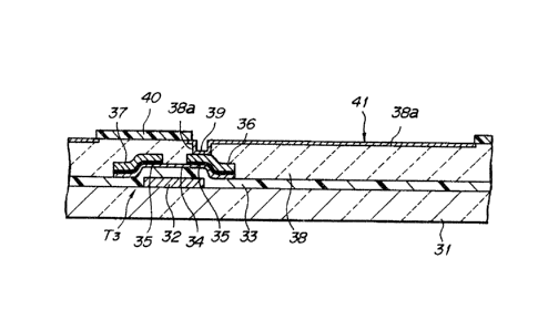
Fig. 1 shows a sectional structure of a part of
thin film transistor panel. In Fig. 1, reference symbol
T3 denotes an inverted stagger type thin film transistor
formed on transparent substrate 31. The description as
to thin film transistor T3 is omitted since it has the
same construction as that is formed in the conventional
thin film transistor panel. Reference numeral 38
denotes a transparent insulating film which is formed
over transparent substrate 31 on which thin film tran-
sistor T3 has been formed. Insulating film 38 is formed
substantially all over the surface of substrate 31 and
has a substantially flat surface. Transparent insu-
lating film 38 is made of a transparent insulating
material such as SOG (spin On Glass), into which a metal
can be diffused and which is set to almost 1 ~m in
thickness. Contact hole 39 corresponding to source
electrode 36 of thin film transistor T3 is provided in
transparent insulating film 38. Contact hole 39 is a
bottomed hole which does not reach the upper surface of
electrode 36. The bottom of contact hole 39 is almost
1 31 3563
400 ~ in thickness. Reference numeral 40 denotes a dif-
fusion preventive film which is formed on transparent
insulating film 38 except for pixel electrode forming
area where contact hole 39 is included. Diffusion pre-
ventive film 40 is provided so as to limit the diffusionarea at the time when metal-diffused layer 38a,
described later in detail, is formed by diffusing a
metal into transparent insulating film 38. Therefore,
diffusion preventive fllm 40 is made of the insulating
material, e.g., SiN, into which it is difficult to dif-
fuse a metal. Transparent metal-diffused layer 38a
which is made by diffusing conductive metal made of ITO
into transparent insulating film 38a is formed on the
area in transparent insulating film 38 without diffusion
preventive film 40. That is the layer 38a is formed on
pixel electrode forming area including contact hole 39
all over the upper surface of transparent insulating
film 38 and the inner surface of contact hole 39.
Metal-diffused layer 38a on the upper surface of
transparent insulating film 38 is used as transparent
pixel electrode 41. This transparent pixel electrode 41
is connected to source electrode 36 of thin film tran-
sistor T3 by means of metal-diffusion layer 38a depo-
sited on the inner surface of contact hole 39. In
addition, metal-diffused layer 38a (diffusion depth to
transparent insulating film 38) (almost 500 R) is
slightly thicker than the bottom of contact hole 39
1 3 1 3563
- 12 -
(almost 400 A). As a result, the bottom of contact hole
39 is connected conductively to source electrode 36 of
thin film transistor T3 because the whole thickness acts
as metal-diffused layer 38a.
A manufacturing method of the thin film transistor
panel, part of which is shown in Fig. 1, is described as
follows. First, thin film transistors T3 are formed on
transparent substrate 31 and then transparent insulating
film tSOG film) 38 is formed by applying SOG on sub-
strate 31 by almost 1 ~m in thickness and burning it, as
shown in Fig. 2A. Bottomed contact holes 39 correspond-
ing to source electrodes 36 is formed by etching trans-
parent insulting film 38. The bottom is almost 400 A in
thickness. Then, SiN is deposited on transparent
insulating film 38 by means of plasma CVD process. Then
diffusion preventive films (SiN films) 40 are formed by
patterning the deposited SiN film, as shown in Fig. 2B.
Films 40 cover transparent insulating film 38 except for
the pixe]. electrode forming areas including contact holes
39. Then, ITO film 42 is deposited by sputtering ITO on
diffusion preventive films 40 and transparent insulating
film 38 and the inner surfaces of contact holes 39, as
shown by a chain line in Fig. 2C. The ITO sputtering
is performed at the substrate temperature of almost
300C. When ITO sputtering is performed, ITO film 42
is being deposited all over the upper surface of trans-
parent insulating film 38 and the whole inner surfaces of
1 31 3~63
- 13 -
contact holes 39 and, at the same time, deposited ITO iS
being heat diffused into transparent insulating film 38
in the area uncovered by diffusion preventive film 40.
~s a result, metal-diffused layers 38a into which ITO is
diffused are formed all over the upper surface of trans-
parent insulating film 38 and the whole inner surfaces
of contact holes 39, as shown in Fig. 2C. Since diffu-
sion preventive films 40 are made of SiN into which a
metal is difficult to be diffused, ITO diffusion into
diffusion preventive films 40 scarcely occur. The ITO
sputtering is performed to the level that the ITO
diffusion depth in the bottoms of contact holes 39 for
transparent insulating film 38 are in excess of the bot-
tom thickness of contact holes 39 (almost 500 A). Metal-
diffused layers 38a which are formed on the surface oftransparent insulating film 38 are used as transparent
pixel electrodes 41 as they are, since metal-diffused
layers 38a are transparent. Metal-diffused layers 38a
formed in the inner surfaces of contact holes 39 are
also used as the contact layers which connect trans-
parent pixel electrodes 41 to source electrodes 36 of
thin film transistors T3. In this case, when heat
treatment for heating again substrate 31 at almost 300C
is executed after ITO was diffused into transparent
insulating film 38 by ITO sputtering, ITO can be
diffused into transparent insulating film 38 more deeply
so that conduction between metal-diffused layers 38a
1 3 1 3563
- 14 -
which are formed in the inner surface of contact holes
39 and source electrodes 36 of thin film transistors ~3
can be obtained more certainly.
After this process, ITO film 4~ is removed with
etching liquid including components HC~ :HNO3 :H2O =
1 : 0.08 : 1 at the temperature 35~C. Thereby pixel
electrodes 41 are obtained. As a result, thin film
transistor panel shown in Fig. 1 is completed. In this
etching process whole ITO film is removed by etching.
However, since metal-diffused layers 38a remain without
being etched, conductivity of pixel electrodes 41 and
the inner surfaces of contact holes 39 (parts of metal-
diffused layers 38a) are kept. More specifically,
Fig. 3 shows the relationship between etching time and
change in resistance values on the areas of transparent
insulating film 38 and diffusion preventive film 40 upon
whole surface etching. The surface areas of transparent
insulating film 38 recover their insulation property by
etching for about two minutes. At the time, the surface
areas of transparent insulating film 38 have a conduc-
tivity of several KQ.
In this embodiment, diffusion preventive films 40
on transparent insulating film 38 are left as they are.
However, diffusion preventive films 40 may be removed
after the completion of the TFT panel. When diffusion
preventive films 40 are left, they may be used as light
shielding films for channel portions of thin film
1 31 3563
- 15 -
transistors T3 if diffusion preventive films 40 are made
of opaque films. In addition, diffusion preventive
films 40 which limit the metal diffusion areas on
transparent insulating films 40 are made of SiN films in
this embodiment. However, diffusion preventive films 40
are not restricted to SiN films if a metal is difficult
to be diffused in the films.
However, in the thin film transistor panel
described above, metal-diffused layers 38a deposited on
the surface of transparent insulating film 38 are used
as transparent pixel electrodes 41 by diffusing a con-
ductive metal (ITO) in the surface areas of transparent
insulating film 38 and the inner surfaces of contact
holes 39. Also transparent pixel electrodes 41 are
connected to source electrodes 36 of thin film transis-
tors T3 by means of metal-diffused layers 38a on the
inner surfaces of contact holes 39. As a result,
transparent pixel electrodes 41 on transparent insulat-
ing film 38 can be connected to source electrodes 36 of
thin film transistors T3 without filling a contacting
metal in contact holes 39. Further, according to the
thin film transistor panel described above, transparent
pixel electrodes 41 and layers connecting transparent
pixel electrodes 41 to source electrodes 36 can be
formed at the same time in the surface areas of trans-
parent insulating film 38 and the inner surfaces of
contact holes 39 by diffusing conductive metal in the
- 16 - l 31 3563
surface areas of transparent insulating film 38
and the inner surfaces of contact holes 39. AS
result, formation of transparent pixel electrodes 41
and connections between pixel electrodes 41 and
source electrodes 36 of thin film transistors T3 can be
accomplished at the same time. According, the thin film
transistor panel of the present invention can be easily
obtained.
In the embodiment, the bottomed holes are provided
in transparent insulating film 38 as contact holes 39,
and metal-diffused layers 38a on the bottoms of contact
holes 39 are connected conductively to source electrodes
36 of thin film transistors T3. However, it is possible
to form contact hole 39 as a through hole which reaches
the surface of source electrode 66, as shown in Fig. 4.
In Fig. 4 since the lower surface of metal-diffused
layer 67 which is diffused throughout the inner surface
of contact hole 68 is contacted conductively to source
electrode 66, transparent pixel electrode 70 made of
metal-diffused layer 67 on transparent insulating film
69 can also be connected to source electrode 66 of thin
film transistor T3. Furthermore, although transparent
insulating films 3 8 is made of SOG in said embodiment,
it is not limited to SOG if a metal can be diffused into
the film. Also conductive metal which is diffused into
transparent insulating film 38 is not limited to ITO if
metal-diffused layers 38a can be used as transparent
,
- 17 - l 3 1 3 5 6 3
conductive films.
Another embodiment of the present invention will be
described below. Referring to Fig. 5, reference numeral
71 denotes a transparent substrate which is made of a
5 glass plate, and the like. A lot of thin film tran-
sistors T4 are aligned on substrate 71 in row and column
directions. Each of thin film transistor T4 is composed
of gate electrode G formed on substrate 71, transparent
gate insulating film 72 made of SiN and the like, i-a-Si
semiconductor film 73 formed opposite to gate electrode
G on gate insulating film 72, source and drain electro-
des S and D formed over semiconductor film 7 3 through
n+-a-Si contact layer 74. Gate insulating film 72 is
formed on gate electrode G and substantially all over
15 the substrate 71. Gate electrodes G are connected to
the unshown gate lines which are formed on substrate 71,
and drain electrodes D are connected to the unshown data
lines which are formed on gate insulating film 72. In
Fig. 5, reference symbol _ denotes a transparent pixel
20 electrode which is formed on gate insulating film 72
correspondingly to thin film transistor T4. On end
portion of pixel electrode _ is connected to source
electrode S of thin film transistor T4. Transparent
pixel electrode A is formed by forming SOG (spin On
25 Glass) film 75 on substrate 71 on which thin film
transistor T4 has been formed, and diffusing a
conductive metal in a predetermined area of SOG film 75
1313563
- 18 -
(pixel electrode area). SOG film 75 covers the whole
upper surface of thin film transistor T4 and gate
insulating film 72. The upper surface except for the
area of pixel electrode A on SOG film 75 is covered by
5 transparent upper insulating film 76 of SiN.
A manufacturing method of the thin film transistor
panel will be described below. First, thin film tran-
sistor T4 are formed on transparent substrate 71 and then
SOG film (SiO2 film) 75 is formed thereon by applying
silanol resin by means of spin coat process etc. and
burning it, as shown in Fig. 6A. Upper insulating film
76 made of SiN is formed by means of plasma CVD process
thereon. Then, upper insulating film 76 is patterned by
means of dry etching using CF4 gas to thus remove upper
15 insulating films 76 corresponding to pixel electrodes _,
as shown in Fig. 6B . Conductive metal 77 such as In, Cr
is deposited by means of sputtering or evaporation pro-
cess on upper insulating films 76 and exposed portions
of SOG film 75 as shown in Fig. 6C. Conductive metal 77
on SOG film 75 is then diffused into SOG film 75 by
heating it at almost 300C for one or two hours. When
conductive metal 77 is diffused into SOG film 75, the
metaldiffused portions of SOG film 75 become conductive
so that such metal-diffused portions of SOG film 75 can
25 be used as transparent pixel electrodes _. Since
diffused areas of conductive metal 77 on SOG film 75 are
restricted by upper insulating films 76, conductive
1313563
- 19 -
metal 77 can be diffused only in the areas which form
pixel electrodes _ of SOG film 75. As a result, pixel
electrodes A can be formed in high pattern accuracy.
After this, as shown in Fig. 6D, conductive metal 77 and
metal-diffused portions of SOG film 75, i.e., pixel
electrodes _ are exposed to thus complete transparent
electrode substrate.
However, since transparent pixel electrodes _ are
composed of metal-diffused portions of SOG film 75 by
diffusing conductive metal 77 in predetermined areas of
SOG film 75, a short-circuit between the electrodes due
to the insufficient etching and damages to the substrate
surface when forming the transparent electrode by etch-
ing the ITO film, can be prevented. In addition, since
SOG film 75 can be formed by means of spin coat process
etc. SOG film 75 can be deposited with sufficient
thickness on the stepped portions between gate insulat-
ing films 72 and source electrodes S of thin film
transistors T4. As a result, even if there are stepped
portions, on the surface of gate insulating film 72,
corresponding to transparent pixel electrodes A,
transparent electrodes _ on the stepped portions may not
be cut because the conductive layers are formed by dif-
fusing a metal in a predetermined areas of SOG film 75.
In addition, upper insulating films 76 are left on
SOG film 75 as it is so as to limit metal-diffused areas
on SOG film 75 in said embodiment. However, upper
1 3 1 3563
- 20 -
insulating films 76 may be removed together with conduc-
tive metal 77 after metal 77 is diffused in SOG film 75
and also, when leaving upper insulating films 76, they
can be used as light shielding films by making upper
insulating films 76 by opaque insulating films.
Further, an active matrix type liquid crystal display
device was described in said embodiment. However, the
present invention can be applicable to simple matrix
type liquid crystal display device or transparent
electrode substrate for transparent touch input panel.
According to the embodiments described above, pixel
electrodes are formed by diffusing a metal into the
insulating film which is formed on the thin film tran-
sistors. However, the present invention is not limited
to the embodiments. The pixel electrodes may be
formed on the surface identical to the surface on which
thin film transistors are formed or under the surface on
which thin film transistors are formed.
That is, Fig. 7 shows still another embodiment
according to the present invention, wherein the pixel
electrodes are formed on the surface identical to the
surface on which thin film transistors are formed.
Referring to Fig. 7, reference numeral 91 denotes
a transparent substrate made of glass plate etc. A lot
of inverted stagger type thin film transistors T5 are
aligned on substrate ~1 in row and column directions.
Each thin film transistor T5 is composed of gate
''` ..,,,. - -
1 3 1 3563
- 21 -
electrode G formed on substrate 91, gate insulating film
92 made of SiN etc. and formed on gate electrode G,
i-a-Si semiconductor film 93 formed on gate insulating
film 92 opposite to gate electrode G, n+-a-Si layer 94
which forms source and drain areas and formed on semi-
conductor layer 93, source and drain electrodes S and D
which are formed over n+-a-Si layer 94 through contact
metal layer 95. Gate electrode G is connected to the
unshown gate line formed on substrate 91, and drain
electrode D is connected to the unshown data line formed
on gate insulating film 92.
In Fig. 7, reference numeral 96 denotes a SOG film
which is formed on transparent substrate 91. SOG film
96 is formed substantially all over substrate 91 except
for the areas of gate electrode G and gate line of thin
film transistor T5. Gate lnsulating film 92 of thin
film transistor T5 is formed substantially all over
substrate 91 on SOG film 96. Opening 92a for exposing
the surface of SOG film 96 is provided in gate insu-
lating film 92 so as to coincide with the pattern oftransparent pixel electrode 96a corresponding to thin
film transistor T5. Conductive metal such as Sn, In, ITO
is diffused into the exposed area in opening 92a of gate
insulating film 92 at a depth of almost 100 ~ from the
surface of SOG film. Metal-diffused area of SOG film 96
is used as transparent pixel electrode 96a which has a
conductivity by metal diffusion. The outer end of
1313563
- 22 -
source electrode S is overlapped on the edge portion of
transparent pixel electrode sça and is thus connected to
pixel electrode 96a. In Fig. 7, reference numeral 97
denotes a transparent protective insulating film which
is made of SiN etc. and covers thin film transistor T5
and pixel electrode 96a.
A manufacturing method of the thin film transistor
of Fig. 7 will be describe below. First, gate
electrodes G which are lower electrodes of inverted
stagger type thin film transistors T5, and gate lines
are formed by depositing metal film such as Cr, Ti on
transparent substrate 91 and then pattering it. Then,
SOG film (SiO2 film) 36 is formed on substrate 91 by
applying silanol resin by means of spin coat etc. all
over substrate 91 and burning it. SOG film 96 is made
flat to substantially identical level to gate electrodes
G, as shown in Fig. 8A, by etching SOG film 96 back so
as to expose the surface of gate electrodes G. As shown
in Fig. 10B, gate insulating film (SiN film) 92, i-a-Si
semiconductor layer 93, n+-a-Si layer 94, and contact
metal layer 95 made of Cr, Ti etc. are deposited in
serial by means of plasma CVD process, sputtering pro-
cess and the like. Then, contact metal layer 95,
n+-a-Si layer 94 and i-a-Si semiconductor layer 93 are
patterned to the shapes of the transistor devices, as
shown in Fig. 8C. Openings 92a for exposing pixel
electrode forming areas on SOG film 96 are formed in
~313563
- 23 -
gate insulating film 92, as shown in Fig. 8D, by etching
predetermined areas (pixel electrode forming areas) of
gate insulating film 92 correspondingly to patterns of
pixel electrodes s6a by means of dry etching using CF4
gas. Openings 92a can be formed in high pattern
accuracy due to easiness of etching of gate insulating
film (SiN film) 92.
As shown in Fig. 8E, conductive metal _ is de-
posited by means of sputtering or evaporation process.
The metal A is made of Sn, In, ITO etc. and used as
-
source and drain electrodes S and D. After this, con-
ductive metal A is diffused into surface areas of SOG
film 96 which are exposed in openings 92a by means of
heat treatment. Metal A is heated for two or three
hours at the temperature of almost 300C. Where,
"diffusion" means that metal molecules get into molecu-
lar clearances of SOG fllm 96. Conductive metal A is
diffused into SOG film 96 from the surface at a depth of
almost 100 A by means of the heat treatment. In
Fig. 8E, reference numeral 96a denotes metal-dlffused
areas of SOG film 96, and the areas 96a can be used as
the transparent pixel electrodes as they are. Since
transparent pixel electrodes (metal-diffused areas of
SOG film 96) 96a are formed by limiting diffusible areas
of conductive metal _ into SOG film 96 by means of gate
insulating film 92, the patterns of the pixel electrodes
correspond to the shapes of openings 92a on gate
1 31 3563
- 24 ~
insulating film 92. Therefore pixel electrodes s6a can
be formed in high pattern accuracy. Then, as shown in
Fig. 8F, source electrodes S, drain electrodes D and
data lines are formed by patterning the film of conduc-
tive metal _. The outer portions of source electrodes Sare overlapped on the side edge portions of pixel
electrodes 96a. At that time, undesired portions of
contact metal layers 95 and n-a-Si layers 94 between
source and drain electrodes S and D are removed by
etching. As a result, thin film transistor T5 have been
completed and then film transistor panel shown in Fig. 7
has been completed by forming protective insulating film
97.
More specifically, according to the thin film tran-
sistor panel described above, the metal-diffused areas
of SOG film 96 can be used as transparent pixel
electrodes 96a by diffusing conductive metal _ into pre-
determined areas of SOG film 96 so as to give the areas
conductivity. Pixel electrodes 96a can be obtain in
high pattern accuracy by masking areas of SOG film 96
except for the areas corresponding to the pixel
electrodes by gate insulating films 92 and then diffusing
conductive metal _ thereon. As a result, dimensional
accuracy as to transparent pixel electrodes 96a can be
obtained highly. Accordingly, high density display can
be achieved by making pixel electrodes 96a minutely. In
addition, in this embodiment, since gate insulating film
1 31 3563
- 25 -
92 is used as a mask for limiting metal diffused areas
of SOG film 96 ad since metal A which forms source and
drain electrodes S and D are diffused into SOG film 96,
thin film transistor panel can be made efficiently by
few steps and at low cost.
In said embodiment, metal A corresponding to source
and drain electrode S and D is used as a conductive
metal which is diffused in SOG film 96. However, such
conductive metal may be formed by other metals. In this
case, after conductive metal is deposited on SOG film 96
and is diffused into SOG film 96 by heat treatment,
source and drain electrodes S and D may be formed and
then the deposited metal is removed by etching process.
Gate insulating film 92 is used as a mask for limiting
metal diffused areas on SOG film 96 is said embodiment.
However, the mask may be formed by photoresist process
etc.. In this case, conductive metal can be diffused
into SOG film 96 at any time in the course of
manufacturing steps of the thin film transistor panel.
Furthermore, the thin film transistors are made of
inverted stagger type transistors. However, the thin
film transistors may be composed of inverted coplanar
type or stagger type transistors. When stagger type
transistors are applied as the thin film transistors,
a metal corresponding to source and drain electrodes or
other conductive metal may be diffused into SOG film to
make transparent pixel electrodes in a similar manner to
1313563
- 26 -
said embodiment. When an inverted coplanar type tran-
sistor is applied, a metal corresponding to gate
electrodes or other conductive metal may be diffused
into SOG film to make transparent pixel electrodes.
When stagger transistors are applied as the thin film
transistors, since the lower electrodes, i.e., source
and drain electrodes are formed on the transparent
substrate, transparent pixel electrodes and the source
electrodes of thin film transistors can not be formed
overlappingly. The transparent pixel electrodes are
formed by diffusing the conductive metal into the SOG
film which is formed on the substrate except for the
source and drain electrode areas. However, when parts
of conductive metal formed on the SOG film are left with
extending over pixel and source electrodes so as to
diffuse a metal into SOG film, the conductive metal
can connect pixel electrodes and source electrodes
conductively and firmly.
Fig. 9 shows still another embodiment of the
present invention wherein the pixel electrodes are
formed under the surface on which thin film transistors
are formed. In Fig. 9, reference numeral 111 denotes a
transparent substrate made of glass plate etc.. SOG
film 112 is formed on substrate 111 substantially all
over the surface 111. A lot of inverted stagger type
thin film transistors T6 are aligned on SOG film 112 in
row and column directions. Each of thin film transistor
1313563
T6 is composed of gate electrode G formed on SOG film
112, gate insulating film 113 made of SiN etc. and
formed on gate electrode G, i-a-Si semiconductor film
114 formed on gate insulating film 113 opposite to gate
electrode G, n+-a-Si layer 115 which forms source and
drain areas and is formed on semiconductor layer 114,
and source and drain electrodes S and D which are formed
over n+-a-Si layers 115 through contact metal layers
116. Gate electrode G is connected to the unshown gate
line formed on SOG film 112, and drain electrode D is
connected to the unshown data line formed on gate
insulating film 113.
Gate insulating film 113 is formed substantially
all over SOG film 116. Openings 113a for exposing the
surfaces of SOG film 112 are provided in gate insulating
film 113 so as to coincide with the patterns of transpar-
ent pixel electrodes 112a corresponding to thin film
transistor T6. Conductive metal such as Sn, In, ITO is
diffused into the exposed areas in openings 113a of gate
insulating film 113 at a depth of almost 100 ~ from the
surface of SOG film. Metal-diffused areas of SOG film
112 is used as transparent pixel electrodes 112a which
have conductivity by metal diffusion. The outer end of
source electrode S of thin film transistor T6 is
overlapped on the edge portion of transparent
pixel electrode 112a and is thus connected to the pixel
electrode 112a. In Fig. 9, reference numeral 117
1 31 3563
- 28 -
denotes a transparent protective insulating film which is
made of SiN etc. and covers thin film transistors T6 and
pixel electrode 112a.
A manufacturing method of the thin film transistor
panel will be described below. First, SOG film (SiO2
film) 112 is formed on substrate 111 by applying silanol
resin by means of spin coat process etc. all over
transparent substrate 111 and burning it, as shown in
Fig. 10A. Then, a gate electrode G and gate lines are
formed by means of depositing a metal film such as Cr,
Ti on SOG film 112 and patterning it. As shown in
Fig. 10B, gate insulating film (SiN film ) 113, i-a-Si
semiconductor layer 114, n+-a-Si layer 115, and contact
metal layer 116 made of Cr, Ti etc. are deposited
serially by means of plasma CVD process, sputtering
process and the like. Then, contact metal layer 116,
n+-a-Si layer 115 and i-a-Si semiconductor layer 114 are
patterned to the shape of the transistor devices, as
shown in Fig. 10C. Openings 113a for exposing pixel
electrodes forming areas on SOG film 112 are formed in
gate insulating film 113, as shown in Fig. 10D, by
etching predetermined ar~as (pixel electrode forming
areas) of gate insulating film 113 correspondingly to
patterns of pixel electrodes 112a by means of dry etching
using CF4 gas. Openings 113a can be formed in high
pattern accuracy due to easiness of etching of gate
insulating film (SiN film) 113.
1 3 ~ 3563
- 29 -
As shown in Fig. 12E, conductive metal A is depo-
sits by means of sputtering or evaporation process. The
metal _ is made of Sn, In, ITO etc. and used as source
and drain electrode S and D. After this, conductive
metal A is diffused into areas of SOG film 112 which are
exposed in openings 113a on gate insulating film 113, by
means of heat treatment. Metal _ is heated for two or
three hours at the temperature of almost 300C. Where,
"diffusion" means that metal molecules get into
molecular clearances of SOG film 112. Conductive metal
_ is diffused into SOG film 112 the surface at a depth
of almost 100 ~ by means of the heat treatment. In
Fig. 10E, reference numeral 112a denotes metal-diffused
areas of SOG film 112, and the areas 112a can be used as
the transparent pixel electrode as they are. Since
transparent pixel electrodes (metal-diffused areas of
SOG film 112) 112a are formed by limiting diffusible
areas of conductive metal A into SOG film 112 by means
of gate insulating film 113, the patterns correspond to
the shapes of openings 113a on gate insulating film 113.
Therefore, pixel electrodes 112a can be formed in high
patter accuracy. Then, as shown in Fig. lOF, source
electrodes S, drain electrodes D and the data lines are
formed by patterning the film of conductive metal A.
The outer portion of source electrodes S are overlapped
on the side edge portions of pixel electrodes 112a. At
that time, undesired portions of contact metal layer 116
1 3 1 3563
- 30 -
and n+-a-Si layer 115 between source and drain elec-
trodes S and D are removed by etching. As a result,
thin film transistor T6 has been completed and thin film
transistor panel shown in Fig. 9 has been completed by
forming protective insulating film 117.
More specifically, according to the thin film tran-
sistor panel described above, the metal-diffused areas
of SOG film 112 can be used as transparent pixel elec-
trodes 112a by diffusing conductive metal A into a
predetermined areas of SOG film 112 so as to give the
areas conductivity. Pixel electrodes 112a can be obtain
in high pattern accuracy by masking areas of SOG film
112 except for the areas corresponding to the pixel
electrodes by gate insulating film 113 and then diffus-
ing conductive metal _ thereto. As a result, as in theembodiment shown in Fig. 9, dimensional accuracy as to
transparent pixel electrodes 112a can be obtained
highly. Accordingly, high density display can be
achieved by masking pixel electrodes 112a minutely.
Since the thin film transistors are formed by forming
SOG film 112 on transparent substrate 111 and forming
thin film transistors T6 and gate lines thereon, even if
transparent substrate 111 has damages thereon, the
damages on the substrate are buried by SOG film 112.
Therefore, the disconnections of gate and data lines due
to the damages on substrate 111 can be prevented. In
addition, in this embodiment since gate insulating film
1 31 3563
- 31 -
113 is used as masks for limiting the metal-diffused
areas of SOG film 96 and since metal A which forms
source and drain electrodes S and D ar0 diffused into
SOG film 96, thin film transistor panel can be made
efficiently by few steps and at low cost.
Furthermore, the thin film transistors are made of
inverted stagger type transistors. However, the thin
film transistors may be composed of inverted coplanar
type, coplanar type, or stagger type transistors.
Fig. 11 shows another embodiments of the present
invention. The thin film transistor panel of this
embodiment is made of inverted coplanar type transis-
tors. The thin film transistor panel is constructed by
forming SOG film 132 on transparent substrate 131,
forming ground insulating film 138 such as SiN which
also acts as a mask for limitlng the metal-diffused
areas on SOG film 132 thereon, then forming inverted
coplanar type thin film transistor T7 on ground
insulating film 138. Transparent pixel electrodes 132a
are formed by diffusing a conductive metal in the
exposed areas in openings 138a which are formed on the
ground insulating film 138a correspondingly to the
patterns of the pixel electrodes. Incidentally, the
description as to the construction of the inverted
coplanar type thin film transistors is omitted since
only the layer construction as to the alectrodes and the
semiconductor layers are different.
1 31 3563
The thin film transistor panel is manufactured by
the following steps. First, as shown in Fig. 12A, SOG
film 132 is formed on transparent substrate 131 and then
ground insulating film (SiN film) 138 is formed thereon.
After this, gate electrodes G and gate liens (not shown)
are formed. Then, as shown in Fig. 12B, gate insulating
film (SiN film~ 133 is formed, and openings for exposing
the pixel electrode areas of SOG film 132 are formed in
gate insulating film 133 and in ground insulating film
138. Conductive metal _ and n+-a-Si layer corresponding
to source and drain electrodes S and D are deposited as
shown in Fig. 14C and then heat treatment is performed
so as to diffuse conductive metal _ into the pixel
electrode areas of SOG film 132. As a result, transpar-
ent pixel electrodes 132a are obtained. Then, as also
shown in Fig. 14C, n+-a-si layer 135 and the film of
conductive metal _ are patterned so as to from source
and drain electordes S and D and data lines (not shown).
At that time, conductive metal A and n+-a-Si layer 135
which are deposited on pixel electrodes 132a are left
without being removed. The reason why conductive metal
_ on pixel electrodes 132a are left is that pixel
electrodes 132a may be prevented from being deleted by
etching at the time of patterning i-a-Si semiconductor
layer 134. As shown in Fig. 12D, i-a-Si semiconductor
layer 134 is deposited. Layer 134 and n+-a-Si layer 135
are patterned by wet or dry etching, and then conductive
1 31 3563
- 33 -
metal A on pixel electrodes 132a are removed by etching
as shown in Fig. 12E with leaving the areas of source
electrodes S which are overlapped on the edge portions
of pixel electrodes 132a. AS a result, the thin film
transistors T7 are constructed and the thin film tran-
sistor panel in Fig. 11 is completed by forming protec-
tive insulating film 137.
In this embodiment, the metal-diffused areas of SOG
film 132 can be used as transparent pixel electrodes
132a by diffusing conductive metal A into predetermined
areas of SOG film 132 formed on transparent substrate
131. Pixel electrodes 132a can be obtained in high
pattern accuracy. In this embodiment, SOG film 132 and
ground insulating film 138 are formed as two layers on
transparent substrate 131, and thin film transistors
T7 and gate and data lines are formed thereon. As a
result, even if transparent substrate 131 has consid-
erably deep damages on the surface, the surface of thin
film transistors T7 (surface of ground insulating film
138) becomes flat. Therefore, the disconnections of
gate and data lines due to the damages on substrate 131
can be prevented.
Fig. 13 shows another embodiments of the present
invention. In this embodiment the thin film
transistor panel comprises coplanar type transistors.
The thin film transistor panel is constructed, as shown
in Fig. 13, by forming SOG film 152 on transparent
1 31 3563
- 34 -
substrate 151, forming ground insulating film 158 such
as SiN which also acts as a mask for limiting the metal-
diffused areas on SOG film 152 thereon, then forming
coplanar type thin film transistors T8 on ground
insulating film 158. Transparent pixel electrodes 152a
are formed by diffusing a conductive metal in exposed
areas in openings 158a which are formed in the ground
insulating film 158 correspondingly to the patterns of
the pixel electrodes. Incidentally, the descriptions as
to the construction of the coplanar type thin film
transistors T8 is omitted since the layer construction
as to the electrodes and semiconductor layers are formed
only reversely.
The thin film transistor panel is manufactured by
the following steps. First, as shown in Fig. 14A, SOG
film 152 is formed on transparent substrate 151 and then
ground insulating film (SiN film) 158, i-a-Si semicon-
ductor layer 154, n+-a-Si layer 155 and contact metal
layer 156 are formed thereon serially. After this, as
shown in Fig. 14B, contact metal layer 156, n+-a-Si
layer 155 and i-a-Si semiconductor layer 154 are
patterns to the shapes of transistor devices. Then,
openings 158a for exposing pixel electrode areas of SOG
film 152 are formed in ground insulating film 158.
Conductive metal _ corresponding to source and drain
electrodes S and D are deposited as shown in Fig. 14C.
Then heat treatment is performed so as to diffuse
1 31 3563
conductive metal _ into the pixel electrode areas of SOG
film 152. As a result, transparent pixel electrodes
152a are obtained. Then, as shown in Fig. 14D, the film
of conductive metal _ is patterned so as to form source
and drain electrodes S and D and data lines. The outer
portions of source electrode S are overlapped on the
side perlpheral portions of pixel electrodes 152a. At
the same time, undesired portions of contact metal layer
15~ and n+-a-Si layer 155 are removed by etching. Gate
insulating film (SiN film) 153 which acts also as pro-
tective insulating film is formed. Gate electrodes G and
the gate lines are formed on gate insulating film 153 to
thus complete thin film transistors T8. Accordingly,
thin film transistor panel in Fig. 13 is completed.
Fig. 15 shows another embodiments of the present
invention. In this embodiment, the thin film transistor
panel comprises the stagger type transistors. The thin
fllm transistor panel is constructed, as shown in
Fig. 15, by forming SOG film 172 on transparent sub-
strate 171, forming ground insulating film 178 such as
SiN which also acts as a mask for limiting the metal-
diffused areas on SOG film 172 thereon, then forming
coplanar type thin film transistors T9 on ground
insulating film 178. Transparent pixel electrodes
172a are formed by diffusing a conductive metal in the
exposed areas in openings 178a which are formed on the
ground insulating film 178 correspondingly to the
1 31 3563
- 36 -
patterns of the pixel electrodes. The descriptions as
to the construction of the stagger type thin film
transistors Ts is omitted since the layer construction
as to the electrodes and semiconductor layer are formed
only reversely in comparison with the inverted stagger
type transistors.
The thin film transistor panel is manufactured by
the following steps. First, as shown in Fig. 16A, SOG
film 172 is formed on transparent substrate 171 and then
ground insulating film (SiN film) 178 is formed thereon.
After this, openings 178a for exposing the pixel
electrode areas of SOG film 172 are formed on ground
insulating film 178. As shown in Fig. 16B, conductive
metal _ and n+-a-Si layer 175 corresponding to source
and drain electrodes S and D are deposited. Then heat
treatment is performed so as to diffuse conductive metal
_ into the pixe~ electrode areas of SOG film 172. As a
result, transparent pixel electrodes 172a are obtained.
Then, as shown in Fig. 16C, the film of conductive metal
A and n+-a-Si layer 175 are patterned so as to form
source and drain electrodes S and D and data lines. At
that time, conductive metal _ and n+-a-Si layer 175
which are deposited on pixel electrodes 172a are left
without being removed. Then, i-a-Si semiconductor
layer 174 and gate insulating film (SiN film) 173 are
deposited. Gate insulating film (SiN film) 173, i-a-Si
semiconductor layer 174 and n+-a-Si layer 175 are
1 3 1 3563
- 37 -
patterned to the shapes of transistor devices, as shown
in Fig. 16D. Conductive metal _ on pixel electrodes
172a is removed by etching as shown in Fig. 16E with
leaving the areas of source electrodes S which are
overlapped on the edge portion of pixel electrodes 172a
and, at that time, gate electrodes G and gate lines are
formed on gate insulating film 173. AS a result, the
thin film transistors T9 are constructed and the thin
film transistor panel in Fig. 15 is completed by forming
protective insulating film 177.
In the embodiments in Figs. 13 and 15, the metal-
diffused areas of SOG film can be used as transparent
pixel electrodes by diffusing conductive metal _ into
predetermined areas of SOG film. Pixel electrodes can
be obtained in high pattern accuracy. In this embodi-
; ment, SOG film is formed on transparent substrate, and
thin film transistors and gate and data lines are formed
thereon. As a result, even if transparent substrate has
damages on the surface, the disconnections of gates and
data lines due to the damages on substrate can be surelyprevented.
In said embodiments, metal _ corresponding to source
and drain electrodes S and D is used as a conductive
metal which is diffused in SOG film. However, such
conductive metal may be formed by other metals. In this
case, after conductive metal is deposited on SOG film
and is diffused into SOG film by heat treatment, source
1 31 3563
- 38 --
and drain electrodes S and D may be formed and then the
deposited metal is removed by etching process. When
coplanar type or stagger type transistors are used as
thin film transistors, it is possible to use the same
metal as the gate electrode G which is diffused into the
SOG film. In this case, firstly openings for exposing
the areas for the pixel electrodes on SOG film are formed
in the gate insulating film, then conductive metal
corresponding to gate electrode G and gate lines are
deposited thereon. The conductive metal can be diffused
by heat treatment thereafter. The gate insulating film
and the ground insulating film are used as a mask for
limiting metal diffused areas on SOG film in said
embodiment. However, the mask may be formed by photo-
resist process etc. In this case, conductive metal canbe diffused into SOG film at any time in the course of
manufacturing steps of the thin film transistor panel.
The thin film transistor panel of the present
invention described above will be used as a liquid
crystal display device in which the opposing substrate
for interposing a liquid crystal thersbetween as shown in
Fig. 17. More specifically, gate lines 192 and drain
lines 193 are aligned in a matrix form on transparent
insulating substrate 191 and thin film transistors 194
are arranged at crossing portions. Since the thin
film transistors have the same construction as the
transistors described above, it is shown as an equivalent
1 3 1 3563
- 39 -
circuit. Pixel electrodes 196 are connected to source
electrodes 195 of thin film transistors 194. Pixel
electrodes 196 are not shown, but are formed by diffus-
ing predetermined areas of diffusible insulating film
which covers gate lines 192, drain lines and thin film
transistors 194. Pixel electrodes 196 are arranged
respectively a plurality of areas surrounded by gate
lines 192 and drain lines 193 and are separated
electrically each other. The outer shapes of pixel
electrodes 196 are formed ad;acent to gate lines 192 and
drain lines 193. As described in the embodiments, pixel
electrodes 196 and source electrodes 195 are connected
directly or through contact holes. Transparent opposing
substrate 198 on which transparent electrodes 197 are
formed is arranged opposite to the thin film transistor
panel, and a liquid crystal 199 is interposed into the
substrates to thereby complete a liquid crystal display
device.
The liquid crystal display device is operated as
follows. The scanning signals are serially supplied to
a plurality of gate lines 192 and the data slgnals for
controlling the active state of the pixels are supplied
to a plurality of drain lines 193 in coincidence with
the timing of the scanning signals. When the scanning
signal is supplied to the gate electrodes 200, the thin
film transistors are turned ON, reads the data signals
supplied at that timing and supplies it to the pixel
1 31 3~63
- 40 -
electrode 196. In accordance with potential difference
applied to the opposing electrodes, electric fields
are applied to liquid crystal 199 between the pixel
electrodes to which the data signals are supplied and
transparent electrodes 197 on opposing substrate 198.
Liquid crystal 199 changes its molecular orientation
according to the electric field so as to control a
transmission and interception of light.
As described above, according to the thin film
transistor panel of the present invention, the pixel
electrodes are formed by diffusing conductive material
into predetermined areas of the diffusible insulating
film so as to give the conductivity in the areas so
that the pixel electrodes can be formed in high pattern
accuracy to obtain the minute pixel electrodes.
Accordingly, the liquid crystal display device using
the thin film transistor panel of the present invention
is able to realize an extremely high density image
display.
As described in detail, the present invention can
provide the thin film transistor panel which is able to
achieve high density display by the minute electrodes
and prevent the disconnections between gate and drain
lines, as described above, and which can be very easily
manufactured since diffusible insulating materials are
used in the thin film transistor panel and the insu-
lating materials are used as the pixel electrodes by
1 31 3563
- 41 -
diffusing them to give the conductivity.
The present inventions are not limited to the
formation of pixel electrodes. The wiring constructions
of the thin film transistor panel of the present inven-
tion are described below.
Fig. 18 is a perspective view showing an embodimetn
of a wiring connection of the thin film transistor
panel of the present invention. This embodiment can be
applied to the panel in which an inverted stagger type
transistors are used.
In Fig. 18, reference symbol 201 denotes an
insulating substrate made of a glass plate etc.; and
T10, an inverted stagger type thin film transistor which
is formed on insulating substrate 201. Reference
numeral 205 denots a transparent insulating film which
covers thin film transistors Tl0. Transparent insu-
lating fil~ 205 is made of a transparent insulating
material such as SOG (spin On Glass) into which a metal
can be diffused and which is set to almost 1 ~m in
thickness. Contact holes 206 are provided in
transparent insulating film 205 correspondingly to
source and rain electrodes S and D of thin film tran-
sistor T10. The depth of contact hole 206 reaches
source and drain electrodes S and D. Reference numeral
207 denotes a diffusion preventive film which is formed
on insulating film 205. Openings 208 are provided in
diffusion preventive film 207 correspondingly to the
1 31 3563
- 42 -
areas of contact holes of insulating film 205. The diam-
eter of opening 208 is slightly larger than the upper
diameter of contact holes 206. Diffusion preventive
films 207 are provided so as to limit the diffusion areas
at the time when metal-diffused layer 205a, described
layer in detail, are formed by diffusing a metal in
insulating film 205. Therefore, diffusion preventive
films 207 are made of the insulating material, e.g., SiN
into which a metal is difficult to be diffused. Metal-
diffused layer 205a is formed on the areas of insulatingfilm 205 without diffusion preventive film 207, i.e.,
contact hole forming areas corresponding to openings 208
in diffusion preventive film 207 and all over the inner
surfaces of contact holes and the surfaces of insulating
film 205 in the peripheral areas of the constant holes.
Metal-diffused layer 205a is made by diffusing conduc-
tive metal made of ITO into insulating film 205.
Reference numeral 209 denotes wirings which are formed
on insulating film 205 and are made of conductive metal
such as A~ etc.. Parts of wirings 209 are overlapped on
metal-diffused layers 205a in the peripheral areas of
contact holes 206 and are connected to metal-diffused
layer 205a conductivity. Reference numeral 209a denotes
a contact metal layer which are formed on the inner bot-
tom area of contact holes 206. Contact metal layers209a are made of the same metal as wirings 209 and is
contacted to source and drain elPctrodes S and D and the
1 3 1 3563
- 43 -
metal-diffused layers 205a on the inner surfaces of
contact holes 206 to thus connect conductively source
and drain electrodes S and D and metal-diffused layers
205a on the inner surface of contact holes.
Process of forming metal-diffused layers 205a,
wirings 209 and contact metal lay~rs 209a will be
described below with reference to Figs. l9A to l9C.
First, thin film transistors T10 are formed on insulat-
ing substrate 201 and then transparent insulating film
(SOG film) 205 is formed by applying SOG on substrate
201 by almost 1 ~m in thickness and duriny it, as shown
in Fig. l9A. Contact holes 206 are formed by etching
insulating film 205 correspondingly to source and drain
electrodes S and D of thin film transistors T10. Then,
SiN is deposited on insulating film 205 by means of
plasma CVD process by almost 1000 A in thickness so as
to form diffusion preventive films 207, as shown in
Fig. l9A. Openings 208 for exposing the contact holes
are formed in insulating film 205 by etching. Then, ITO
film _ is deposited by sputtering ITO as a conductive
metal which is diffused into insulating film 205 all
over the surface of insulating film 205 and the inner
surfaces of contact holes 206, as shown in by a chain
line in Fig. l9B. The ITO sputtering is performed at
the substrate temperature of almost 300C. When ITO
sputtering is performed, ITO film _ is deposited all
over the surface of insulating film 205 and the inner
1 31 3563
- 44 -
surfaces of contact holes 206 and, at the same time,
deposited ITO is heat diffused into insulating film 205
in the areas uncovered by diffusion preventive films
207. As a result, metal-diffused layers 205a into which
ITO is diffused are formed all over the surfaces in the
peripheral areas of the contact holes and the whole
inner surfaces of contact holes 206 in insulating film
205, as shown in Fig. l9B. ITO film A is also deposited
on diffusion preventive film 207 and source and drain
electrodes S and D exposed in contact holes 206.
However, since diffusion preventive films 207 are made
of SiN film into which metal is unable to diffuse, ITO
dlffusion scarcely occurs in diffusion preventive films
207 and IT0 _ deposited on source and drain electrodes S
and D is only deposited on electrodes S and D.
The ITO sputtering is performed to the level that
the ITO diffusion depth into insulating film 205, that
is, layer thickness of metal-diffused layers 205a,
becomes enough thickness (almost 500 A) as the
conductive film. In this case, after ITO was diffused
into insulating film 205 by sputtering ITO, when heat
treatment is executed to heat again substrate 201 at
almost 300~C, ITO can be diffused into insulating film
205 deeply so that layer thickness of metal-diffused
layers 205a can be obtained satisfactorily.
After this step, ITO film _ on diffusion preventive
film 207 is removed by etching 207 with etching liquid
1 31 3563
- 45 -
consisting of components HC~ : HNO3 : H2O = 1 : 0.08 : 1
at the temperature 35C. When etching is done on the
whole surface, the surfaces of diffusion preventive
films 207 made of SiN recovers its insulating property
by two minute etching so that metal-diffused layers 205a
on contact hole areas in insulating film 205 are sepa-
rated each other. In this case, both ITO films _ on
diffusion preventive film 207 and insulating film 205
are removed by etching. However, since metal-diffused
layers 205a in insulating film 205 remain without being
etched, the metal-dlffused layer forming areas of
insulating film 205 keep the conductivity of several Kn
of resistance value at the time when diffusion pre-
ventive films 207 again obtain its insulating property.
ITO films _ deposited on the bottom of contact holes
206, that is, source and drain electrodes S and D Gf
thin film transistor T10, are also removed by whole
surface etching. However, source and drain electrodes S
and D remain without being etched. The lower edge
surfaces of metal-diffused layers 205a are contacted
conductively to source and drain electrodes S and D of
thin film transistors T10. Accordingly, metal-diffused
layers 205a act as contact layers which connect source
and drain electrodes S and D of thin film transistors
T10 to wirings 209 on insulating film 205.
Conductive metal (for example, A~) is deposited by
means of plating or sputtering process, and metal film
1 31 3563
- 46 -
which corresponds to wirings 209 is formed on diffusion
preventive films 207 and insulating film 205, as shown in
Fig. l9C. AT the same time, the metal is also deposited
on the inner surfaces of contact holes 206 so as to form
contact metal layers 209a on the inner bottoms of contact
holes 206. Deposited thickness of the metal can be
selected almost twice as thick as diffusion preventive
films 207. More specifically, if the thickness of
diffusion preventive films 207 is 1000 ~, the metal will
be deposited 2000 ~ in thickness. As a result, the
metal can be deposited on the stepped portions between
the surfaces of diffusion preventive films 207 and
insulating film 205 in sufficient thickness, and the
metal film which continues from diffusion preventive
films 207 to insulating film 205 can be formed without
disconnection. When the metal is deposited to such
thickness, contact metal layers 209a deposited on contact
holes 206 are contacted to source and drain electrodes S
and D and to metal-diffused layers 205a on the inner
surfaces of contact holes 206 with sufficient areas.
Metal-diffused layers 205a which are contacted to source
and drain electrodes S and D can be more firmly and
conductivity connected to source and drain electrodes S
and D. After this, the metal film deposited on
diffusion preventive films 207 and insulating film 205
is patterned in order to form wirings 209 (source and
drain wirings), as shown in Fig. 18. The patterning of
13135~3
- 47 -
the metal film can be easily done due to thin thickness
of the metal film of almost 2000 ~ and accordingly
minute wirings 209 can also be formed.
More specifically, the wiring connection
construction is made by the following steps. Conductive
metal (ITO) is diffused into the contact hole forming
areas so as to form metal-diffused layers 205a in the
inner surface of contact holes 206 and the surfaces of
the insulating film 205 in the peripheral areas of the
contact holes. Parts of wirings 209 which are formed on
insulating film 205 are overlapped on metal-diffused
layers 205a in the peripheral areas of the contact holes
206 so as to connect conductively wirings 209 to metal-
diffused layers 205a. At the same time when the metal
corresponding to wirings 209 is deposited on insulating
film 205, the metal is deposited on the inner bottoms of
contact holes 206 so as to form contact metal layers
209a on the inner bottom of contact holes 206. As a
result, metal-diffused layers 205a on the inner surfaces
of the contact holes and source and drain electrodes S
and D are firmly and conductively connected by means of
contact metal layers 209a each other. Therefore,
according to the wring connection construction, even if
wirings 209 formed in insulating film 205 which covers
thin film transistors T10 are connected to source and
drain electrodes S and D in contact holes 206, wirings
209 are surely and conductively connected to source and
1 31 3563
- 48 -
drain electrodes S and D through conductive metal 205a,
although wirings 209 on insulating film 205 and the
metal corresponding to contact metal layers 209a in
contact holes 206 are not deposited thickly. Conductive
metal 205a is diffused into the contact hole forming
areas of insulating film 205. According to the wiring
connection construction, because deposited thickness of
the metal which corresponds to wirings 209 and contact
metal layers 209a can be made thin, deposit time of the
lo metal can be shortened. Furthermore, the patterning of
the deposited metal film corresponding to wirings 209
can be easily done and also fine wirings 209 are made
possible. Incidentally, although the connection
construction of the wirings which are connected to the
source and drain electrodes of the inverted stagger type
thin film transistor was described in the embodiment,
the present invention also can be applicable to another
transistors or ordinary transistors using Si single
crystal substrate.
Figs. 20 to 22 show the embodiments shown in Fig. 6
to 8, respectively. More specifically, Fig. 20 shows
the connection construction of the wirings 228 which are
connected to gate and drain electrodes G and D of
stagger type thin film transistor Tll. Fig. 21 shows
the connection construction of the wirings 228 which are
connected to gate and drain electrodes G and D of
coplanar type thln film transistor T12. Fig. 22 shows
1 31 3563
- 49 -
the connection construction of the wirings 228 which
are connected to source and drain electrodes S and D
of inverted coplanar type thin film transistor T13.
Incidentally, the basic constructions of the embodiments
shown in Figs. 20 to 22 are identical to that of the
embodiment shown in Fig. 5 and therefore the
descriptions are omitted.
Another embodiment of a wiring connection of the
thin film transistor panel of the present invention
will be described below. Fig. 23 is a schematic
sectional view showing another embodiment of the present
invention. Referring to Fig. 23, thin film transistor
T14 is constituted by gate electrode 252 made of Cr
etc., gate insulating layer 253 made of nitric silicon
15 etc., a-Si semiconductor layer 254 made of a-Si
(amorphous silicon)~ ohmic contact n+-a-Si layers 255 in
which n type impurity is doped at high density, and
source and drain electrodes 256 made of Cr etc. on the
insulating substrate 251 made of glass etc... Thin film
transistor T14 is covered by thick insulating film 257
which is made of SOG and is almost 1 ~m in thickness.
Contact holes 258 are opened on source and drain
electrodes 256. Furthermore, diffusion preventive
layers 259 which is made of nitric silicon is formed on
insulating film 257 by 1000 A in thickness except for
the areas of conductive layers 2510 described later.
Conductive layers 2510 are formed in almost 500 A
1 31 3563
- 50 -
thickness by diffusing a mixture of Sn, In and 2 on the
surfaces of insulating film 257 except for the areas of
diffusion preventive layers 259 and on the surfaces of
contact holes 258. More specifically, conductive layers
2510 are the wiring layers which connect source and
drain electrodes 256 to the source and drain electrodes
of other thin film transistors each other through
contact holes 258 and insulating film 257.
A method of manufacturing the wiring connection of
such construction will be described below. First, as
shown in Fig. 24A, thin film transistor T14 is formed
on the insulating substrate 251 made of glass etc.
Transistor T14 is composed of gate electrode 252, gate
insulating layer 253, a-Si semiconductor layer 254,
n+-a-Si layers 255, and source and drain electrodes 256.
Thereafter, insulating film 257 is made by applying SOG
in almost 1 ~m thickness on the whole surface and
burning it. Then, the nitric silicon film of almost
1000 A thickness is deposited on the whole surface of
insulating film 257 by means of plasma CVD process and
the like. As shown in Fig. 24B, the areas corresponding
to conductive layers 2510 is removed by means of plasma
etching etc. using, for example, CF4 gas as etching gas
so as to form diffusion preventive layers 259. Parts of
insulating film 257 on source and drain electrodes 256
are removed by the etching process so as to open contact
holes 258, as shown in Fig. 24C. After this, as shown
1 31 3563
- 51 -
in Fig. 24D, ITO film 2511 is deposited on the whole
surface by means of sputtering process at, for example,
300C. At the same time when IT0 film 2511 iS
deposited, a mixture of Sn, In, 2~ iS diffused into the
5 surface areas of insulating fi]m 257 made of SOG and
conductive layers 2510 are formed in the diffused areas.
However, diffusion can not be done in diffusion preven-
tive layers 259 and thus the diffusion into the insulat-
ing film 257 under layers 259 can be prevented. Unless
the depth of conductive layer 2510 iS sufficient, heat
treatment may be made again at almost 300C. Conductive
layers 2510 of almost 500 A depth are formed in the
surface areas except for areas under diffusion preven-
tive layers 259 on insulating film 257 and the inner
15 surface areas of contact holes 258 as above. Finally,
ITO film on the whole surface is removed by wet etching
with etching liquid consisting of components of, for
example, HC~: HNO3: H2O = 1: 0.08: 1 at the tempera-
ture 35 ~C . Thus, diffusion preventive layers 259
20 recovers its insulating property for almost two minutes,
but conductive layers 2510 can keep low resistance value
of several KQ. According to the above steps, the wiring
construction shown in Fig. 23 can be obtained.
According to the embodiment, the wiring layers
25 (conductive layer 2510) can be simply formed by diffus-
ing a mixture of Sn, In and 2 on the surface of the
insulating layer and the side surface of the contact
1 31 3563
- 52 -
holes. In addition, firm mutual connection can be
obtained. As a result, it is not necessary to form the
conventional thick metal layers as the wiring layers.
Accordingly, since the time of depositing thick wiring
layer is deleted, it is possible to shorten the manu-
facturing time. Also, since the technique of etching
the thick wiring layers is not needed, it is possible to
form the minute wirings.
Fig. 25 is a schematic sectional view showing
another embodiment of the present invention. In
Fig. 25, concave portion 2711 in stead of diffusion
preventive layer 259 in Fig. 23 is formed into the
inside of insulating film 257. ITO layer 2710 is
formed on conductive layer 279 on insulating layer 277
except for concave portion 2711 and on source and drain
areas 276. More specifically, conductive layers 279
(and ITO layers 2710 thereon) are formed on the side sur-
face of contact hole 278 and on the surface of insulat-
ing layer 277 from source and drain electrodes 276 to
the electrodes of other thin film transistors. As a
result, the wirings are completed. In order to obtain
such wiring constructions, first contact holes 278 are
formed and then ITO layer 2710 is formed on the whole
surface. Conductive layers 279 are formed by means of
diffusion on the whole surface of insulating layer 277
and on inner surfaces of contact holes 278. Processes
of forming contact holes 278, ITO layers 2710 and
1 3 1 3563
- 53 -
conductive layers 279 are the same as the processes
described above. Then, IT0 films 2710 are removed by
etching except for the wiring areas and the inner
surfaces of contact holes 278. At that time, the
etching is done by using such etching liquid consisting
of components of, for example, HC~ : HNO3 : H2O = 1 :
- 0.08 : 1 at the temperature 35C. After this, the
surface of insulating layer 277 existing on the ITO
layer 2710 removed area together with conductive layer
279 are removed by means of plasma etching which uses,
for example, CF4 gas as etching gas at RIE mode to thus
form concave portion 2711. According to the above
steps, the wiring construction shown in Fig. 27 can be
obtained.
Accordingly, as in the embodiment in Fig. 23, the
wiring layers (conductive layers 279) can be simply
formed by means of diffusing into the surface of the
insulating layer 277 and the inner surfaces of the con-
tact holes 278. In addition, firm mutual connections
can be obtained. As a result, it is not necessary to
form the conventional thick metal layers as wiring
layers. Furthermore, since according to the embodiment,
the concave portions 2711 are removed by etching ITO
layers 2710 and conductive layers 279 under layers 2710,
it is not necessary to form diffusion preventive layers
259 as in Fig. 23 so that the manufacturing steps become
simple. Incidentally, another insulating material can
1 3 1 3563
- 54 -
be used as insulating layer 277 in addition to the SOG
even if it can give the conductivity to the surface
areas by diffusing the metals. Also, the metals which
are diffused into the surface areas of insulating layer
277 are not limited to a mixture of Sn, In and 2-
Furthermore, another diffusion preventive layer can be
used besides SiN even if the material can prevent the
diffusion of the metals.