Note: Descriptions are shown in the official language in which they were submitted.
1313715
RASTER IMAGE GENERATOR
BACKGROUND OF THE INVENTION
The present invention relates to sensor and
graphics display systems, and, more particularly, to a
subsystem for drawing images for raster graphir-s output.
High performance acoustic sensor and graphics
systems are demanded by several applications. These
applications include air defense, and other detection
systems used in national defense and combat display
consoles. Sophisticated computer-aided design is a
target utilization in the commercial realm.
Available state-of-the-art graphics systems have
been designed to support a specific application with
existing technology, but are relatively inflexible,
requiring redesign for slight changes in requirements.
Examples of such graphic systems include the Hughes
Aircraft Company HMD8000, HDP4000, and Common Dlgital
Television Generator ~CDITEG, developed by GMHEC for the
U.S. Navy), and numerous commercial systems including
the Motorola 8250 and Ramtek 9465. The characteristic
13~3715
of these systems is that they may not combine sufficient
flexibility with state-of-the-art performance to take
advantage of rapidly advancing technology and new
applications.
State-of-the-art display systems have used
fundamentally different architectures for sensor and
graphic image generation. This means that a sensor
display system generally had low performance graphics
capabilities and vice versa. It also meant there were
very few common electronic module card designs between
these systems.
In the typical current system, sensor image
generation is not directly supported sensor image
generation due to performance and architectural
limitations, and new types of image generators cannot be
added nor can the memory chip technology be upgraded
without significant redesign. Changing to different
raster video formats (e.g., 1280 x 1024, 60 Hz non-
interlaced) also requires circuit modification and
software reprogramming to change raster formats. Such a
configuration typically also does not support smart bit
map memories (BMM), that is, BMM which can clear and
test windows and provide local read-modify-write (RMW)
operations. Another limitation of many of the available
systems has been speed limitations due to the processing
load on a central processor.
What is needed is a graphic display architecture
usable for a wide variety of high-performance display
systems. This raster image graphics subsystem should be
131~
flexible enough to support sensor and graphic
requirements, and powerful enough to provide very high
drawing speeds, e.g., 50 nsec per pixel. This subsystem
should also be able to take advantage of future memory
chip technology, and to off-load as much of the graphic
management tasks as possible from the host processor.
In addition, this architecture should provide enhanced
display management features.
SUMMARY OF THE INVENTION
A raster image generator is provided containing
multiple image generators, or "cogenerators", a wide
data and address image bus connecting the cogenerators
to frame buffers, and a generalized video bus mapping
the frame buffers to one or more display control
modules. This raster image generator provides high
performance and flexibility through parallelism and high
speed, wide general purpose bus structures.
The raster image generator (RIG) is a high
performance digital raster graphic and sensor image
generator. The RIG is architected to provide the
following features: modular lmage generation to
efficiently implement a wide range of military
applications requiring various combinations of sensor
~radar, sonar, IR, television) and graphic data; very
high speed image generation capability to meet expected
military sensor and graphics applications; capability to
generate raster video for monitor resolutions ranging
from 640x480 to 2000x2000 at up to 60Hz frame rates
131 37~
interlaced or non-interlaced; provisions for
programmable organizing and allocating the bit map
rnemory planes to suit various applications, including
switching in redundant BMM planes to increase
reliability; and support for hardware implemented
viewport~windows with near instantaneous, less than 16
ms response to user commands.
The RIG system consists of a collection of
parallel image generators, bit map memories, and display
and viewport controlSwhich are connected by general
purpose bus structures. The image generators and
display/viewport control functions are controlled from a
host processor across a "host processor interface". The
image generators drive a multi-master ~4-bit wide
general purpose "image bus" to the bit map memory
planes. Each of up to 64 bit map memory planes may be
up to 4K x 4K pixels in x and y. The memory planes are
enabled under programmed control onto the "video bus"
which may contain MUXes to allow reallocation of the
memory planes assignments. The video bus drives a
display control function which converts the bit map
outputs into color or monochrome video and timing
information to drive one or more CRT displays.
The RIG system provides for parallelism of image
generation. Multiple pixel generators residing on a
common image bus may interleave access to the bit map
memories. The design of each generator is optimized for
efficiency with one type of imagery. The arrangement
yields several benefits. Multiple parallel generators
provides much higher pixel drawing performance. The
1313 rJ ~ ~3
special design of the bus arbiter allows interleaved
access without any wasted bus cycles for switching.
Generators may be added, removed or duplicated without
any hardware changes in the rest of the system.
Standard interfaces to the controlling processor and the
bit map memories simplify the design of the generators
and the controlling software.
The RIG architecture is general purpose enough to
support as yet undefined imagery types, as well as
current imagery types. Current generator types
supported include: 2D graphics generators for
generation of lines, symbols and conics from graphic
commands; 2D polygon fills generators for generation of
a texture filled arbitrary region from a list of line
segments or endpoints; radar scan converters for
generating a representation of radar video and targets
and ages (fades) out the video over time, in which case
the input is a video signal and controls indicating the
beam position and when the radar pulse was sent
(trigger); acoustic raster generators for generating
various shapes of acoustic rasters from packets of
intensity codes, in which case the regions generated
must be moved horizontally or vertically over time to
show trends; video grabbers for accepting video inputs
with associated sync signals and continuously loading
video in a region of the bit map memory or storing one
image and stopping; and 3D surface generators, for
generating smooth shaded, filled regions from a list of
3D endpoints for line segments, in which case the
shading is performed such that the resulting image
13~3~1~
appears realistic, as though a light were shining on a
solid ob~ect.
The present RIG architecture provides for dynamic
data formats. The image bus provides multiple types of
read/write transfers including commands and several data
formats (lxl pixel in x,y; 4x4, 4x2, 16xl). In addition
to the different x,y formats, the transfers may either
be "same color" or "different color". In a "same color"
transfer all the pixels in a word are loaded with the
same color. In a "different color" transfer, a color
code is specified for each pixel.
Providing for dynamic data formats yields a
number of benefits. Image bus utilization is reduced.
The multiple data formats provide much higher efficiency
of transfer between generators and bit map memory.
Line, circle and symbol generators can average 3.3
pixels per transfer using 4x4 and only 1.7 pixels per
transfer if limited to using a 16xl organization, while
a polygon ~iller can average almost 16 pixels per
transfer using 16xl and would slow down to 4 pixels
using 4x4.
In addition, the control of data transfer type at
a low level in the system (distributed control) allows
different cogenerators to be added without any other
changes. For example, a line generator could be
rPplaced with one which produces anti-aliased lines
without any software or hardware changes. Also, the bus
protoGol allows the format to be defined for each bus
131~r~rj
transfer and mixed in any combination without
limitation.
Furthermore, general purpose command read/write
transfers allow the system to accept intelligent BMM
cards which can perform local functions such as ALU
operations, self test or window clear, When driving
smart 8MMs, the software can use the command transfers
to send any type of controls or read back data or
results.
The architecture allows each memory plane to be
addressed by one or more logical addresses (up to 16) as
well as its physical address (~ to 63). The user may
combine arbitrary groups of planes into
"transparencies". Each plane is programmed with the
transparency addresses it is to respond to as well as
the color bit positions (1 to 12) within the
transparency. Each transfer on the bus contains plane
address information as well as the pixel information.
Typically planes are grouped by data type. For
example, one transparency might be allocated for
background maps which are loaded by a video grabber, a
second transparency could contain radar date and a third
could contain symbology such as targets or labels or
planning data. The three transparencies could be
overlaid to form a composite showing all the information
or any combinations of the three could be shown.
The provision for logical and physical bit map
memory plane addressing provides several benefits. It
improves system performance and flexibility by providing
the mapping of the color bits to the appropriate 8MM
plane in hardware. Normally, the processor would have
to determine which planes the image was being drawn into
and shift the color bits into the position corresponding
to the planes physical address. This reduces the
software cost by simplifying BMM management
significantly.
Fault tolerance is also provided by allowing
extra planes to be included in the system which may be
swapped under software control with any other plane once
a failure is detected. In addition, on-line testing is
provided by rotating memory planes. The system can
include a spare plane which is rotated through each
planes logical position. This has the effect of maXing
each plane a spare at one point in time and it may be
tested without any impact on the rest of the system.
Furthermore, powerful display management features are
provided by allowing logical groups of memory planes to
be turned on and off under software control. Groups of
memory planes may be overlaid on the screen like
transparencies (e.g., weather could be transparently
cover land).
The RIG architecture provides hardware windowing
and viewporting. The viewport controller receives
raster scan timing information from the display control
module. It compares the CRT beam position with
programmed parameters defining the viewport screen
positions and si~es. It then generates the appropriate
bit map memory addresses to read data from predefined
~31371~
~windows" in bit map memory into the viewports on the
screen.
The hardware windowing and viewporting allows
arbitrary "window" regions within the bit map memory to
be displayed in any arbitrary viewport region on the
display surface. Also, this feature provides addition
display management features by allowing each BMM plane
to be individually enabled within each viewport. This
may be used to allow one combination of transparent
overlays in one viewport, and a totally different
combination of overlays in another.
In addition, hardware windowing and viewporting
provides an order of magnitude faster performance
compared with traditional software techniques for
movement and size changes and window closing. These
functions become instantaneous since there is no need
for regeneration of the BMM data lying under the
viewport. The transformation mapping BMM regions to
display regions is performed on the output side of the
20 BMM.
Furthermore, each viewport may have different
color palette by feeding the viewport identification
number to the color lookup table. This selects a
different region of the lookup table for each viewport
allowing it to use a different set of colors. This has
the effect of multiplying the number of available colors
in the display system. This effect cannot be duplicated
with software techniques.
13~3~
The RIG provides for sensor and graphic display
by permitting installation of different cogenerators.
The interface to the processor and the BMM are
unchanged; the BMM and video output hardware remain the
same.
The raster image generator system also provides
several functional improvements over previous systems.
These include the ability to send commands to, and
receive status from BMM planes, and the ability to
change memory word organization for each write cycle to
maximize the number of pixels transferred each memory
write. Lines, symbols, conics and most sensor images
achieve the highest drawings rates when using a square
BMM word organization while polygon fill requires a
horizontally aligned format. The raster image generator
architecture allows each cogenerator to select which
format to use and can interleave accesses from each type
without wasting bus transactions.
Another new feature is the method of addressing
BMM planes for drawing. Each BMM plane has a physical
address and may be assigned a logical address. At power
up, the p~ocessor assigns each plane to a logical
transparency address and to a color bit position within
that transparency. ~hereafter, each drawing command
sent to a cogenerator is addressed to a transparency.
The BMM planes monitor addresses sent on the image bus
and only responds to operations addressed to them. The
planes may be grouped in an arbitrary order and may be
reassigned to a new transparency to completely
reconfigura the display system should that be required.
1311 37~
Switching a new good plane in for a failed BMM plane is
another use for this feature.
The raster image generator architecture is very
open ended, with a high performance, standardized,
general purpose control and data interface bus structure
interconnecting the modular functional elements. These
interfaces allow the system to be configured in many
different ways for different functional and performance
requirements. For example, each cogenerator is
optimized for a particular type of image generation or
manipulation, (symbols, polygons, block move, con
converter, etc). The architecture allows the system
implementor to select the type and number of
cogenerators needed for his specific requirements. If
~5 additional functions or higher performance is needed
later, additional cogenerators are added. High
performance standard bus interfaces also allow portions
of the system to be upgraded or enhanced without
affecting the rest of the design. This is an important
advantage since commercial memory and VLSI technology is
advancing so rapidly. The raster image generator system
allows implementors to use the latest high density (low
cost per bit) memory devices without redesigning this
rest of the system.
Another advantage of this architecture is that lt
increases the speed of transferring data from image
generators to the bit map refresh memory by providing a
data formatting unit and interleaved bus access timing
to implement high speed image generation capability. It
has the capability for flexible grouping and assignment
13~ 3~1~
of logical addresses (independent of physical address)
of the BMM planes to support reconfiguration, on-line
performance monitoring/fault isolation, and automatic
replacement of failed bit maps (for high reliability).
Additionally, the novel raster image
architecture has the capability for accommodating a wide
range of raster formats, interlaced or non-interlaced
for horizontal line rates ranging from, in the disclosed
embodiments, 525 to 2000 lines. Further, it supports
multiple rapidly updatable hardware windows, which can
be stored in spare areas of the bit map memory and
displayed as viewports at desired locations on t~e
display surface.
An aspect of the invention is as follows:
A raster image generating subsystem
comprising:
plural electronic memories, each memory being
adapted to storing and transmitting image data in
response to received signals;
plural image generators, each adapted for
outputting signals representing image forms selected
from a predetermined class of image forms, each said
generator being adapted for outputting such image forms
in response to received signals:
an image bus for mapping the outputs of said
image generators to said memories, said image bus being
adapted for receiving signals so that said mapping is
programmable;
a display controller adapted for addressing an
electronic memory and translating data received
therefrom into signals displayable by a read-out device;
and
a video bus for mapping at least one of said
memories to said display controller.
BRIEF DESCRIPTION OF THE DRAWINGS
FIG. 1 is a block diagram of a raster image
generator subsystem in accordance with the present
invention.
12
~3~3~ ~ 5
FIG. 2 is a block diagram of a display control
for the subsystem of FIG. 1.
FIG. 3 is a block diagram of a symbol
generator for the subsystem of FIG. 1.
FIG. 4 is a block diagram of a conic/vector
generator for the subsystem of FIG. 1.
12a
1 3 ~
FIG. 5 is a block~diagram of an acoustic display
generator for the subsystem of FIG. 1.
FIG. 6 is a viewport display and its correlations
to a bit map memory.
FIG. 7 is a block diagram showing signal lines
constituting an image bus of the raster image generator
subsystem of FIG. 1.
FIGS. 8a-8g are examples of formats for various
transactions along the image bus of FIG. 7.
FIG. 9a is a diagram of an image command word
format used on the image bus of FIG. 7.
FIG. 9b is a diagram of an address cycle word
format used on the image bus of FIG. 7.
FIG. 9c is a diagram of a data cycle word format
for color data of one pixel read from memory used on the
image bus of FIG. 7.
FIG. lOa is a diagram of a data cycle word format
for partial color data for 16 pixels during write or
read used on the image bus of FIG. 7.
FIG. lOb is a diagram of a word format for a
command cycle used on the image bus of FIG. 7.
FIG. lla is a timing diagram of a ADDRESS or
WRITE DA~A cycle used on the image bus of FIG. 7.
13
13~15
FIG. llb is a timing diagram of a READ DATA cycle
used on the image bus of FIG. 7.
FIG. llc is a diagram of certain other word
formats used on the image bus of FIG. 7.
FIG. 12 is a perspective view of an acoustic
console in accordance with the present invention.
FIG. 13 is a block diagram of a raster lmage
graphics subsystem of the acoustic console of FIG. 12.
FIG. 14 is a block diagram of an acoustic channel
of the raster image graphics subsystem of FIG. 13.
FIG. 15 is a block diagram of an acoustic display
generator of the acoustic channel of FIG. 14.
FIG. 16 is block diagram of the raster image
graphics subsystem of the acoustic console of FIG. 13
showlng the ma~or interfaces.
FIG. 17 is a detailed block diagram of a host
processor interface of FIG. 16.
.
FIG. 18a is a timing diagram of the asynchronous
write cycle for the host processor lnterface of FIG. 17.
FIG. 18b is a timing diagram of the synchronous
write cycle for the host processor interface of FIG. 17.
131~rl~.5
FIG. 19 is a timing diagram of the read cycle for
the host processor interface of FIG. 17.
FIG. 20 is a diagram of an address format for an
image bus of FIG. 16.
FIG. 21 is a diagram of an address cycle for the
image bus of FIG. 16.
FIG. 22 is a diagram of a single-pixel-mode data
cycle for the image bus of FIG. 16.
FIG. 23 is a diagram of a different-pixel-mode
data cycle for the image bus of FIG. 16.
FIG. 24 is a diagram of a command cycle for the
image bus of FIG. 16.
FIG. 25 is a block diagram of an arbiter and wait
path for the image bus of FIG. 16.
FIG. 26 is a timing diagram of switching
arbitration for the arbiter and wait path of FIG. 26.
FIG. 27 is a timing diagram of a write timing
cycle for the image bus of FIG. 16.
FIG. 28 is a diagram of an address word format
for the image bus of FIG. 16.
FIG. 29 is a block diagram of a video bus of
FIG. 16.
: 15
1313~ ~ ~
FIG. 30 is a timing diagram of a '`back porch'`
horizontal timing for the video bus of FIG. 16.
FIG. 31 is a timing diagram of a n front porch`'
horizontal timing for the video bus of FIG. 16.
S FIG. 32 is a timing diagram for vertical state
information of the video bus of FIG. 16.
FIG. 33 is a timing diagram for the
synchronization timing of a bit map memory of the raster
image graphics subsystem of FIG. 13.
FIG. 34 is a timing diagram for a buffer and
controller of a formatter for the acoustic display
generator of FIG. 15.
FIG. 35 is a timing diagram for direct memory
access transfer timing with the formatter of FIG. 15.
FIG. 36 is a block diagram of the interface
; between the acoustic display generator and a memory
interface unit of FIG. 16.
FIG. 37 ls a diagram of the format of a data word
on the acoustic display generator to memory interface
unit interface of FIG. 36.
FIG. 38 is a timing diaaram of a transfer cycle
between the formatter and the memory interface unit of
FIG. 15.
16
131371~
FIG. 39 is a block diagram of an interface
between an image generator and memory interface unit of
the raster image graphics subsystem of FIG. 13.
FIG. 40 is a timing diagram for a read operation
on the interface of FIG. 39.
FIG. 41 is a timing diagram for a single color
write operation of the interface of FIG. 39.
FIG. 42 is a block diagram of an acoustic
controller of the acoustic display generator of FIG. 15.
FIG. 43 is a block diagram of a controller CGA of
the acoustic controller of FIG. 42.
FIG. 44 is a diagram of a transfer cycle for the
MIU shown in FIG. 16.
FIG. 45 is a diagram of a CL~DTA output from the
formatter shown in FIG. 16.
FIG. 46 is a block diagram of a pixel mover of
FIG. 16.
FIG. 47 is a block diagram of a pixel mover CGA
of the pixel mover of FIG. 46.
FIG. 48 is a diagram of formats for command types
for the memory interface unit of FIG. 14.
7 1 ~
FIG. 49 is a diagram of a soft reset command for
a bit map memory shown in FIG. 14.
FIG. 50 is a diagram of a transparency command
for the bit map memory shown in FIG. 14.
FIG. 51 is a diagram of a viewport mask command
for the bit map memory shown in FIG. 14.
FIG. 52 is a diagram of a mode command for the
bit map memory shown in FIG. 14.
FIG. 53a is a schematic of a viewporting scheme
in the bit map memory shown in FIG. 14.
FIG. 53b is a front view of the viewporting
scheme of FIG. 53a as displayed on a monitor of FIG. 12.
FIG. 54a is a sequential view of a waterfalling
method in accordance with the present invention.
FIG. 54b is a front view of the result of the
method in FIG. 54a as displayed on a monitor of FIG. 12.
FIG. 55 is a diagram of command formats for a
viewport controller of the video bus of FIG. 29.
FIG. 56 is a block diagram of a display
controller of the raster image graphics subsystem of
FIG. 13.
18
1313~ ~
FIG. 57 is a diagram of formats for commands for
the synchronization CGA of the display controller of
FIG. 56.
FIG. 58 is a block diagram of a performance
monitor and fault localization card of the raster image
graphics subsystem of FIG. 13.
FIG. 59 is a block diagram of a set scan support
card associated with the performance monitor and fault
localization card of FIG. 58.
- 10 FIGS. 60a-e are block diagrams of various
performance monitoring methods used with the card of
FIG. 58.
FIG. 61 is a block diagram o~ a set scan data
control used with the set scan support card of FIG. 59.
FIG. 62 is a block diagram of a hardware driver
system for the console of FIG. 12.
FIG. 63 is a block diagram of firmware for the
acoustic controller of FIG. 42.
DESCRIPTION OF THE PREFERRED EMBODIMENTS
Two embodiments of the architecture are
described. The first is a graphic image generator
subsystem which is controlled by an external processor.
The second embodiment is an acoustic display system
13~37~ ~
intended for the integrated display of both acoustic sensor
and graphic imagery.
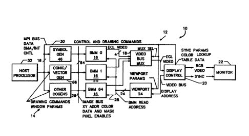
An image processing system 10 with a raster image
generator subsystem 12, shown in FIG. 1, includes
provisions for multiple image cogenerators 14, multiple bit
map memories (BMMs) 16, a video bus multiplexer 18, and a
display controller 20 which governs the display on an RGB
monitor 22. Hardware viewport control is provided by a
viewport controller 24.
The cogenerators 14 communicate with the BMMs 16 via
an image bus 26, while the BMMs communicate with the
display controller 20 via a video bus 28, which includes
the video bus multiplexer 18. A host processor interface
bus 30 provides for communication between the raster image
graphics subsystem 12 and a host processor 32. Examples of
commands and data sent along the host processor interface
bus 30 include drawing commands to the cogenerators 14,
selection signals to the video MUX, viewport priority, size
and location commands to the viewport processor, as well as
commands to the display controller 20. The image
cogenerators 14, a cogenerator bus and memory interface
unit 34 are sub-functions within each generator.
The display controller 20, detailed in FIG. 2,
includes a parallel-to-serial converter 36, a color look-up
table 38, and a digital-to-analog converter (DAC) 40 which
provides the input to drive a red-green-blue (RGB) monitor.
Synchronization among these components and the cogenerators
is coordinated by a
;"
131~7~ 5
synchronization module 42 which generates conventional
IEEE standard RS 343 video synchronization signals in
response to timing signals from a display clock 44.
The host processor interface (HPI) bus 30
provides a path for a graphics or input/output processor
to send drawing commands and data and control messages
to the raster image cogenerators 14. It is a general
purpose bi-directional 16-bit data path. More recent
embodiments use a 32 bit wide host processor interface.
The host processor interface has been configured
to work efficiently with different types of display
drivers by providing direct memory access (DMA)
handshake lines and WAIT and ACK signals. For example,
the host processor interface can drive a display system
on a fir$t-ln-first-out (FIF0) basis. Alternatively, a
fast processor can be used to drive the generator
directly using programmed input/output.
The interface has been configured to be easily
connected to the standard busses such as the Intel
Multibus. This interface supports DMA or programmed
read or write rates of up to 200 ns per 16-bit word,
with an average drawing command reguiring about 3-5
words.
Each raster image generator device occupies at
least two addresses in the processor I/0 space. Command
conventions and word formats were selected to allow
generalized software procedures.
13~71~
The image cogen~erators 14, including those
illustrated, as well as others, are a family of devices
ranging in complexity from a simple gate array device to
several 5x5 cards, each constructed to generate one type
of figure or image. Several basic types are listed
below.
By way of example, three cogenerators are
respectively illustrated in FIGS. 3, 4 and 5. As will
be described in more detail subse~uently, a symbol
cogenerator 46 of FIG. 3 includes a symbol generator
gate array 48, w~th a font bank 50, which responds to
signals from the symbol generator gate array 48 by
outputting to a transform module 54. The font bank 50
provides eight 256 symbol fonts, with unlimited strokes
per symbol. The contents of the font bank may be
downloaded by the processor or may be stored in ROM.
The output of the transform module 53 is a return to the
symbol generator. This arrangement makes font selection
and modification convenient. The transform module
accepts stroke information as an input and produces
scaled and rotated stroke data as output.
The symbol generator gate array 48 is controlled
by the RD/WR line 54 and a bi-directional 16 bit data
path 52 to the controlling processor. The symbol
2S generator gate array 48, in turn, outputs pixel
addresses to the memory interface unit 34 via a local
address bus ~8 using simple WAIT handshake. The address
space corresponds to a 4Kx4K BMM address.
13~3~5
The memory interface unit 34 formats the output
of the symbol cogenerator 46 for input to one or more of
the bit map memories 16 via the direct memory access
image bus 26. This transmission requires handshaking as
indicated on a REQ/~NT line 60. Performance monitoring
and fault localization are provided by the SETSCAN lines
62 and the SIGNATURE lines 64. These functions are
described in greater detail below.
The symbol generator 46, illustrated in FIG. 3,
generates scaled and rotated symbols, alphanumerics and
vectors. It also maintains an internal typewrite cursor
with automatic carriage return for alphanumeric strings.
Eight font sets of 256 symbols or characters each may be
downloaded to RAM or stored in PROM. The cogenerator
contains hardware windowing logic which may be used to
scissor symbols on a pixel by pixel basis to an
arbitrary x,y region or to pick a symbol which falls
within a region. The symbol generator generates pixels
at a 10 MHz rate which translates into an average symbol
drawing time of .005 msec including bus transfers.
Additional features of the illustrated symbol
generator 46 are a typewriter cursor with programmable
line and symbol space, 64 rotate angles with 60 angles
being programmable, 16 scale factors with 12 being
programmable, window clipping or picking, and 100
nsec/pixel calculation rate.
A conic/vector cogenerator 66, illustrated in
FIG. 4, includes a conic/vector generator 68, which has
access to a sin/cos read only memory 70 in determining
23
~3~
addresses for the memory interface unit 34. Commands
and data are sent to both the conic/vector cogenerator
gate array 68 and the memory interface card 34 on the 16
bit data bus 52 and under control of the read/wr
line 54. A local interface bus 58 governs communication
between the conic/vector generator gate array 68 and
the memory interface unit 34, as well as interfacing to
optional anti-aliasing logic 72. The general purpose
configuration of the interface bus and the memory
interface unit allow the anti-aliasing to be enabled or
disabled without any hardware changes. Anti-aliasing
requires that each pixel have a different color value
which requires the memory interface unit to perform a
different kind of memory cycle. This switching is
performed automatically by the hardware if anti-aliasing
is se}ected. As in the other generators, the memory
lnterface unit 34 directs its output to one or more BMM
via the DMA image bus 26, the communication being
regulated by control signals over the REQ/GNT line 60.
The conic/vector cogenerator 66 generates tangent
and dx, dy vectors and vector chains, rectangles,
circles, ellipses and partial arcs. Textures of dot,
dash and user specified patterns are available.
Contains a hardware windowing circuit which may b used
to scissor figures on a pixel by pixel basis to an
arbitrary x,y region or to pick a figure which passes
through a region. It generates vectors at 100
nsec/pixel and conics at speeds ranging from .5 msec to
4 msec per octant depending on size.
24
1~ 3~5
One of the other image generators, which can be
used, for example, in marine applications, is an
acoustic generator 74, as illustrated in FIG. 5.
Sensory data is DMA input to a first-in-first-out (FIF0)
memory 76 and then directed to a pixel formatter 78.
The pixel formatter 78 responds to control signals to
provide for different pixel formats. A conic/vector
cogenerator 66 is included to accommodate circular
formats. A pixel mover 80 with associated RAM 82
provides for high-speed movement of arbitrary rectangles
within the displayed image.
In the acoustic generator 74, a microprogrammed
controller 84 reads 32-bit acoustic data words from bulk
memory, and controls the pixel formatter 78, the pixel
mover, and the conic/vector generator 68 gate arrays to
produce different raster formats and waterfalling. The
pixel formatter 78 is used for raster update; the pixel
mover 80 is used for waterfalling; and the conic/vector
cogenerator 66 is used for point position indicator
formats.
Several other types of image cogenerators 14 have
been defined. These include a radar scan converter,
seed area fill generator, NTSC video grabber and image
processor. Each cogenerator has identical host
processor 16 and image bus 26. The general purpose bus
architecture provides both the performance and
functionality required for real-time sensor imagery. A
radar scan converter cogenerator can be added to convert
azimuth/range format digitized radar video inputs into
1313~
x,y raster format and ~erform aging on the data in
either x,y raster or azimuth order.
An image processor cogenerator can be added to
perform simple image processing by performing
read/modify/write memory cycles and passing the image
data through a dedicated arithmetic logic unit (ALU).
A seed fill cogenerator can be added to seed
fills predefined regions with solid color or patterns.
The estimated performance of this cogenerator is a fill
rate of around 15 million pixels per second. A polygon
fill cogenerator can be added to provide filling of
convex polygons of up to 256 sldes. Fill rates approach
160 million pixels per second for large polygons.
Each cogenerator receives commands and data from
the controlling processor and generates pixel addresses,
color data, and/or pixel enables to produce a raster
image. ~he symbol and conic/vector cogenerators produce
pixels at a rate of 10 million pixels per second for
lines, symbols and alphanumerics.
Since cogenerators run in parallel and may be
duplicated, very high writing rates may be achieved. A
high degree of modularity is also achieved sinca
different types of cogenerators may be added by plugging
in a card.
An image bus provides a versatile, low level
interface standard at the image cogenerator output,
which allows cogenerators to drive image data to the
26
.
13~ ~7~ 5
memory interface unit 34 and to read data bac~ from the
BMM. It consists of 24 pixel/word address lines, 16
pixel enable bits, 12 color bits, 12 color mask bits,
and several control signals. The cogenerator bus allows
up to 16 pixels all the same color falling within a
single BMM word to be transferred in 100 nsec.
Bit map memory write operations require address,
color value, and a pixel mask, for word operations, to
be provided. Since different cogenerators provide these
in different sequences, or in the case of color the
value may come directly from a processor rather than a
cogenerator, separate load outputs corresponding to each
parameter are provided. Each load term is activated
when the corresponding data is available. ~he memory
interface unit begins a memory operation when the load
address LDADD term goes active. It is the
responsibllity of each cogenerator to ensure that all
required parameters have been loaded into the memory
interface unit before issuing LDADD. A simple WAIT
control provides synchronization.
The memory interface unit 34 is a single chip bus
controller for the image bus 26, detailed in FIG. 6.
The memory interface unit provides a path for the host
processor 32 to send commands to and read status from
smart BMMs 16. The command path is generalized for
growth to complex smart BMM designs containing ALUs,
zoom or windowing logic. It allows multiple data
sources (cogenerator/memory interface units) using
request/grant arbitration and up to 64 BMM.
27
The primary function of the memory interface unit
is to provide an efficient, simple means of interfacing
cogenerators to the image bus. In this case, the host
processor initializes the memory interface unit, by
sending commands through a cogenerator, to perform a
particular type of image bus operation such as write
pixel, write word or write command, etc. Once
initialized, the memory interface unit automatically
performs the selected operation each time the load
address control input (~DADD) is activated. It will
request access to the image bus, issue the appropriate
control code, format the address and data words, and
transmit them only to the bus in the correct time slots.
Several pipeline stages within the memory interface unit
assure efficient data transfers.
The memory interface unit 34 also contains a
special pixel buffer to improve the drawing rates of
sequentially addressed figures such as lines, conics and
symbols. The pixel buffer may be configured lxl (x.y),
16xl (x,y) or 4x4 (x,y). Each image cogenerator selects
the organization which provides the maximum number of
pixels per transfer. This would be 4 x 4 for vectors,
conics and stroke drawn symbols, and 16 x 1 for polygons
and dot matrix type symbols. The lxl format is included
to support BMM designs which do not allow full word
operations.
As address inputs are received from a
cogenerator, the pixel enables are collected in the
pixel buffer until the address moves outside the word.
A pair of pixel buffers are used with one being filled
28
13t ~7~ ~
while one is being loaded to minimize overhead. A WAIT
is issued to the cogenerators if the memory interface
unit cannot accept new pixel data.
The image bus consists of a 64-bit multiplexed
data/address/command bus, 7 address lines, 5 bits of
operation control code, clocks and the request/grant
signals from each source. The configuration of the
memory interface unit, the arbiter and re~/grant
handshaking eliminates any wasted bus transfer when
switching between cogenerators.
A single pixel of 1-12 color bits or a single
word of 1-16 pixels (all the same color) may be read or
written in one bus cycle (100 nsec). This allows some
forms of drawing (area fill) to be performed at up to
160 million pixels per second.
A special bus operation is included to allow an
4 x 4 x 4 (x,y,color) or 4 x 2 x 8 pixel block to be
read or written in 1 bus cycle. This is designed to
support high speed textured area fill or sensor (radar,
acoustic) display generation where each pixel may have a
different color value. A simple WAIT control is used to
synchronize transfers. The area fill cogenerator does
not load the pixel buffer one pixel at a time, but 16-
bit parallel at a time. It can therefore use every bus
cycle on the image bus.
A11 operations on the image bus 26 are addressed
either to an individual BMM card, using its physical
address, or to a predefined group of up to 12 8MM planes
29
~ 3 ~ 5
using a transparency identifier. This address value is
sent each bus cycle on the 8 address lines and is
compared on the BMM card to its physical address and to
its programmed transparency identifier.
A wide range of BMM configurations are compatible
with the raster image generator architecture. The
addressable word organization may be lxl, 4x4r 16 x 1,
or 4x2 (x,y), while the physical word organization must
be equivalent or a superset (i.e., 32xl to support
16xl). The BMM address space is 4Kx4K with paging used
to expand beyond that. As a minimum, the BMM support
one of the image bus write operations, the logical and
physical addressing logic and the commands to program
address and color bit posit~on within a transparency
~(bit map memory group), and enable or disable the video
output.
The image bus has a generalized command operation
which may be used to control any special functions on
the BMM such as windowing, test, fill, and video
functions such as pan, zoom, scale, etc. The image bus
also allows readback of status from a BMM plane. If a
8MM plane cannot execute the image bus cycle, it
asynchronously asserts the WAIT signal.
Each BMM outputs digital video data under control
of either the display address or the BMM serial sync
signals on the video bus 28, FIG. 1. The BMM card will
interface to the image bus which has the cogenerator
clock ~at 10 Mhz) and to the video bus which has the
~ 3~ ~3~ ~
video bus clock tat pixel clock rate divided by 4 or 8).
These clocks can be different frequencies.
The video bus 28 is the path for video display
addresses and synchronization to pass from the display
control function to the BMM and for digital video data
to flow back from the BMM to the display controller 20.
In the illustrated embodiment, the video bus MUX 18 and
viewport control functions are imbedded into the video
bus. Herein, functions are "imbedded" when their
existence is transparent to the 3MM and display control
on each end of the bus. These controllers, as well as
alternative imbedded controllers, simply transform the
data or addresses flowing across the bus under
independent control of the host processor.
In the case of the viewport controller 24, the
host processor programs the device with the viewport
parameters such as display position, size, BMM read
address, and transparency BMM groups to be displayed.
The viewport controller then compares the display
address (which it generates internally) to these
parameters. When the display position for a given
viewport is reached, the viewport controller outputs the
BMM read addresses for the viewport in place of the
normal display address it had been passing through. If
more than one viewport occupies the same display
position, the highest priority viewport is used. Each
viewport controller provides a full screen bac~ground
plus 4 prioritized programmable viewports. The devices
may be cascaded to allow up to 20 viewports per display
controller. Each display controller has an independent
31
,
1 3 ~
set of viewports. Each BMM plane contains logic which
compares a software programmable mask value with the
current viewport code sent from the viewport controller.
If the mask has an enable bit in the position
corresponding to the viewport number the BMM output is
enabled. This allows the software to select which
planes (transparencies) are being displayed within each
viewport.
FIG. 6 shows an example of hardware viewport
usage in a tactical disp}ay system. The hardware
viewporting allows an image to be displayed out of one
portion of the BMM while an updated version of the image
is being built in another region. Menus may be stored
in the BMM and enabled for display instantly without
requiring them to be regenerated each time. The display
controller allows a different color palette for up to 8
viewports.
The video bus MUX 18, accepts several BMM outputs
as input and contains multiplexers to connect any input
to any one of the output channels which drive the video
bus data lines. The processor programs a connection
pattern into the video bus MUX logic which causes the
BMM outputs to be switched to the appropriate video bus
channel to implement plane toggllng or dynamic BMM
2S allocation.
Each BMM plane has a 4-bit emitter-coupled logic
(ECL) output driver which, when enabled, supplies four
horizontal pixels of data per video bus clock to a shift
32
7 ~ 5
register on the display controller 20. In a system
requiring toggling memory planes, these outputs may
simply be wire-ORed together and toggling accomplished
by turning the planes on and off by sending commands
across the image bus. If dynamic plane allocation is
required, a MUXing function may be added between the BMM
16 and the display controller 20 which accepts commands
via the host processor interface.
The video bus 28 contains 22 bits of display
address which the BMM may use directly to read the
display data, or the BMM may calculate the display
address by decoding a serial control signal which
provides horizontal and vertical synchronization codes.
The display controller 20 receives 4-bit parallel
d$gital video data from the BMM 16, converts it to
serial, sends it though the color look-up table 38 and
video digital-to-analog converters (DACs) 40 to produce
RGB color or monochrome video outputs, as shown in
FIG. 2. The display control also contains a SYNC gate
array which supplies TV raster sync timing, display
address for BMM reads, serial sync for BMM use, and the
color look-up table download control timing.
The image bus 26 governs the flow of commands,
data and addresses between the memory interface units 34
and the bit map memories 16. As shown in FIG. 7, the
image bus 26 includes an arbiter 88, as well as a system
clock 90.
1~13~5
The image bus .26 consists of 64 bits of
directional data lines, 7 BMM plane select lines and 5
control lines. One of the control lines is a wait
signal for synchronization and the other four signals
indicate the bus cycle. The bus connects up to 8 memory
interface units to up to 64 BMMs. Since the image bus
is a general purpose bus, other sources besides the
memory interface units may reside on the bus to
interface with the BMMs.
The image bus 26 interfaces to BMMs 16, memory
interface units 34, and other sources. The memory
interface units or the other sources have the ability to
become the bus master and control the bus. The BMMs,
however, do not control the bus. A bus master may
perform any of the cycles, described below, available to
the memory interface unit.
The memory interface unit 34, once in control of
the bus, may perform either command or data operations.
For each bus operation, the memory interface unit first
outputs what type of cycle it is to perform indicted by
the bus command (ICMND), and what BMM planes are
selected for the operation indicated b~ the BMM plane
selection signals (IPHYS, IGRSEL, IADR) and on the next
bus cycle perform the actual command or data transfer.
.
If the BMMs determine that they will not be able
to perform the requested operation, they store the ICMND
code and issue a WAIT to the memory interface unit. If
a WAIT occurs, the memory interface unit stops in its
present state until the WAIT is taken away, at the same
34
~3~3~ 5
time is output another I~MND code for the next cycle If
the bus is not going to be used for a cycle the memory
interface unit sends the code for IDLE to the BMMs.
During the time WAIT is active, the ICMND must be set to
IDLE. Another time when the IDLE is required is when
none of the memory interface units are using the image
bus.
THe BMMs 16 all perform the same cycles when
addressed so that they remain synchronized. If for
example, some of the planes are mas~ed out by the color
enable field during a write operation, they still
perform the cycle without modifying their contsnt. This
reguirement also synchronizes the generation of IWAIT by
the BMMs within a transparency. Either all or none of
the planes in a transparency issue IWAIT.
The memory interface units write to BMM all the
color bits of up to 16 pixels during one bus cycle if
all the pixels are the same color, and if the pixels
have different colors, the operation involves performing
additional data cycles. Each data cycle can write up to
4 bits of color information for all 16 pixels. A mixed
mode operation is also possible in which some of the
color bits are the same for all the 16 pixels and some
are different. The same color information will be sent
with the address and the different color information
during the following data cycles.
Reading the color values of one pixel or partial
color bits of up to 16 pixels is possible in two or more
cycles. During the first cycle the address is sent to
1 3 ~ 5
the BMMs 16 and the data is read back during the next
cycles. Reading the coior of one pixel requires only
one data cycle, and reading the color of 16 pixels
requires one data cycle for each group of 4 planes.
The image bus 26 supports two types of command
cycles. One is the "address command" and the other is
the "global command" cycle. Only the BMM planes which
are addressed will respond to the first cycle, but the
second cycle applies to all the planes connected to the
image bus. The command cycles are of generic type, and
the details of the word formats for the different
commands are not defined in this document. The contents
of the OPCODE and the COMMAND fields are determined
based on the type and the capabllities of the BMMs used.
Examples of image bus operations include: read
color of one plxel, FIG. 8a; read color bits of 16
pixels, 12 color bits per pixel, 4 bits in each group,
FIG. 8b; write all color bits of 16 same color pixels,
FIG. 8c; write all color bits of 16 different color
pixels, 12 color bits per pixel, 4 bits in each group,
FIG. 8d; write all color bits of 16 bits pixels with
some color bits the same and some different, 12 color
bits per pixel, 8 bits the same and 4 bits different,
FIG. 8e; read status of a transparency group,
unmaskable, FIG. 8f, send maskable command to all the
BMMS to set some parameters, FIG. 8g.
Th~ bus arbiter 88 per~orms operations such as:
1) accept bus requests; 2) priority select bus masters;
3) issue bus grants; and 4) re-clock the BMM WAIT
1 3 ~
signal. To gain bus access and become the bus master,
each memory interface unit must first issue a bus
request to the central bus arbiter. A bus request will
be issued during a bus cycle. This request is meant for
the next bus cycle. The bus arbiter must select the
next bus master before the end of the cycle.
The selection of possible bus masters can be
based on a priority scheme, when the highest priority
requestor is always granted the bus, or some other
selection method. Different arbiters can be designed
for different system requirements. The illustrated
arbiter has the following characteristics. First, once
the arbiter determines the upcoming bus master, it
issues a synchronous bus grant to the proper requestor.
Second, no cycles are wasted in transferring the control
from one memory interface unit to another. Third,
operations which require more than one bus cycle are not
interrupted by the arbiter until they are finished.
Fourth, the GRANT is held active for the last memory
interface unit in control of the bus until the memory
interface unit has completely finished its operations.,
i.e., the REQUEST is taken away, and the WAIT is not
- active either. Finally, the arbiter re-clocks the IWAIT
signal for the memory interface units.
The image bus signals shown in FIG. 7 have the
following definitions.
IDATA is a 64-bit address and data bus. All the ~MM
word formats will be transferred on this bus.
It is used as a bi-directlonal lnterface
between the bus elements discussed in the
previous section.
ICMND iS a 4-bit parallel code sent from the memory
interface unit to the BMMs. This code is used
to define what the upcoming bus cycle will be.
The description of these codes are defined in
the next section.
ICONFIG is a l-bit code specifying the configuration
of the image bus word formats. The data for
the 16 pixels, during an image bus half word
operation, can be configured either as a 4x4
matrix or a 16xl matrix.
IPHYS is an input signal to the BMMs to specify how
the BMM is to interpret the BMM address. The
address can be either a physical or a
transparency address.
IGRSEL is a 2-bit number selecting the BMMs within a
transparency that are to respond to the next
data cycle if transparency addressing is used
with more than four planes. If physical
addressing is selected, these two bits are a
part of the physical address for the memory
planes.
IADR is a 4-bit transparency address. During the
next bus cycle, only the BMMs that have this
transparency address will respond to the bus
38
13~3~ ~
cycle. However, if physical addressing is
selected, the 2 bits of the IGRSEL are
combined with this address to form a 6-bit
physical address.
5 -IWAIT is an active low output generated by the BMMs
to stop the bus master. This signal should
become active as soon as the BMM determines
that it cannot perform the next cycle. The
bus arbiter u pon detecting this signal
activates the -ISWAIT which ~s the synchronous
version of the IWAIT signals for the memory
interface units. (If IWAIT becomes active
after the bus master has released the bus, the
arbiter should keep the last master on the bus
until the IWAIT is taken away.)
-ISWAIT is the re-clocked version of the IWAIT signal.
-IREQ is an active low output signal from the memory-
interface unit to the arbiter. This signal
becomes active asynchronously when the memory
interface unit decides to use the image bus.
After completing the bus operation the memory
interface unlt releases the bus by tak~ng this
signal away.
-IGRANT is an active low synchronous input signal to
the memory interface unit indicating that the
request to use the image bus is granted and
the memory interface unit may perform its
39
:
1313715
operations. The GRANT becomes inactive after
the request is taken away.
SYSRA is a memory cycle sync signal generated on the
clock card and distributed to all the BMMs.
SYSCLK is the system clock generated on the clock
card and distributed to all the image bus
elements.
The image bus is capable of performing all the
bus cycles that can be specified by the image bus
command code ICMND as indicated ln the following table.
The encoding of the fo~r bits of the ICMND is shown in
FIGS. 8a-g. The ICMND word format is shown in FIG. 9a.
R/W A/D/C/G AUX CYcle
15 0 00 0 Write Address Same Different Color
O 00 1 Write Address Different Color Only
O 01 0 Write Data
O 01 1 Write Data
O 10 0 Write Unmaskable Command
20 0 10 1 Write Maskable Command
O 11 0 Write Unmaskable Global Command
O ll l Write Maskable Global Command
1 00 0 Read Address Pixel
1 00 1 Read Address Half Word
25 1 01 0 Read Data
1 01 1 Read Data
1 10 0 Read Unmaskable Command
1 10 1 Read Maskable Command
1313715
1 11 0 Read Unmaskable Global Command
1 11 1 Read Idle
R/W--Read/Write
0 = write
1 = read
A/D/C/G--Address/Data/addressed Command/Global Command
00 = Address
01 = Data
10 = Command
11 = Global Command
AUX--Auxiliary bit
Read, Address:
. 0 = 1 pixel
1 = 16 pixels
i5 Write, Address:
0 = same and different colors
1 = different colors only
Command:
0 = Unmaskable
1 = Maskable
Global Commands:
0 = Unmaskable
1 = Idle-
Each read operation requires at least two bus
cycles. During the first cycle the address is sent to
. 41
the BMM, and the data is~received during the next cycle.Some write operations can be per~ormed in one cycle and
some may requires more than one cycle. The BMMs are
always able to perform data cycles after each address
cycle. The data cycles, however, do not have to follow
the address cycle during write operations. The same
color information is included during the address cycle
and the different color ones are sent during the data
cycles. The same color information may or may not be
enabled by the AUX bit in the ICMND code.
The 12 color enable bits allow selective masking
of the color planes. Each bit set to 1 disables
different color write operation to the corresponding
plane and enable same color writes to the same plane.
The different color operations may take up to four bus
cycles to complete.
Each enabled plane is disabled for different
color writes, and each disabled one is enabled for
different color writes. These bits can also be used as
extended color bits if more color bits are reguired by a
system.
Although this cycle is called "Address cyele",
for some operations, it contains more information than
just the address. It includes chip enables (one bit for
each pixel), same color data (12 bits), and color enable
bits (one bit for eaeh bit plane~. For operations whieh
do not require these parameters, these fields are
ignored by the BMMs.
42
.
13~3~1~
Three major word formats are address, data and
command; each cycle type has its own formats. The
address cycle word format is illustrated in FIG. 9b.
The data cycle word format for color data of one pixel
read from memory is shown in FIG. 9c, while the data
cycle word format for partial color data for 16 pixels
during write or read is shown in FIG. 10a. The word
format for a command cycle is shown in FIG. 10b. The
timing for the image bus ADDRESS cycle and the WRITE
DATA cycle is shown in FIG. lla. The timing for the
image bus READ DATA cycle is shown in FIG. llb.
X ADDRESS
Pixel address if pixel memory is used.
Half word address if half word memory is used.
Y ADDRESS
Pixel address if pixel memory is used.
Half word address if half word memory is used.
CHIP ENABLES
Write enable bits for half word writes.
Ignored if pixel memory is used.
COLOR
Color bits for 1 pixel if memory used.
Color bits for 16 same color pixels.
COLOR ENABLES
Write enable bits for color planes.
43
13137~5
At each positiqn
O = disable corresponding color bit.
1 = enable corresponding color bit.
All commands should be sent during this command
cycle. An IWAIT may be issued during a maskable command
cycle. The reason for the command cycle distinction
between maskable and unmaskable is to allow the BMM to
issue waits when commands will interfere with the BMMs
performance. An example might be changing the size of a
window when the BMM is in the middle of a window
operation.
If a command is part of the unmaskable group,
then it is sent during the unmaskable command cycle.
The IWAIT is not issued to an unmaskable command.
The IPHYS, IGRSEL and IADR word formats, the
timings for which are shown in FIG. llc, are as follows.
IPHYS Physical/Transparency
O = Physical
1 = Transparency
~0 IADR Memory select address
Transparency address or
4 LSBs of physical address.
13~3~
IGRSEL Group Select
For Transparency addressing:
00 = planes 0-3
01 - planes 4-7
10 = planes 8-11
Acoustic Displav Svstem
In accordance with a preferred embodiment of the
present invention, an acoustic console 201, illustrated
in FIG. 12 includes two high resolution monitors 203,
which are preferably color RGB monitors, although, one
or both can be monochrome. The acoustic console 201
includes a contrsl panel 205 with a keyboard 207 and
trackba}l 209. Beneath the control panel 205 and
monitors 203 is a televislon acoustic generator drawer
lS 213 for current electronics and an expansion drawer 215
to permit extension to new applications and
incorporation of advancing technologies.
The television acoustic generator 217 of the
acoustic console 201 are illustrated in FlG. 13. An
input/output port (IOP) 219, manages communications with
an external computer. Since high speed is a priority
i for the lOP 219, the present embodiment utilizes a fast
bit-slice processor. The IOP 219 interfaces with a
panel processor 221 which provides for interfacing with
standard commercial busses along an RS-422 bus.
An applications processor 223 and a system PROM
and support module 225 interface with the IOP 219 and
.
13~7~
the panel processor via the host processor lnterface bus
227, as well as to bulk memory 229, an acoustic
processor 231, and a graphics processor 233, also
referred to as local host processors. The bulk memory
229 is connected via a direct memory access (DMA)
controller 235 to the applications processor 223, and
two cogenerators, an acoustic display generator 237 and
a pixel mover 239.
The graphics processor 233 controls a conic
generator 241 and a symbol generator 243. The image
generators of the acoustic and graphics channels draw
into bit map memories 245. The contents of the bit map
memories are used as raster output by display
controllers 257 to drive the acoustic console
monitors 203.
Some of the incorporated features of the
illustrated acoustic console 201 include high
resolutions television display of 1280 by 1024 pixels
with functional emulation of the standard OJ-452
displays. Support is provided for a 256 symbol font,
programmable symbols, conics, vectors, rasters,
amplitude scans, point position indication (PPI),
waterfall updates, and format or line orientation.
Increased performance, functional flexibility and growth
capability are provided with respect to graphics in area
fill, rotation of symbols, increased data load and
color. Likewise, enhanced acoustic application is
supported by PPI line orientation, elimination of PPI
stern blinking, increased data load and color.
46
1 3 ~ 5
The incorporating acoustic console 201 is
designed to meet the hi~h performance display
requirements of the next generation of acoustic sonar
systems while also accommodating existing systems. The
design is based on current LSI CGA technology which
enables the design to be more flexible, modular, compact
and reliable as well as less expensive.
Because the acoustic console 201 is designed be
used for many types of applications, such as surface
navy and submarine environments, it is designed with
special features so as to be adaptable to these diverse
requirements. Some features are included to anticipate
the future growth requirements- and are not currently
used. New systems which utilize all the new features of
the unit will gain improved performance, due to the
efficiencies they add.
Such features as compatibility with high level
image definition languages, as well as compatibility
with primitive languages, which essentially controlled
hardware directly, have been included. The ability to
draw images with more than 4 bits pér pixel also meets
requirements for color images with up to 12 bits per
pixel. Larger resolution screens can be accommodated to
provide for expansion to a full 4096 x 4096 pixel
screen.
The functions of the acoustic display generator
237 are all programmable, modular devices which can
easily interface to a standard bus. This allows them to
be used in a host of diverse applications and system
47
131~5
architectures. The performance meets or exceed mo~t
currently used acoustic consoles in build and update
times. One of the major features of the design is its
compact modular architecture, which is based on
functional modules, called cogenerators which are highly
specialized and high performance units dedicated to a
category of drawing type. If unforeseen new functions
are needed in the future these can also be added to the
bus.
Depending on the types of drawing required in the
system there are special purpose functions which enable
fast image generation. Such functions allow efficient
and fast drawing of characters of various size and
orientation, conic sections for drawing vectors, curves,
circles and ellipses, acoustic raster data unpacking,
stretching, compression, and pixel field expansion.
Other functions allow manipulating the existing image in
bit map memory at a high rate in such ways as area
translation, area rotation, combining or inverting
images and area fills.
Some of the main features of the advanced
acoustic display generator are the following. All of
the cards fit within a single drawer 213 of the
acoustic console 201. The monitors 203 are driven with
single pixel resolution; monochrome resolution is 4
bits/pixel and color resolution is 8 bits/pixel. Normal
and reduced gain emulation are provided, as are blink
and reverse video modes.
48
1 3 ~
The build rates .are 200 ns/pixel for unpacked
data and 50 ns/pixel for packed data. Waterfalling of
rasters is between 25 ns/pixel and 40 ns/pixel. Other
performance parameters include: circle PPI generation
is less than 10 ms with controller or 200 ns*8*radius
with the conic/vector cogenerator, vectors can be drawn
at the rate of 200 ns*pixel length. The DMA interface
allows data to be accessed at 300 ns per 32-bit word.
The symbol draw rate is approximately equal to the
number of on pixels in the font times lOO ns.
All the build, waterfall and vector draw rates
include only the build rates with the hardware and not
the interpretation and set of times using the controller
and control host processor process times are only
roughly estimated. It should be added that digital
technology is employed to reduce costs and enhance
reliability. The modular constructions allows for
future growth.
The currently planned uses of the acoustic
cogenerator and RIG devices include such diverse
acoustic terminals for the surface Navy and the
submarine environments. The capability of some of these
functions are not tied only to SONAR applications and
are applicable to such diverse uses as radar, trainers,
simulators, and tactical displays.
The graphics processor 233, the acoustic
processor 231 and the panel processor 221 can read
command or data from the bulk memory 229, interpret
those commands and command the implementation of the
49
13~7~5
commands to be executed by the acoustic display
generator 237, one of the graphics generators 243, 241,
249, etc., a standard bus panel via the panel processor
221, or performance monitoring and fault analysis
modules 263 or any special hardware function through
their local host processor interface (HPI).
The acoustic console 201 uses several separate
control processors. One for the "acoustic channel"
control, one for the "graphic channel" control, and one
for the panel interfaces was envisioned for a typical
acoustic console. If such parallelism is not necessary
then these channels can be combined and controlled by a
common high performance processor.
The graphics channel, defined by the graphics
processor 233, is a dedicated set of cogenerators, and
bit map memories whlch are used to bulld and store
graphic images independent of the acoustic processors
and cogenerators. Graphic lmages functions include
display of text, symbols, and cursors which can also be
blinded. The graphic bit map memories are separate from
the acoustic bit map memories so that a change in any
text, symbol or cursor does not cause any of the
acoustia data to be destroyed in the bit map memories.
; The graphics channel is controlled by the
graphics processor 233 which lnterprets all command
messages in the bulk memory and generates control
messages to the symbol or conic cogenerators. It also
supplies the data to the cogenerators after reading data
SO
13~3~
from the bulk memory 229 and reformatting it in
accordance with the cogenerator reguirements.
The firmware which is responsible for controlling
the graphic cogenerators is called a virtual raster
image generator subsystem driver. This standard
interface program is used to format messages and data
for the graphics cogenerators, bit map memories, and
keep system parameter and status data required to
manipulate the hardware.
The acoustic console 201 includes the acoustic
channel 265, which is shown ln isolation in FIG. 14.
The acoustic channel 265 includes the acoustic
processor 231, and the acoustic display generator 237
coupled to bulk memory 229. The acoustic channel 265
also shares some of the bit map memories 245 and the
display controllers 247.
The acoustic channsl 265 generates, updates and
stores acoustic images that are displayed on the
monitors 203. The acoustic channel uses its bit map
memories 245 for storing acoustic data primarily. The
acoustic processor 231 controls the acoustic channel
from control and data files in bulk memory 229 which it
can read and interpret.
~he acoustic display generator 237 is detailed in
FIG. 15 and includes an acoustic controller 267, which
responds to the acoustic processor 231, and controls the
pixel formatter 269 and, optionally, a conics generator
241. Output is to the bit map memories 245 through the
13~71~
memory interface unit,255. The acoustic display
generator also uses a pixel mover 239 and assoeiated
llne buffers 271 as deseribed below.
The acoustic display generator 237 is a
collection of speeial processors that ean efficiently
build and update acoustic data into bit map memory. The
proeessors are speeialized in manipulating aeoustie data
bases, and building aeoustie formats which differ from
graphies formats. There is a special need for high
speed build and update eapability sinee aeoustie formats
use a very large and dense image formats that require
the manipulation of a million pixels in less than 50 ms
time.
For unpaeking data fields from bulk memory 229
and formatting it properly repacked into pixel data
paekets and repeated the seleeted numbèr of times, the
formatter 269 is used with the aeoustic controller 267.
These two funetions eooperate to generate data and
address coordinates for horizontal or vertieal rasters.
The acoustic display generator 237 is also used to build
ASCANS and PPI formats using the eonic cogenerator 241
or the acoustic controller with a eirele build
algorithm. The pixel mover 239 funetions mainly to
manipulate the image already in the bit map memory 24S.
The aeoustie eontroller 267 is also used as the high
speed algorithm proeessor and eontrol unit to set up,
initialize the eogenerators and to interpret all
messages from speed 16k by 16-bit memory whieh is
aeeessible to the aeoustie eontroller and the aeoustie
proeessor.
52
7 ~ ~
The acoustic processor 231 is a microcomputer
which serves as the main interpreter of control messages
from the external computer. It also formats the control
and data into a standard message format for the acoustic
display generator 237. The hardware driver program of
the acoustic processor 231 generates command files to
the local memory 273 based on interpreted commands from
the bulk memory 229, which are then used by the acoustic
controller 267 to set up and control the other
cogenerators in the acoustic display generator 237.
A dedicated memory for the acoustic processor 231
stores downloaded control programs from bulk memory,
interpreter and hardware driver programs, and test
programs; this dedicated memory also stores statistics
on current display parameters and a directory of the
local memory 273 which it services.
Each processor 221, 231, 233 has its own
independent host proceYsor interface which enables
concurrent operations on the host processor interface
busses 227. These HPI busses serve to isolate local
data exchanges from the system command and data type
traffic of the system bus.
The local memory 273 is a high speed 16k by 16
bit scratchpad memory used to send commands and
formatted data to the acoustic controller 267. It is
used by the acoustic controller as a command buffer to
the acoustic display generator 237 as well as a control
parameter file.
53
131~715
The acoustic controller 267 can read the device
in a random access way and read an initialized DMA port
sequentially. The DMA port access is a s~ngle cycle
read whereas the random access requires a first bus
grant from the acoustic processor 231 followed by an
address cycle then the read or write cycle. The local
memory 273 does not have a separate address port so the
address must be loaded through a common port with the
data.
Besides command messages the local memory 273
also contains display parameters and control tables for
rasters that utilize raster line descriptor (RLD) tables
wh~ch are accessed along with the data in the bulk
memory 229 in a DMA mode. The RLD table defines the
repetition of the input pixels and their locatlon
relative to the start of the line. The index tables
define the manipulation of the data block to cause
orientation of the lines.
The use of the local memory 273 can be made to
fit various system requirements and needs such as a fast
access table for circle generation parameters. This
local memory 273 also includes a fast access table for
circle generation parameters. The local memory also
includes a fast access DMA read port which is accessible
in a single cycle by the acoustic controller 267.
The bulk memory 229 is accessible in two ways.
One way to access it is through its primary 16-bit data
port 275 connected to the system bus 277, which port ls
54
13~71~
accessible to devices o~ the system bus, such as the
acoustic and graphic processors, and the system
input/output port 219.
The other port to the bulk memory 229 is the DMA
port 279 which is controlled by a DMA controller 235
that supplies 32-bit data words to the formatter 269.
The acoustic controller 267, however, can also access
data from the bulk memory 229 by using the formatter 269
as its interface device.
The DMA controller 235 is set up by the acoustic
controller 267 or the acoustic processor 231 on the HPI
bus 227; once initialized, the acoustic controller
handshake signals can reguest data from the bulk memory
229 into one of the line buffers 271 of the formatter
269.
The formatted pixel data from the acoustic
display generator 237, or one of the graphics
generators, is loaded into bit map memory 245 through
the memory interface unit 255. This arrangement
simplifies the image bus interface for the cogenerators
because it generates all the bus commands, bus cycle
timing, and contains address, pixel, and color mask
registers.
The bit map memories 245 have several modes of
operation which enables multiple interfaces to utilize
the image bus 253 without degradation of throughput.
Each memory interface unit 255 allows multiple pixels to
be transferred as well as slngle pixels. The following
7 ~ ~
modes are currently used by the acoustic display
generator 237: 1) single pixel load into a 4 x 4 (4bit)
matrix; 2) 4 x 4 pixel array of 4 bits/pixel with a
single or different color; 3) 4 x 2 pixel array of 8
bits/pixel with a single or different color; and 4)
8 x 1 pixel array of 8 bits/pixel with a single or
different color.
These memory interface units 255 also enable a
simpler bit map memory design because of their ability
to access and manipulate rows and columns of the image
bus matrix data. By being able to collect input pixels
until the boundaries of the matrix are exceeded and then
transferring the matrix, the traffic on the image bus
253 is reduced allowing other cogenerators to use the
image bus in a time-shared mode.
The image bus 253 is a 64-bit wide bus that
allows 16 x 4 bit/pixel data to be transferred or 4 x 2
8-bit/pixel data to be transferred in 2 bus cycles, with
a mask matrix which selects wh$ch pixels in the matrix
are to be modified in bit map memory, and a color mask
which selects which set of bit planes are to be enabled
for update, and the 12-bit X and Y coordinates of the
pixel data. A command çycle, on the separate command
lines, always precedes the transfer of pixel data, mask,
and address on the 64-bit image bus.
The display controllers 257 read the values of
the bit map memories 245 to generate intensity and color
information to the monitors 203 which are output on the
RS-343 interface to the monitors 203. The display
56
131371 5
controllers are programmable to permit various types of
bit map memories to be used with a range of monitors
with different timing, and resolution requirements.
The display controllers 257 read the bit map
memories by supplying the address and control
synchronization to the memoxies in synchronization with
the monitors' raster sweeps and synchronization signals.
The display controllers 257 also convert the pixel
values from the bit map memories 245 into RGB and
intensity by using their color look-up tables. The
color look-up table is downloadable from the host
processor 231 or 233, through the host processor
interfaces of the display controllers 257. A separate
display controller is reguired for each monitor since
the input data to each monitor i8 dlfferent.
Several types of bit map memory architectures can
be constructed using the raster image generator
subsystem BMM modules. The illustrated bit map memories
245 are constructed as 2k by 2k l-bit memories that can
be combined into 12-bit per pixel transparencies.
These can be configured with special features with the
use of a viewport controller or without.
The viewport function allows the translation of
any two dimensional viewport in bit map memory to be
displayed on any location on the visual screen. These
windows can also be set according to priority such that
any overlapping will cause a csrtain priority to be
observed and the highest priority window will be seen.
131371~
Updating a display screen with a currently
displayed bit map memory can cause distortion of the
view screen as new data is added to the old since part
of the screen reflects old data and part reflects new
S data. Ping-ponging, or the synchronous swapping of the
updated bit map memory with the old screen during
vertical retrace, prevents any mixed old/new data to be
ever seen on the screen.
The ping-ponging of the new bit map memories
lC however can be implemented in several ways besides the
old ping-ponging of the whole plane. Because the bit
map memories can be made extra large often the plane can
hold two viewed screen's worth of data and these halves
then can be swapped on and off the visible screen. In
building images to these memories the X and Y addresses
must be offset to ensure that the data is being written
into the proper portion of the bit mapped memory. The
output of these sections can be treated as simple
oversized windows.
Once sufficient windows can be managed by the
viewport function, the various subcomponents of the
formats can be assigned individual windows allowing
acoustic and graphics to be in a common bit map memory
without causing rebuilding of the image when any one ~f
these portions change. The overlapping windows need
only be updated in such cases which doesn't effect the
data in the other windows.
The acoustic console has two monitors 203 which
are both updated and controlled with a common set of
58
13~3~
acoustic/graphics cogenerators. The images for the two
monitors are contained in separate bit map memories and
displayed using separate display controllers 257. Color
or monochrome monitors can be used with the common
acoustic display generator hardware modules.
The impact of color on the acoustic display
generator is minimized by including in the design a 4-
or 8-pixel mode. The impact of these modes is a slower
build and update rate due to the reduced pixel bandwidth
of the busses and processors, causing a 50% reduction in
build and move rates. The corrective action, if the 25
same performance is mandatory, is to duplicate the
memory interface unit 255, pixel mover 239 and formatter
269 although usually all these are not necessary if
there is already a timing margin.
The main interfaces of the acoustic console 201
are the system bus 277, the host processor interface bus
227, the image bus 253 and the video bus 259, as
illustrated in FIG. 16. The system bus 277 extends from
the acoustic console input/output port 219 to the
acoustic processor 231, which controls the acoustic
display generator 231, and the graphics processor 233,
which controls the graphics generators, shown in FIG~ 16
as a generalized graphics generator 281. The generators
interface with the bit map memories 245 and the display
controllers 257 as described above.
Besides the main busses, there are other more
localized interfaces which connect and synchronize a set
59
,
.
1~313'~' ~ rj
of closely related cards. Some of the buses shown in
the interface diagram are multiple since the console
architecture can be separated into separate channels for
higher performance. In s~ch cases, the acoustic and
graphics channel have their own host processor
interface, image and video bus.
The system bus 277 is the major interface of the
acoustic console 201 which is used as a channel to
communicate to the control processors of the unit and
the system memory, which contains all the unformatted
data and control messages that the external host
computer has sent to the unit. Various system bus types
can be accommodated according to the type of n standard"
processors used. The system bus 277 supports a multi-
processor environment which is found on current consoledesigns. Other applications using the Mot~rola 68000
microprocessors use alternate interfaces.
The host processor interface bus 227 is the
second major control interface that interfaces to the
control processors, that are defined as the local host
processors. This interface is used to initialize, and
set up the hardware cogenerators which build the image
from control and data stored in bulk memory 229. In the
illustrated acoustic console 201, the acoustic and the
graphics channels each have their own processors, with
their separate interfaces and bit map memories, so that
they can operate independently of each other for higher
build and update rates.
The host processor interface bus 227 connects a
processor, e.g. the acoustic processor 231, with an
associated raster image graphics device, e.g. the
acoustic display generator 2-~7, using a buffer 283 and a
decoder 285 in con~unction with the multiple signal
lines, as shown in FIG. 17. The host processor
interface bus 227 interconnects nearly all the raster
image graphics subsystem and acoustic generator
functions to the local host processor which serves as a
control processor as it performs all the initialization
and commands to the functions.
The host processor interface bus 227 is a 16-bit
I/O bus which has'the reguired handshake interfaces as
well as programmable interrupt modes for the
cogenerators to operate independently of one another.
Devices can also be programmed to operate in a DMA
transfer mode under the control of an external DMA
controller. Data transfers of 200 ns can be performed
in the DMA mode.
The host processor interface bus 227 is also used
to initialize and perf'ormance monitor and fault
localization sequences. The initialization of some
devices such as the controller's microprogram, the
display controller's timing and color loo~-up table are
performed as well as the initialization of the power-on
reset ~POR) at the beginning of operation. Afterwards,
during operation, the host processor interface bus 227
serves as the main command path to either give commands
directly to the cogenerators, as is done in the graphics
61
131~71~
c:hannel, or to the local memory 273 which is used as the
command buffer in the acoustic channel.
If tests are performed, the host processor can
access the various functions on this bus to command them
to perform a test sequence. The acoustic channel's host
processor interface bus is controlled by either the
acoustic processor 231 or the acoustic controller 267.
When the acoustic controller 267 needs access to
the host processor interface bus 227, it must request
access to it from the acoustic processor 231. Once
given access it can monitor the host processor interface
bus 227 for the time reguired to complete its control
sequence which uses the host processor interface bus.
Normally the host processor interface bus 227 is
released after each short seguence.
The devices of the acoustic channel which access
the host processor interface bus are the acoustic
processor 231, the local memory 273, the acoustic
controller 267, the dedicated memory of the acoustic
controller, the formatter 269, the pixel mover 239, the
display controller 247, and the memory interface unit.
The graphics channel devices which access the local host
processor interface bus are the graphics processor, the
symbol cogenerator 243 and associated memory interface
unit 255, the symbol cogenerator 243 and the associated
memory interface unit 255, the conic cogenerator 241 and
its associated memory interface unit 255, and the area
fill cogenerator 249. The instructions for the host
processor interface bus are given as follows.
62
13~3~ ~
A0 is the address bit 0 is used by some raster
image graphics subsystem chips as the
extension of the normal 16 bits of data.
ACK/ is the acknowledgement of the receipt of a
READ or WRITE request to the device selected
by the requesting device having sent a CS/.
BUSACK/ is an acknowledge from the processor that it
granted the controller's BUSREQ. This is
unused by all other functions.
10 CS/ is a decoded address of the device which
indicates that the current bus master such as
the controller or the processor requests a
read or write to the function.
D0-D15 is a 16-bit bi-directional interface which is
used to send data and commands to each
function on the bus, when they are selected by
the address.
DMARED/ indicates that the function which has been
programmed to do a DMA operation ls requestlng
the next command/data word from the bus
master.
DMAAC~/ indicates that the bus master has released the
host processor interface bus so that the DMA
transfer can be executed.
63
-
,:
~3~7~
INTACX/ iS an acknowledge from the bus master to the
cogenerator indicating that the INTREQ/ signal
has been received and accepted.
INTREQ/ is an interrupt request indicating that the
cogenerator has completed its commanded
operation. This signal is enabled by a
special command or command enable bit and is
otherwise unused and inactive. An interrupt
interface is also required if this is used.
10 POR/ means power-on reset and is a master reset
generated by the power monitor and can also be
generated by the processor. It forces the
devices which have a common POR to initialize
their controls and registers into a
predetermined state.
RD/ is a read select indicating that the bus
master is requesting a write to a selected
function, which is addressed.
WR/ iS a write select indicating that the bus
master is requesting a write to a selected
~unction, which is addressed.
WAIT/ indicates to the bus master that the selected
device can not complete the read or write
operation to the host processor interface bus
as long as the WAIT signal remains low.
64
13~ 3~
ADDRESS selects which functions the bus master desires
to access. The number of addresses used on
any system of course is variable depending on
the number of devices used. Five bits of
address lines is quite adeguate for most
configurations.
The following are host processor interface tHPI)
bus interface addresses used in the illustrated
embodiment. The format of the microprogram memory
address are 15 bits with an additional parity bit.
OOOOX "Host n processor interface
00010 controller
00011 controller initialize and enable
00100 formatter to MIU HPI interface
00101 formatter HPI interface
00110 pixel mover HPI interface
00111 DMA controller
OlOOX conic cogenerator
OlOlX symbol cogenerator
0110X display controller 247 (1)
OlllX display controller 247 (2)
10000 microprogram memory input LSW
10001 microprogram memory lnput MMW
10010 microprogram memory input MSW
10011 spare
lOlOX viewport interface
lOllX spare
11000 local memory data R/W & Increment HPI aAddr.
11001 local memory HPI Address Setup
11010 local memory DMA Address Setup
13l6~
110}1 Spare
11lXX Spare
Timings for the host processor interface bus 227
are shown in FIGS. 18a, 18b and 19, which illustrate the
asynchronous write timing for the host processor
interface bus, the synchronous write timing for the host
processor interface bus, and the host processor
interface bus read timing, respectively.
The cogenerators interface to the bit map
memories 245 through memory interface units 255 which
are used to store all the pixel values, addresses and
control modes required to update or read various sets of
bit map memories. A memory interface unit can receive
single pixel, or pixel rows or columns, or 16 pixe~s
simultaneously and collect these values until its local
4 pixel x 4 pixel matrix boundary is exceeded and then
it outputs to a preselected set of bit map memories 245
on the image bus 253.
Various cogenerators can have their own memory
interface unit, or a single memory interface unit can be
shared. In the case of multiple memory interface units,
a bus arbiter prevents bus contention on the image bus.
Multiple memory interface units enable multiple
cogenerators to be operating at the same time.
The image bus 253 consists of 64 bits of bi-
directional data lines, 7 BMM plane select lines, and 6
control lines. One of the control lines, one is a Wait
66
.
signal for synchronizati.on and the other five signals
indicate the bus cycle type. The image bus connects
multiple memory interface units (up to 8) to up to 64
bit map memorles.
Since the image bus 253 is a general purpose bus,
other sources besides the memory interface units can
reside on the bus to interface with the bit map
memories. The minimum bus cycle time is 100 nsec. The
64-bit data bus is time shared to lnclude 64 bits of
pixel data, 12 bits of X and 12 bits of Y address, 12
bits of color enables, and 16 bits of pixel "chip
enables" to the bit map memories. Separate lines of six
address bits organized in IADR (4), IG~SEL (2), and
IPHYS(l) determine which individual plane or group of
BMM planes is addressed for read or write commands.
The image bus field is formatted as shown in
FIG. 20 with the fields defined as follows:
IPHYS selects the physical address planes when it is
equal to 0 or the transparency addresses when
it is equal to 1.
IGRSEL is the group select line which is used when
the transparency is addressed and IPHYSSl. In
that case 00-planes 0-3, 01-planes 4-7,
10=planes 8-11. However, when IPHYS=0 then
the IGRSEL is simply the MSW of the physical
address while the IADR is the LSW.
67
i3~,3r~ ~ ~
IADR is the address of the transparency when
IPHYS=l or the least significant part of the
physical address when IP~YS=O.
The physical address defines an address for every
bit plane which is unchanged and is determined by which
the planes can be addressed when they are programmed
during initialization. The transparency address
assignments are initialized by using the physical
address.
The transparency address defines a group of
planes which can be loaded as a set with pixel data,
each plane containing one of the bits of the pixel. A
transparency address can contain up to 12 bit planes
which may be loaded in groups. The acoustic
transparency can have 4 bits per pixel, up to 16 pixels
at a time, or up to 8 bits per pixel, 8 bits at a time,
in the matrix. The matrix mode allows faster reads and
writes to bit map memory. In the acoustic channel
normally 4 bits or 8 bits per pixel are loaded into
transparency addresses in the 4 by 4 or 4 by 2 matrix
modes. Single pixel mode is not normally used in the
acoustic channel.
The address cycle includes 64 bits, formatted as
shown in FIG. 21, with the fields defined as fol}ows.
5 COLOR ENA is used to enable each of the 12 possible bit
planes which contains each pixel. A O=disable
of the color bit write while a 1=enable the
color write.
68
13~
COLOR is used when a single color write is
performed, in which case the 12-bit field can
define the color code of up to 12 bits per
pixel .
5 CHIP ENA is used to enable the pixel writes of the
4 x 4 pixel matrix. If the corresponding
pixel enable bit for one of the 16 pixels is
zero then that pixel will not be written into
the bit map memory during a write cycle. One
bit allows each pixel to be written to BMM.
Y ADDR of the control word addressees the Y
coordinates of the bit map memory. It is used
to address the single pixel if the single
pixel mode i8 used or the half work address if
the matrix is used.
X ADDR of the control word addresses the X
coordinates of the bit map memory. It is used
to address the single pixel if the single
pixel mode is used or the half word address if
the matrix is used.
The data cycle includes two forms: the single
pixel mode, illustrated in FIG. 22; and the multiple
pixel mode, illustrated in FIG. 23. The color bit x/y/z
refers to the three possible color planes that each of
25 the four fields writes to.
69
131~1 5
The command cycl~ includes 4 bits of OP CODE,
which is used to initialize the bit map memory mode,
followed by 60 bits of command as illustrated in
FIG. 24.
The arbiter and wait path 283 for the image bus
253 are shown in FIG. 25. The arbiter section inc}udes
an encoder 285, an LE register 287, a feedback loop with
a multiplexer 289, and a decoder 291 which outputs an
IGRANT signal when appropriate. On the memory interface
unit side are a control module 293, a mask module 295, a
clear module 297, an X,Y address module 299, and a pixel
buffer 301, which output to an MIU register 303. The
control module 293 governs the activities of the inputs
to the MIU register 303.
On the bit map memory side of the image bus 253,
a busy signal from a memory control module 305 can be
NANDed with the logic sum of a translated address and a
physical address to generate a -WAIT signal input to a
flip-flop 307 in the arbiter section. Otherwise, data
is output from the MIU register 303 in the memory
interface unit.
The timing for the image bus cogenerator
switching arbitration is depicted in FIG. 26, and the
image bus write timing is shown in FIG. 27. The image
bus address word format, as illustrated in FIG. 28,
includes 1 bit of color enable, 11 bits of color, 12
bits of pixel enable, and 12 bits each of Y and X
address. The image bus cycle types are listed in
Table I.
` 7 ~ ~
TABLE I: IMAGE BUS CYCLE TYPES
R/W A/D/C/G AUX CYCLE TYPE _ _
0 00 0 Write Address Same Different color
0 00 1 Write Address D~fferent color Only
5 0 01 0 Write Data
0 01 1 Write Data
0 10 0 Write Unmaskable command
0 10 1 Write Maskable command
0 11 0 Write Unmaskable global command
10 0 11 1 Write Maskable global command
1 00 0 Read Address Pixel
1 00 1 Read Address Half Word
1 01 0 Read Data
1 01 1 Read Data
15 1 10 0 Read Unmaskable command
1 10 1 Read Maskable command
1 11 0 Read Unmaskable global command
- 1 11 1 Idle
These control lines define the type of operation the
image bus is performing.
The video bus 259, detailed in FIG. 29 is the
interface which connects the bit map memories 245 to the
display controllers 257. The interface is a high speed
emitter-coupled logic (ECL) serial interface, which
takes 4 bits of serial data from each BMM that is
enabled to drive the bus.
71
13~37~
The video bus ~59 includes the video bus
multiplexer 261 with flip-flops 309 to latch incoming
raster data, which can then be selected by the
multiplexer 261 for transmission to the display
controller 257. The video bus 259 also includes a
viewport controller 311, which includes an address
generator 313 which responds to the host processor
interface bus 227 and synchronization signals from the
synchronizer of the current display controller 247. The
address generator 313 transmits the addresses to the
viewport controller 311 which then sends the appropriate
control signals through a bank of flip-flops 315 to a
memory cycle controller 317 and an X,Y storage flip-flop
bank 319 of one of the active bit map memories 245.
A multiplexer 321, ln response to signals form
the memory cycle controller 317, can select the shifted
address so that the appropriate raster data is output
from the bit map memory RAM 323, for output through the
conventional registers 325 and 329 and multiplexer 327.
From there, the raster data proceeds through the video
bus multiplexer 261 and through the shift register 331
of the display controller 247.
The video bus 259 reads out 4 pixels out of each
bit map memory, which are synchronized by the display
controller to update addresses, vertical and horizontal
sync, and pixel clock. The display controller has up to
12 input bits to its table that contains the color and
intensity values. These bit map memories actually
supply the addresses to the tab}e which then supplies
the actual value of the displayed pixels intensity and
72
color. The display cont~oller then converts the values
into an analog intensity and color value, by way of its
digital-to-analog converter, which can produce an RGB or
monochrome signal to the monitors 203.
The video bus timing for the horizontal state
information is given in FIG. 30 (back porch) and in
FIG. 31 (front porch), with the fields given the
following definitions.
-BLANK shows when the video is active on a horizontal
line. This signal may be used to blank out
the output of the video DACs (digital to
analog converters). When this signal is high,
the video should be blanked out. When it is
low, the video is active.
VADDR0-VADDRll are twelve bits of address provided by
the synchronization CGA 333 to show the present line
position of the raster display. These twelve bits can
be tri-stated depending on the /DSADEN input. This
counter is reset at the beginning of both the vertical
sync pulse and the vertical unblank. This counter can
be used as the display address if user also observes the
-VACT output mentioned below. This counter counts the
correct line number whether in interlaced or non-
interlaced mode.
The vertical state information timing is given in
FIG. 32. The -VACT field is used to show when vertical
unblank has occurred. If the VADDR information has to
be observed also. The display address is valid only
1 3 1 ~
when this output is low.' When this output is high, the
video to the monitor is blanked out.
The bit map memory synchronization timing is
illustrated in FIG. 33, with the fields defined as
follows. Note: ^ means a value is incremented.
BMMSYNC is a serial four-bit code used to tell the bit
map memories the events which are to occur.
This output is normally high. A zero on this
output indicates the beginning of transmission
of the coded sync signals. The next three
bits ~note: this output is clocked by the CDC
clock used on the display controller card) are
the actual code which is used to tell the bit
map memories one of the seven events to occur.
HlP080-HlP087 is eight bits of output provided by the
synchronization gate array indicating the
position of the horizontal display. These
eight bits can be tri-stated depending on the
/DSADEN input. This counter output is reset
at either beginning of Hl or beginning of H4
depending on how the synchronization gate
array is initlalized. This counter output is
also reset when the counter value is egual to
the value stored inside B0 register. In
conjunction with the HlACT output mentioned
below, these outputs can be used as the BMM
display address.
74
.
1 3 ~ 5
HIACT is used to show the active line time for line
1. This output is activated at the beginning
of Line 1 Start SYNC code which is activated
when the line 1 counter value is egual to the
value stored in B). This output is
deactivated at the beginning of Line 1 End
SY~C code which is activated when the line l
counter is e~ual to the value stored in B2.
H2POSO-H2POS7 is eight bits of output provided by the
synchronization gate array to tell the position of the
horizontal display. This counter output is reset at
either beginning of Hl or beginning of H4. This counter
output is also reset when the counter value is egual to
the value stored inside B2 register. In con~unction
with the -H2ACT output mentioned later in this section,
these outputs can be used as the BMM display address.
The intent for providing this set of outputs is that in
certain situations one may want to display certain
information only on the middle part of the display
screen (e.g. sensor data) and maybe display text of the
left and right edges. If the sensor data and the text
data happen to be stored in different sets of bit map
memories, then this second set of display address can be
programmed to start its address count at the beginning
of the display where the sensor data is to appear. The
bit map memories can thus be dedicated to their specific
tasks with specific update requirements.
-H2ACT is used to show the active line time for line
2. This output is activated at the beginning
of Line 2 Start SYNC code which is activated
i 3 ~
when the line 2 counter value is e~ual to the
value stored in B2. This output is
deactivated at the beginning of Line 1 End
SYNC code which is activated when the line 2
counter is equal to the value stored in B3.
Some devices also have special dedicated
interfaces for the purpose of special high speed
dedicated control and data transfer. In the case when
the memory interface unit is not part of the cogenerator
board, the cogenerator output data and control is sent
to the memory interface unit through the memory
interface unit IN port. Then the formatter 269 also
receives inputs directly from the bulk memory 229
through the DMA port. The acoustic controller 267 and
the formatter 269 can also access the local memory 273
through a high speed ~MA type port of the local memory
273 called the L.Memdata port. The acoustic display
generator 237 uses these special interfaces since its
functions are more distributed than the graphlcs
cogenerators and requires special dedicated paths to
minimize transfer time and interference.
The acoustic controller 267 is tha real time
address generator, algorithm processor and synchronizer
of the various acoustic generator modules~ The
synchronization interfaces are dedicated timing and
control circuits which mostly operate independent of the
controller processor, which configures their operation
mode as a setup to the configuration register inside the
acoustic controller. The fields of the
76
1 3 ~ t 5
specialized acoustic controller bus are defined as
follows.
RUN/HALT is an active high signal from the controller
to the formatter which enables the processing
and outputting of pixel data to the memory
interface unit. The internal sync register
enables this mode when RH bit is set high
causing the output to go high unless the
comparator does not detect the PC<REF
condition.
INCRJ iS an active low increment enable signal from
the controller which enables the DU counter
circuit in the formatter to increment the
current stretching or compression o~ pixels by
one as long as this signal is active. That is
if the down/up (DU) counter is 5, temporarily
6 repetitions of the pixel will occur instead
of 5. In peak picking (compression mode)
there are 6 instead of 5 input pixels compared
for peak value to be output once. The IC bit
of the sync register enables the INCR/ along
with the controller RALU carry signal and
RUN/~ALT.
; NORM/ is an active low normalize enable signal from
the controller which is an alternate kind of
run enable to the formatter used when no
output pixels are processed. Instead it is
used to read in a word of data from the line
buffer and shift it by a certain number of
77
1 3 ~
pixels given by the controller ahead of time.
This allows the full addressability down to
the pixel level reguired by some low language
level systems. The formatter can start
formatting on any pixel in the raster.
STNCUR/ is an active low stern cursor enable signal
from the controller used to disable the
outputting of input pixels by the formatter
and instead outputs the immediate register of
the formatter which can be programmed to any
pixel value by the controller through the HPI
interface.
LASTPX/ is an active low "last pixel" signal from the
controller which tells the formatter that the
following pixel it will output will be the
last one of the line and it also causes the
formatter to generate a FLUSH signal to the
memory ~nterface unit following this transfer.
OFFSETRQ/ is an active low signal from the formatter to
the controller which is used to request an
repeat-offsst word from the local memory,
which will follow in the next cycle. The
controller reads raster llne descriptor (RLD)
words from the local memory which contains a
fieId with the offset constant and one with
the repeat constant. The repeat constant is
used by the formatter as the pixel repeat
which we call the "DU".
78
1 3 ~
OUTBNDS/ is an active l~w signal from the controller to
the pixel mover indicating that the pixel
addresses are out of bounds and the currently
output pixels not output to the memory
interface unit.
NEXT/ ls an active low signal from the formatter to
the controller which indicates that the
formatter will read the next word from the
line buffer in the following cycle, as shown
in FIG. 34. The next signal will also cause
the automatic updating of the AADR counter
inside the contro;ler. The next signal always
has priority over the write from DMA Port,
which is addressed by the BADR counter. It
can interrupt lt at any time without any
delay. The currently executed write cycle
will simple be executed following the read, if
they colnclde.
CWAIT/ is an active low signal from the memory
interface unit to the formatter and the
controller. It is used to prevent the update
cycle which follows the output cycle from
executing until the walt/signal is off. The
update cycle causes the next data and the next
address to be input to the memory interface
unit.
BACK/ the bulk acknowledge is an active low signal
from the DMA controller to the controller
indicates that the DMA has valid data for the
79
1~3r~Jl~i
line buffer as requested by the BREQ/. See
FIG. 34, which illustrates the timing
sequence.
BREQ/ is an acti~e low bulk re~uest signal from the
S controller to the DMA controller requesting
data from the bulk memory which loads the data
into the line buffer of the formatter when the
BACK/ is received. The signal is activated by
the BR bit of the controller's sync register,
it is disabled by a non-acknowledged BREQ
(BRDY) as well as a EMPTY/ from the DMA
controller, or the Buffer Full signal from the
BADSR MSB-l being 1. NEXT/ can also override
the BREQ/ since it has priority access to the
line buffer.
LR/W is an active low signal from the controller to
the formatter's line buffer which is used to
enable the writes from the bulk memory input
data into the line buffer. The line buffer
input is latched so that if a higher priority
NEXT/ signal is received at the same time the
write can be delayed by a cycle without
holding up or repeating the DMA request. The
RW bit of the sync register is used to enable
the write enable circuitry which will cause a
write during each B~CK/ signal unless there is
a next in which case it follows in the next
cycle. The writes are disabled by EMPTY or
buffer full indicated by BADR counter msp-l=l.
The write operation will also enable the
updating of the BADR counter.
EMPTY/ is an active low signal from the DMA
controller indicating that there the
programmed blocks are all read, and the bloc~
length counters are zero. No more
BREQ/signals will be honored, and this signal
disables the further request by the
controller. The signal can also be tested by
the conditional sense MUX of the controller.
.
PENA/ is an active low signal from the controller to
the pixel mover which enables it to run. The
signal is used to synchronize external
devices. This is a direct line from the sync
reglster of the controller.
CENA/ is an active low signal from the controller to
the conics cogenerator which enables it to
run. The signal is used to synchronize
external devices. This is a direct line from
the sync register of the controller.
PBUSY/ is an active low signal from the pixel mover
to the controller indicating that it is
currently executing some operation~
CBUSY/ is an active low signal from the conics
cogenerator to the controller indicating that
it is currently executing some operation.
. .
13~7~ 5
FBUSY/ is an active lOw signal from the formatter to
the controller indicating that it is currently
executing some operation.
BUSREQ/ is an active low signal from the controller to
the acoustic processor host processor
interface port requesting control of the host
processor interface bus. Once granted control
by BUSACK,/ it takes control of the bus until
the signal is removed.
0 BUSACK/ is an active low signal from the acoustic
processor HPI bus interface, which is in
response to the BUSREQ/signal indicating that
the HPI bus is now under control of the
acoustic controller.
15 BADR ls a 12-bit address port from the acoustic
controller, of which only 5 bits are used for
the acoustic generator host processor
interface address selection, when the BUSACK/
signal has given control to the acoustic
controller.
.
The DMA interface is a special interface between
the bulk memory 229 and the formatter 269. This
interface is controlled by the DMA controller 235 and
the acoustic controller 267. After the DMA controller
235 is configured to perform a block transfer by way of
the HPI interface it outputs data to the formatter 269
on request generated by the acoustic controller 267.
82
131~7~ ~
The acoustic controller `acts as the main address and
synchronization unit of the formatter 269.
The DMA and formatter transfer timing are
illustrated in FIG. 35, with the signals having the
following f~nctions.
BREQ/ iS an active low signal from the controller to
the DMA controller requesting the next 32-bit
word from the bulk memory. When the bulk
memory is not busy and if the DMA word counter
is not down to zero, indicating block transfer
complete, then the DMA controller 235 will
execute the read.
BACK/ iS an active low signal from the DMA
eontroller 235 to the acoustie eontroller 267
indieating that it has valid data on the data
output line. This signal also enables the
formatter 269 to do a read eyele to its line
buffer at the address provided by the aeoustie
eontroller 2~7 on the AADR lines.
20 PD 0-31 is the 32-bit data word whieh is read out of
the bulk memory 229 by the DMA eontroller 235.
This word normally eontains the pixel data
word, or the boundary deseriptor word,
although it ean be used to read any words from
the bulk memory 14. The data also goes to the
formatter's line buffer, whieh is read out by
the formatter aeeording to the address
supplied to it by the aeoustie eontroller.
83
1 3 1 '~
The acoustic cdntroller can also read back the
data through the formatter's host processor
interface bus.
DEMPTY/ indicates when the DMA controller 235 has
completed the block transfer that it was
programmed to perform. Its word counter has
been decremented to zero and all further reads
will not be performed.
The interface between the bulk memory 229 and the
formatter 269 uses a bulk memory with a two port
interface. The memory interface unit 255 is the main
interface to the bit map memory 245 from the acoustic
display generator 237. The formatter 269 supplies the
ma~or timing and data lnterface to the memory interface
unit 255 and it operates in full synchronism with the
acoustic controller 267 which also supplies the X and Y
address of the pixels.
The interface between the acoustic display
generator 237 and the memory interface unit 255 is
illustrated in FIG. 36, which shows the formatter 269
and acoustic controller 267, with the signal lines to
various elements within the memory interface unit 255.
The following signals are generated by the formatter and
the controller and sent to the memory interface unit 255
during image builds.
L~REQ is an active low signal which will enable the
memory interface unit to perform a load of the
address, pixel data, and the pixel mask into
; 84
13~ ~7~ ~
its data matrix and address registers 33S.
The following memory interface unit signals
are strobed with LDRED/; CLOCDM/, CLDENM/,
~DXADR/, LDYADR/.
CLDMIU/ is an active low signal used to load the
memory interface unit command register 335.
Data from the host processor interface bus 227
is passed through the ormatter 269 and output ~r
on the CDATA output port to the memory
interface unit 255. CLDMIU is selected by the
4 msb bits of the host processor interface bus
when a 1000 is selected.
CLDMSK/ is an active low signal used to load the
memory interface unit mask register 295, which
ls 12 bits wide. The data from the host
processor interface bus 227 ls passed through
the formatter 269 and output through the CDATA
port of the memory interface unit 255. The
mask data furnishes a bit plane mask which
determines which planes in the transparency
are written to.
CWAIT/ iS an active low signal from the memory
interface unit 255 which will indicate to the
formatter 269 and the acoustic controller 267
that the memory inte~face unit is currently
unable to accept the data input, and the
LDREQ/ must wait till it is accepted.
13~7~ '~
.~DDRESS lines XADR and YADR are enabled to
automatically increment, decrement, or
accumulate when the WAIT signal is not
received following a pixel load re~uest
(LDREQ/). In case an external device is used
to generate the address such as the conic
generator, the formatter 269 is programmed to
wait for- a ready signal from it before
performing the LDREQ/ to the memory interface
unit 255. The XADR and YADR lines are 12 bits
each, their mode of operation is programmable
by the acoustic controller and can be run
independent of the controller program once it
is configured.
5 FLSHM/ the flush matrix active low signal lndicates
to the memory interface unit 255 that the
formatter 269 has completed the last pixel
transfer and the pixel data in the matrix must
be output to the bit map memory 245.
LDCLRl, 2 is the Load color 1 (8 lsb) and 2 (4 msb) of
the constant color register. LDCLR2 is also
cal~ed CLDINT, load intensity, since the upper
4 bits of the "color" word will normally
indicate intensity. LDCLRl iS selected by the
4 MSB bits of the host processor interface
data word when a lOOi code is used. CLDINT iS
selected when the HPI msb bits are 1011.
CLRDATA is a data port to the memory interface unit
supplied by the formatter 269. It represents
86
the 16 bits making up 4, 2, or 1 pixels in
signal pixel or four, or two pixel rows or
columns. The pixel formats are: 1) single
pixel of 4 bits or 8 bits; 2) four-pixel row
with 4 bits per pixel; 3) four-pixel column
with 4 bits per pixel; 4) two-pixel row with
8 bits per pixel; and 5) two-pixel column
with 8 bits per pixel. The format of the data
word is shown in FIG. 37. In single pixel
mode, only pixel 0 is valid and the LSB bits
are always the lower bit values.
CDATA is a port used to transfer the pixel mask from
the formatter to the memory interface unit.
The function of the mask is to enable and
disable certain selected pixels in the row or
the column to be written into the bit map
memory. The edges of lines or sections may
contain excess pixels when more than one pixel
is written at a time. The mask disables these
from being written into the bit map memory.
The mask register can be loaded with a full 16
pixel mask for the 4 x 4 matr$x, however only
4 are needed for a row or column. In case an
eight bit pixel mode is generated the mask
bits are simply doubled so that four mask bits
are generated for the pixel mask and lsb.
This is done to simplify the memory interface
unit logic and adds no complexity to the
formatter since the mask is pre-computed by
the controller and loaded into a mask register
in the formatter, which knows when to output
1~3~
the leading and trailing edge masks. The
address and data update occurs independently
of the controller algorithm and is under
hardware control.
The formatter to memory interface unit transfer
cycle is illustrated in FIG. 38. The transfer performs
the following sequence. STATE 1: If the formatter is
not ready or not enabled by the controller, then wait in
state 1. STATE 2: the formatter is ready with data and
is enabled by the controller, and will generate a LDREQ/
to the memory interface unit. If the memory interface
unit Y responds with a WAIT/=0, then it stays in state 2
until the WAIT/=l, at which time it goes to state 3.
STATE 3: the memory interface unit has accepted the
pixel data so the next address and pixel is generated.
If this is readily done without any delays, then go to
state 2, otherwise go to state 1.
A generic interface 337 between a raster image
graphics generator 339 to a memory interface unit 255,
which in case of the graphic channel normally resides on
a single card with the cogenerator and memory interface
unit, is illustrated in FIG. 39. The read timing for
the interface 337 is depicted in FIG. 40, and the single
color write timing is illustrated in FIG. 41.
In case of the symbol cogenerator 243 and the
conic cogenerator 24I, the memory interface unit 255 is
run in a single pixel mode which supplies the X and Y
coordinates of each pixel to the memory interface unit
255 which collects these pixels in its pixel matrix and
88
outputs them when the boundaries of the matrix are
exceeded. The cogenerator is also used as the memory
interface unit HPI interface controller supplying the
- required strobes and tri-state output enables to allow
an external register-buffer to connect to the CDATA
input bus of the memory interface unit.
The display controller 247 uses the values of the
BMM to generate intensity and color information to the
monitor in synchronism with its programmable timing
generator and converts this information into a stream of
signals for the ~S-343 interface to the monitors.
The performance monitoring and fault localization
(PMFL) module utilizes conventional interfaces used in
con~unction with special test circuits in the hardware
that enable the accessing of test data and test sequence
parameters which are generated by the tests. This data
is compared to the expected correct test data values to
determine if the hardware is operating properly.
Special serial interfaces are incorporated into most of
the gate arrays which are used in con~unction with the
standard HPI interface to set up, initiate, and
interrogate under test.
The function of activity detectors is to monitor sets of
bus control signals which are supposed to respond to
certain sequences, such as bus request and bus
acknowledge and similar types of control lines. Read or
write re~uest and acknowledge. Such functions have
timeout specifications dur~ng which a response of
completion should be received. Other discrete type
89
13~7~ ~
error detectors include parity detection on buses or
gate array generated error flags. These discrete error
detectors incorporate two signals, an ERROR DET signal
from the detector, and an ERROR RESET signal from the
monitoring device. These are input to a special monitor
port of the PMFL card set.
The functions of the dedicated serial test
interface are to allow a direct path to initialize the
state of the device and/or read back test results
independent of the HPI interface. The interfaces are
used during first article tests, system integration,
performance monitoring and fault location test in
various ways. The serial test interface is able to
monitor several types of signals such as: signature
signals which are generated by sequencers and state
machines, set scan outputs of control and data, and
shadow serial which is used to s-ample the test data
results and serial output the results like a set scan
parameter, without effecting the state of the chip. The
serial input and output data is sent to and received
from the PMFL test cards.
Certain tests can be set up by the host processor
through the normal host processor interface interfaces
and use the serial test interface to monitor the
results. The PMFL card set includes the circuitry
required to send and receive test patterns which are
then sent to a processor for comparison to the expected
test results. The fields used with the PMFL function
are as follows.
~3~ 5
SI is a signal fro~ the PMFL modules which inputs
control and or test vectors to the gate array
in a serial way, clocked by the gate array
clock. The serial input mode is enabled by
the following control lines. TCE=O, TSTRB-l,
TSTMODE=O.
SO is a Serial Output signal sent to the PMFL
modules used to output various types of serial
test data such as set scan, signature, and
shadow serial.
-TCE is an active low input signal from the PMFL
module 263 used with TSTRBE to select the type
of operation being performed. In general, TCE
must be equal to zero for either the set scan
or shadow serial modes to be shifted.
-TSTRB is an active low input signal from the PMFL
module 263 which is used with -TCE to select
the type of operation being performed.
~evices which contain internal test logic use
this signal with TCE=l to enable that logic.
-TSTMODE is a programmer bit which is set when a test
command is given to the CGA by the host. The
signal is used to enable the set scan and
internal test generator, when these are
selected. Since one set of TCE and TSTRB
signals may be connected to many functions:
the TST MODE is used as a programmed select
bit which enables one device at a time.
~1
-SIGATE is an active low signal generated by the CGA,
which indicates when the CGA is outputting a
valid signature. This is used to synchronize
the external serial receiver. Signature ean
be generated when TSTMODE is selected or not
selected. The signature is always "valid"
when the device is operating, however, it may
not be the test signature, and therefore,
-SIGATE is used to synchronize the central
PMFL function to the event of a test
signature.
The acoustic display generator 237 is a
speeialized pixel processor which is designed to build
acoustie data formats into a bit map memory 245 based
raster sean display. It eontains speeial hardware
proeessors for formatting aeoustie input data at high
rates. The function also ean manipulate the aeoustic
display lists and command strueture of diverse aeoustie
eontrol files with it~ high speed bit-slice aeoustie
eontroller and aecesses 32-bit data words from bulk
memory with the DMA eontroller.
The loeal memory 273 is the main interfaee to the
aeoustic display generator 237 from the aeoustic
proeessor 231. It is a single eard, 16K x 16 two-port
statie memory. The loeal memory ean be expanded to
larger sizes by the addition of more modules. It
interfaces to the HPI bus and to the acoustie eontroller
internal bus through two ports. These ports are
normally read in a DMA mode.
7~
The local memory is used to store the control
files, display lists, and special control tables,
orientation tables and offsets reguired to build an
acoustic image. Special algorithms also use it to store
fast access control data parameters which can be
accessed in a DMA-type read only mode by the acoustic
controller.
The local memory is normally used like a FIF0
device in a DMA-type mode since it does not have an
external address bus for random access and therefore it
operates faster in DMA mode. In the illustrated
embodiment, the HPI interface operates at 400 ns random
access rate and a 200 ns DMA access rate, provided there
is no interference rom the acoustic processor. The
special interface to the local bus of the controller
enables a ~MA read only mode of 100 ns for the
controller. This port always has priority and therefore
it does not allow interference from the HPI bus
re~uests.
To random read or wrlte to the local memory
requires an address set up cycle, and, since the host
bus has a 200 ns per transfer rate, it can only be
accessed at a 400 ns rate per word, and then provided
the acoustic controller 267 or acoustic processor 231
already has the control of the bus.
However, if the DMA mode is setup with the block
address, it can access the local memory at a 200 ns rate
on the RPI bus, if consecutive addresses are used. When
93
7 ~ ~
used by the acoustic con~roller, the direct port to its
local bus can be read in DMA mode at lOOns per word.
The controller DMA port always has priority over the HPI
interface and overrides any HPI bus requests. When the
acoustic controller direct path is used the local memory
273 receives a direct signal from the acoustic
controller 267 called LREQ/, requesting the next word,
which increments the DMA Address. The local memory 273
uses the two LSBs of the 5 bit address line to address
its internal DMA counter and the data memory.
Illustrated in FIG. 42, the acoustic controller
267 is a two-board function which includes a 10 MHz
Am29116 processor (by Advanced Micro Devices) which has
been enhanced with a controller CGA function to perform
special pixel control algorithms, address generation,
and microsequencing. The device controls all the other
functions in the acoustic display generator 237 through
the HPI bus 227, for setups, and direct discrete
synchronization signals.
The acoustic controller CGA 341 has many uses and
can be applied to other applications besides the
acoustic controller 267. For example, the controller
CGA, without the register arithmetic logic unit
(RALU) 343 and microprogram memory 355, makes an elegant
DMA controller with the addition of a programmable logic
array sequencer 345. The acoustic controller 267 with
the addition of serial and parallel interfaces can also
be used as an I0 controller to the host computer.
94
1 3 ~
In the acoustic display generator 237, the
acoustic controller 267 interprets messages from the
acoustic processor, which are placed into hardware
command messages. It keeps track of hardware status and
statistics such as windows, locations, dimensions of
formats, and format types. The acoustic controller
generates the X and Y address of the formatted pixel
data when building the new formats from bulk memory, in
synchronism with the formatter 269 and the memory
interface unit 255. Update these addresses
automatically following MWAIT/.
Synchronization and control of the operation of
the formatter 269, the controller address generator, the
DMA controller 235, and the memory interface unit are
performed by the acoustic controller 267 using discrete
synchronization signals and handshaking between these
devices. For certain types of raster builds, the
acoustic controller reads the raster line descriptor
(RLD) tables from local memory 273 on request from the
formatter 269 and uses the parameter to update its
address accumulators with the "offset" values, while the
formatter 269 uses the "repeat" values in the RLD word.
! Additionally, the acoustic controller 267
generates al1 controls to the DMA controller reguired to
fill the line buffer of the formatter as well as
addresses for reading or writing the line buffer, when
requested by the formatter 269 or the DMA controller
235. These functions are fully automatic and are
performed in the controller hardware for fast automatic
1313715
operation. No polling or testing is requested by the
controller's processor.
A test program sequence can be executed by the
acoustic controller during inactive times, and any
failures are reported to the acoustic processor along
with system status. The acoustic controller also
generate special build algorithms for special functions
which do not have a hardware cogenerator. Such
functions as area fill and circle generator can be
readily implemented at a slightly reduced rate compared
to the conic cogenerator. A 512-pixel radius circle has
been estimated at lO ms build rate using the conic
cogenerator algorithm.
The memory interface unit XFER cycle, shown in
FIG. 44, is enabled by the A0=0 bit, causing the input
data to be transferred over to the CDATA port of the
formatter. The format of the CLRDTA output of the
formatter is shown ln FIG. 45. The Const PX values
define a 4-bit pixel value, while in the 8-bit pixel
mode two fields define one 8 bit pixel values.
To rearrange the data in bit map memory 245
without redrawing or regenerating lt from the bulk
memory 229, the acoustic display generator 237 uses the
pixel mover 239, a processor which operates on 16 pixels
in parallel.
The pixel mover 239, detailed in FIG. 46 is
re~uired for waterfalling and reorienting acoustic
images in the BMM without regenerating the image from
96
1~137~
bulk memory. The pixel mover consists of a pixel
processor 385, detailed in FIG. 47, and line buffers 271
which can read and write 16 pixels in parallel from the
image bus 253 in one cycle, following setup. The pixel
mover includes an HPI bus interface 387 to interface
with the HPI bus 227 which is used to program it. Also
included is an image bus interface 389 for access to and
from the image bus 253, which is the usual source and
destination of its data.
The pixel mover 239 can perform the following
operations: move, copy, rotate, and combine logically
the images from the source and destination areas of bit
map memory 245 and the immediate register 391, which is
programmable from the HPI bus. The pixel mover can also
be used to DMA data into or out of bit map memory onto
the HPI bus. The pixel mover includes the following
components: sequencer 391, X/Y address generator 393,
mask logic 395, pixel processor 385, line buffers 271,
and line rotators 397, and HPI and image bus interfaces
387 and 389.
The pixel mover is a pipelined processor capable
of operating at 100 ns per data transfer in DMA mode.
However, the limitations of current bit map memories
limits its performance to 200 ns per read or write.
The pixel processor 385 can also perform logical
operations on 16 individual pixels while in 4 bits/pixel
mode or 8 pixels in 8 bitsJpixel mode, in parallel
before returning it to the bit map memory 245. The
pixel mover processor can be used to: pass pixels from
97
~371~
one area of bit map memOry to another or from the HPI
immediate port to BMM, set the BMM to a constant, invert
or combine areas (OR), extract a line image from a
combined image (XOR), and display overlapping areas
(AND) of the source location from BMM (A) and the
destination in BMM (B) or immediate register 391. The
variables which are used can originate from the line
buffer 271, bit map memory 245, and/or the immediate
register 391 which are programmed from the HPI bus 227.
An eight-pixel row mode can also be used in color (8-
bit) mode or a 16-pixel row mode in 4 bits/pixel mode.
In the acoustic display generator 237, the
formatter 269 provides the HPI interface port to the
memory interface unlt 255. The format of the memory
interface unit command types is shown ln FIG. 48, with
the fields defined as follows.
MASK defines the bit planes which are enabled to be
updated. Up to 12 bits per pixel are
provided, therefore 12 bits of mask are
supplied.
COLOR defines the constant color value which can be
loaded.
INT is the 4 bits of pixel intensity when using
the constant color mode.
25 IP is the Physical address selection (1) or
Transparency (O).
98
13137~
IADR iS the address of the transparency when IP=0
or the least significant part of the Physical
address when IP=l.
GR iS the group select which forms the group of
the transparency when IP=0 or the MSW of the
physical address when IP=1.
PRCH iS the PIX, ROW, COL, HW build mode selection.
MD is the 16xlx4, 4x4x 4, 4x2x8 matrix
configuration select.
10 CF is the clear on flush selection.
WP enables the 4x4 matrix to map into a 16xl row.
NW enables not writing when the enable matrix is
empty.
.
PX is the pixel/HW memory mode.
15 RW is the read or write mode select.
P means use the signal RW instead of the
external discrete line.
CLM selects between: same color, different color,
same-different color modes.
20 LK locks the image bus until unlocked by new
command.
99
13137~ 5
D/C/S is the data/command/global command select.
M is the maskable or non-maskable select.
CS is the MUX select for color register between
CDATA input port or DLRDTA port input.
The acoustic channel which displays only acoustic
data formats is stored in a separate acoustic bit map
memory set. The bit map memory 24S is based on a 2K
wide and lK high memory plane which can be viewported
using the viewport controller 311. The bit map memory
245 therefore can be broken into smaller two dimensional
windows which then can be displayed anywhere on the
screçn as a viewport.
For example, w$thout segmenting the formats into
window, a lK x lK pixel area ping-ponged in the two
halves of the bit map memory 245. During updates and
waterfalls, the off-line memory is updated and
waterfalled then swapped with the on-line screen during
vertical retrace time. The previously active viewport
then is also is updated and waterfalled and is now
awaiting the next update before it is swapped back.
Alternatively, waterfalling can be accomplished
by splitting the window into two viewports with their
boundaries moved after each update to simulate a
circular buffer which is displayed concatenated on the
screen causing a waterfalling action without any moving
of bit map memory 245 pixels. The only change is in the
100
1313715
location in which the pixels are displayed on the
screen. This scheme works provides for either
vertically or horizontally waterfalled rasters, provided
there is single pixel resolution in the waterfalled
direction.
The bit map memory commands involve: soft reset,
see FIG. 49; transparency, Z position, see FIG. 50;
viewport mask, see FIG. 51; and mode, see FIG. 52. For
transparency, Z position, each bit map memory 245 plane
is assigned a logical transparency and a color (Z)
position form 1 to 12 within that transparency. Once
this is done, the plane will respond to any legal
command sent to its phystcal or logical address.
For the viewport mask command, each bit map
memory 245 plane accepts a mask containing l's for the
viewport in which it is to display data. The mas~ bits
are compared to ~he current top active viewport (TAVP).
The mask bit also enables clearing when the viewport
control (VPC) is performing a clear-up operation.
Regarding the mode command, each bit map memory
245 plane may be programmed to be in the followtng
; modes: 00 = idle, 01 = draw, 10 = display, and 11 =
display and draw.
The ~iewport controller 311, FIG. 29, interfaces
between the display controller 247 and the bit map
memories 245, and controls the bit map memory 245
addresses. It enables the designating of selected areas
of bit map memory 245 as windows and can translate the
101
131371~
addresses of these window areas to the viewport areas on
the screen. Such a mapping is shown in FIGS. 53a-b,
FIG. 53a showing the viewports as assigned in the bit
map memory 245, while FIG. 53b shows the fields as
displayed on the monitor.
Viewporting allows the movement on the screen of
images without actually moving pixel data in the bit map
memory 245. In the case of the acoustic display
generator 237, this is used for waterfalling.
Waterfalling is simulated using two viewports in FIGS.
54a-b. FIG. 54a shows a sequence from an initial bit
map memory 245 setup, to the setup after one update,
and, finally, after two updates. FIG. 54b shows the
display after the second update. Note that the new
return appears at the top of the raster while the old
data drops off the bottom of the display. The commands
used to program the viewport and windows areas of the
bit map memory 245 by way of the viewport controller's
HPI interface 407 are depicted in FIG. 55.
The display controller 247, detailed in FIG. 56,
includes a parallel to serial converter 409, a color
look-up table and DAC hybrid 411, and sync CGA 413 and a
clock generator 415. The display controller 247
features programmable blink rates, display address and
color look-up tables. All sync timing parameters are
fully programmable. The acoustic controller 267 is able
to synchronize to external master sync generators.
Video rates up to 110 MHz are supported, as are 256
colors from a 16.7 million color palette.
102
~31371~
The acoustic and graphic channels and cursors, if
these are separated, are combined into a common image
according to the table-driven display controller 247
which converts the input bits by way of a color palate
to both intensity and color. By generating all the
synchronization timing to the bit map memory 245 and the
monitor it is able to read bit map memory 245, convert,
and output RGB signals to the monitor 203. For each
monitor 203, a separate display controller 247 is
provided.
The output of the bit map memories 245 is over
the video bus 259 which is an ECL interface to the
display controller 247. The display controller palette
and timing can be programmed by way of an HPI interface
port by the acoustic processor 231 or the graphics
processor 233.
The sync CGA commands are formatted as shown in
FIG. 57, with the fields defined as follows.
B load during blank
ER,EG,EB enable red, enable green, enable red
Bl, B0 cursor size
0, S, C of the load cursor attribute command is cursor
0 = on, S = shape, C = color enable
D modified interlace
S serration pulses
Q equalization pulses
SR, G,B sync on R, G, B
E external sync
R restart after color burst
103
1313715
I interlaced
H horizontal Active
P horizontal position start at Hl/H4
C P/8 or P/16 select
The performance monitoring and fault localization
(PMFL) card group, FIG. 5~, consists of four cards they
are control bus interface 417, control B 419, Control A
421, and signature generator 423. The PMFL functions
include: continuously monitoring specified time-out
signals and status signals; monitoring memory error
detection and correction (EDC) signals and latching
addresses where faults occur; monitoring global bus
address and data parity; generating signatures on
command for scheduled performance monitoring (scheduled
PM ); and testing PMFL logic on cards (scheduled PM ) .
. The control bus lnterface 417 allows the host
processor to control the PMFL card group 263 and
monitors the host processor address and data bus parity.
The ma~or functions of the control bus interface card
are: address decode, which allows the host processor to
read and write to various régisters within the PMFL card
group; address and data parity generator, for checking
host processor bus parity; and send address generator,
which generates a 20 clock shift enable used to read a
PMFL register containing the bulk or interim memory
address.
The co~trol B card 419 contains the logic that
continuously monitors and records the status of specific
PMFL signals from other cards. The ma~or functions of
104
7 1 ~
the control B card are: EDC register, stores error
detection code status for bulk and interim memory;
timeout status parity register, which stores failure
status event, this register is cleared when read by the
host processor, card tests, used to test PMFL logic;
error flag logic, generates an error flag to the
interrupt logic when a failure has been detected; and
control B status register, which is a register read by
host processor to determine proper operation of the
control B card.
The control A card 421 contains logic that tests the
card PMFL logic, selects the signature to be taken, receives
some of the signature data/intervals and sub-intervals,
tests local bus parity, and collects the address where an
EDC error occurred. The ma~or functions of the control A
card are: te8t word register, which stores the selected
PMFL card test, and i8 loaded by the host processor;
signature word register, which stores the select codes for
the interval, sub-interval, and data MUXes; card PMFL test
generator, which is used to test the timeout/status
register, memory address/status word register, clock card
timeouts and PMFL status registers; interval MUX, receives
thirteen interval signals from various cards and generates
three sub-interval signals to the signature generator card;5 data MUX, receives eight data signals from various cards and
generates one signal to the signature generator card:
card status register, stores 16-bit status results from
various PMFL card tests; and memory address register, stores
the 20-bit interim or bulk memory address, this register is
serially loaded by the send address generator on the control
bus interface card 417.
105
1313~1~
The signature generator card 423 contains the logic
which converts a serial data stream of any number of bits
into a 16-bit signature. It also generates the error
interrupt signal. The ma~or functions of the signature
generator card are: interval MUX, which receives seven
interval signals from various cards and generates one
interval signal to the interval decode; sub-interval MUX,
which receives eight sub-interval signals from various cards
and generates one interval signal to the interval decode;
data MUX, which receives 29 data signals from vari~us cards
and generates one signal to the modulo-2 adder; cloc~ MUX,
which selects the clock signal used to generate the
signature; interval decode, which determines when to start
and stop a signature and controls the shift register,
signature ready interrupt generator, and modulo-2 adder;
modulo-2 adder, which is used to combine (exclusive OR) the
selected serial data with four feedbac~ bits from the shift
register; shift register, which converts the serial data
stream into a 16-bit word that is read by the host
processor; signature ready interrupt generator, which
generates an interrupt to the host processor when a
signature is ready to be read by the host processor;
PMFL interval generator, which generates a test signature
used to verify operation of t~e signature generator card;
and error interrupt generator, which generates an interrupt
pulse to the host processor when an error has been detected.
A set scan support card 425, FIG. 59, provides data
and control signals for the set scan interface. The set
scan support card is of the PMFL card group and is
controlled by the host processor via the PMFL local bus.
106
131371~
The major functions of t~e set scan support card are serial
input data memory, I/O shift register, serial output memory,
command register decoder, shift/strobe counter, command
sequence generator, and shift control.
The serial input dat~ memory 427 is be loaded by the
host with data that is to be transmitted to the CGA vi~ the
I/O shift register 429. The I/O shift register is used to
transmit and receive serial data. Data to be transmitted is
loaded from the serial input memory and shifted to the CGA
via the SERIN line 431 and received data on the SEROUT line
433 is converted to parallel and loaded into the serial
output memory 435. The serial output memory 435 is loaded
with data received from the transmitting CGA on the SEROUT
line 433 via the I/O shift register 429 and read by the host
processor.
The command register 437 stores the operation
commands received by the host processor. Card operations
are controlled by the following command register bits:
SEROUT Enable enables CGA output data to be loaded into the
serial output memory 435 and causes -TCE to
be generated. No data is loaded if the shift
counter 439 is not loaded.
SERIN Enable enables CGA input data to be read from the
serial input memory 427 and transmitted to a
CGA. This also causes the -TCE to be
generated. No data is transmitted if the
5 shift counter 439 is not
loaded.
107
1313715
TSTB Enable enables the -TST8 to the CGA for the number
of clocks set in the strobe counter 441.
Read Shadow Enable causes -TCE and -TST8 to be generated
for the number of clocks set in the shift
counter 439. Data received on the SEROUT
line 433 is loaded into the serial output
memory 435. When this bit is set, the SEROUT
Enable is a "don't care" and the SERIN Enable
should be reset.
0 Device Address MSB tells the host processor to load a two-
bit address to read/write serial input
or serial output memory, and to write to
the shift counter 439 or strobe
register.
5 Device Address LSB is the LSB of the two-bit code used to
address various set scan support card
devices.
A command decoder 443 decodes the host processor
address bus to load the command register 437, start a test,
or perform a set scan support card data transfer.
The shift and strobe counters 439, 441 are loaded by the
host processor and determine the iength of -TCE and -TSTB
respectively. The command sequence generator 445 controls
the generation of -TCE and -TSTB. It also controls serial
input memory read and serial output memory write operations
during a test. The shift control logic 447 provides the I/0
108
13137i~
shlft register 429 with shift, load or do nothing (S0 and
Sl) commands.
CGA test circuitry is used in design checking,
production test, psrformance monitoring and fault
localization. First article tests consists of tests
performed by the CGA producer and the designer to determine
if various CGA functions are operating properly. The main
function of the circuitry is to locate CGA faults.
Production tests are performed by the CGA producer to
determine the working level of the device. The main
function of production test circuitry is to detect the
ma~ority of failures quickly.
Performance monitoring is done while the CGA is
mounted on line. The maln function of performance
monitoring circuitry is to detect on card stuck at nodes and
test CGA functions.
Fault localization is done while the CGA is mounted
on a circuit card and the system is off line. The main
function of fault localization clrcuitry is to locate the
card where the stuck at node exists. A number of test
methods, illustrated in FIGS. 60a-e are available to meet
the various test function requirements.
The set scan method, illustrated in FIG. 60a, takes
operational flip-flops used in counters and registers and
allows them to be reconfigured as shift registers. This
allows serial data transfers between a control device 455
- and the CGA under test. The CGA cannot be used
operationally during the time data transfer is taking place.
109 '
.
1313715
Also all the CGA flip-flops are connected in serial and
therefore data transfer effects all the devices in the path.
The control device must provide data in, shift en~ble,
strobe, and read the data from the CGA.
In the signature compression method, critical signals
are exclusive ORed together and generate a single output, as
indicated in FIG. 60b. The output is shifted into a
signature generator over a period of time (16 clocks
minimum). The CGA also generates an interval and sub
interval signature generator.
In the data read back method, a data path is provided
(through a MUX 457) from a registered device 455 so that its
value can be read (generally by the host processor). The
reading device must assure the value is stable when it is
being read. This method is shown in FIG. 60c.
In the shadow serial method, as indicated in
FIG. 60d, a shift register 449 is parallel loaded at some
point in time, the data is shi~ted out to the signature
generator under the control of the PMFL function. This is
not part of the set scan chain and a separate shift control
must be provided to read the data out.
The shadow parallel method is similar to data read
back except that a non-operational register 459 and a
MUX 461 are required. This method is illustrated in
FIG. 60e.
The test pattern generator provides built in test
logic that reduces the time required to toggle CGA data.
110
131~71~
The implementation depends on location (input, internal,
output) within the CGA. The test sequence generator
provides built in test logic that reducss the time required
to toggle CGA seguence bits.
Four modes of operation for the set scan interface
are controlled by the -TSTB and -TCE input signals. These
are nondestructive readout, run test, shift data, and output
signature. The selection logic for these modes is
illustrated in FIG. 61. Shadow serial data readout may be
accomplished by adding a separate shift enable or removing
shadow serial readout. The shadow serial readout mode
causes data in a shadow serial register 449 to be shifted
out on the SEROUT line 433.
Data loaded into the test enable register 451 is
ANDed with the test strobe (-TSTB) to produce signals that
test various CGA functions. Data is loaded into and read
out of the CGA at the same time during the shift data mode.
A scan register 453 is configured as a shift register.
The serial output data (SEROUT) signal is the output of the
CGA's signature generator.
The set scan interface signals are as follows.
-TCE is an active low input which enables the serial
shift fynction of the set scan register. This
allows the set scan register to be loaded and read
out.
-TSTB is an active low signal used to generate s~gnals
that test various CGA functions. It is also used
111
131371S
with the -TCE for nondestructive readout of the
set scan register.
-TSTMODE is a programmed control bit which is set when a
test command is given to the CGA by the host. The
signal is used to enable the set scan and internal
test generator.
SERIN is a serial input to the set scan path. This is
the starting point of the set scan chain.
SEROUT is the output of the set scan register, signature
generator or shadow serial register (if used).
This is the last bit of the set scan chain.
The acoustic firmware i9 presented in the context of
the hardware driver system 501 shown ln FIG. 62. This
driver include~ an interpreter 503, which feeds an input
buffer 505. The input buffer 505 feeds both a hardware
driver 507, and a control file formatter 509. The hardware
driver interfaces with the PMF~ test files 511, a local
memory manager 513, a system status module 515, a message
buffer FIFO 517, an I/O control 519, an initialization file
521, and the control file formatter 509. The control file
formatter 509 governs a vertical raster format section 523,
a horizontal raster format section 525, a PPI format section
527 and an ASCAN format section 529.
The message buffer FIFO 517 sends messages to the I/O
control 519, which in turn communicates with a hardware
status port 531. Both the message buffer FIFO 517 and the
I/O control 519 interface with hardware such as display
112
131371~
controllers 257, local ~emory 273 and microprogram memory
355 via the host processor interface bus 227. Note that,
for the purposes of the host processor interface (HPI), the
acoustic processor 231 is the host processor ~or the
acoustic channel. It is to be distinguished from the host
system and host computer which are external to the acoustic
console.
The acoustic processor 231 interprets commands and
data sent to the console 201 from the system host. Based on
the interpreted commands, the acoustic processor 231
instructs the acoustic controller 267 to perform the
appropriate action. The acoustic controller 267 will then
initiate and monitor the hardware (formatter, pixel mover,
MIU, etc.) required to perform the operation. While the
acoustic controller 267 performs the desired task, the
acoustic processor 231 is freed to interpret the nest
command or perform required data base management.
In the relationship between the acoustic processor
and the acoustic controller, there are three basic
software/firmware packages: the interpreter, the hardware
driver, and the acoustic controller firmware. The
interpreter and hardware driver are resident on the acoustic
processor, and are written in a high level language such as
Pascal or C so they may be transported between different
microprocessor systems.
The acoustic controller firmware is microcode
developed specifically to permit the acoustic controller to
build acoustic formats. The interpreter is run on the
acoustic processor and is used to interpret commands
113
i31 371~
received from the host. The interpreter is highly
application dependant.
The hardware driver is a program run by the acoustic
processor 231. Primarily, the hardware driver provides a
standard interface to the acoustic generator hardware; thus,
a single hardware driver can be used in very different
applications.
The hardware driver lncludes programs that create
specially formatted control files, it also keeps system
statistics files on viewports, bit planes active and off,
format types on screen and their location and associated
control files. It also manages ths local memor~ files for
the acoustic display generator 237. It knows where all
parameters are for each format type in local memory and can
update it and inform the acoustic controller of which files
to reprocess through a display list.
Additionally, the hardware driver 507 transfers test
files to the local memory for PMFL testing, and by
monitoring the status of the acoustic display generator and
knowing the type of operation being performed it can set
cause test programs to be done during dead times and monitor
the status of the results. The hardware driver for the
illustrated embodiment is written in a high level language,
C, for hardware portability. However, some of the routines,
however, can be rewritten in the appropriate assembly
language to enhance speed.
One of the tasks of the hardware driver 507 ls to
load the acoustic generator local memory 273. The local
114
131371~
memory contains several parameters stored in display
parameter blocks that describe each of the formats being
displayed. For example, information about the type of
format, the location on the display, build direction,
waterfall direction, etc., are stored for each displayed
format. All of this information is initially loaded by the
hardware driver 507 based on parameters passed by the
interpreter.
The hardware driver 507 is also used to pass commands
to the acoustic controller 267 in order to initiate various
command sequences. The following are some of the
implemented commands: display format, remove format, clear
screen, clear area, set clipping window, set viewport,
define waterfall area, waterfall area, pixel move area,
reorient format, update line -waterfall, update line -no
waterfall. These commands, with the appropriate parameters,
are passed to the acoustic controller 267 for execution.
The functioning of the acoustic controller firmware
is illustrated in FIG. 63. The acoustic processor 231
2~ interfaces directly with a message handler 533 for certain
operations 535 such as status read, initialization, halt and
test routines. Otherwise, interfacing is through local
memory 273. A command file 537 communicates bi-
directionally with the local memory 273. The command file
also directs the activities of the routines 539 for
configuring the acoustic display generator 237, which in
turn governs the build process algorithms 541, e.g. build,
update, waterfall, orient, erase, readback and test.
115
13~3715
The acoustic display generator 237 responds to
commands form the routines 539 which configure it and the
results of the build algorithms 541 to draw the determined
figures into bit map memory. The configuring routines have
DMA access to bulk memory 229 for address, bulk load, run
and halt routines. The bulk memory 229 also supplies data,
boundary descriptor word (BDW) and orientation inputs to the
acoustic display generator 237.
The acoustic controller firmware is used to drive the
acoustic controller CGA 267 and associated Am29116
microprocessor. The tasks accomplished by the acoustic
controller firmware are outlined below.
During system initialization, there are several
devices whlch must be initialized; the acoustic controller
267, formatter 269, pixel mover 239, memory lnterface unit
255, bit map memories 245, sync 361, and other devices
(depending on system configuration), refer also to FIGS. 42
and 43. During power-on reset (POR), a default system
configuration is obtained from the acoustic controller micro
memory 355 which allows it to be loaded with microcode from
the HPI bus 227. Once loaded, a configure command to the
acoustic controller 267 puts the device into operational
mode.
The display controller 247 must also be initialized
with a color look-up table and timing information for
running the monitor 203. Bit map memories must be cleared.
Otherwise, most devices revert to a known off-state after
receiving a power-on reset. During format builds, the
acoustic controller 267 accesses local memory 273 to obtain
116
131~
the parameters required to reconfigure the formatter 269,
pixel mover 239, and memory interface unit 255 based on the
particular build algorithm.
The build algorithm generator 541 provides algorithms
for building ASCANs (vector, dot, and connected dot), PPIs,
and rasters (horizontal and vertical, waterfalled and
non-waterfalled). Orientation is provided to PPI, rasters,
ASCANS. Additional routines permit vertical/horizontal
movlng of a predefined area, and waterfalling of a area by a
given number of pixels. Circle generation for PPIs can also
be accomplished in the acoustic controller firmware, without
a conics cogenerator. New format features can be added to
the acoustic controller to meet future re~uirements.
The local memory 273 contaln8 information required by
the acoustic controller 267 for building acoustic formats.
The data is stored in display parameter bloc~s downloaded by
the hardware driver during format setup. The type of
information stored in the display parameter is indicated
below.
.
Display Format lndicates the type of acoustic format to be
displayed, e.g. ASCAN, PPI, horizontal or
vertical rasters. It also determines how
some of the fields are interpreted. For
example, line-to-line spacing for a PPI is to
be interpreted as the circle-to-circle
spacing.
Data indicates the starting address in bulk memory
where the line to be built is located.
117
.
131371~
Data Length gives the number of words needed to build the
line.
8DM Start provides the bulk memory location of the
first word of the boundary descriptor word
table.
BDW Length gives the number of words in the boundary
descriptor word table. "0" indicates that
data is packed, "l" indicates that the same
boundary descriptor word is to be used for,
unpacking all data.
X Start is the X coordinate start position of the
format.
Y Start is the Y coordinate start position of the
format.
5 Line-to-Line X is the spacing between pixels in the X
direction.
Line-to-line Y is the spacing between pixels in the Y
direction.
Scan Direction is the directlon in which to step out pixels
within a line.
Build Direction is the direction in which to build the
additional lines of data.
118
131371~
Line Repeat is the nu~ber of time to repeat the current
line. This is used for "thickening" the
line.
DU/BIN specifies the number of times to repeat each
pixel as it is stepped out.
Bins/Line is the total number of input bins requirad to
build the output line.
Pixels/Line is the total number of pixels in theresulting output line. This is used
primarily for defining waterfall areas.
Section Gap defines the gap width in pixels for a G-21
type sectioned raster.
No. of Sect is the number of sections per raster line of
a sectioned raster line of a sectioned
raster.
Section ~ength is the length of one section of a sectioned
raster in pixels.
,
Orientation Ena lndicates if orientation is to be
applied.
Orient. Sel indicates where to obtain the orientation
information.
Orient. Mode describes how oriented data is to be
displayed, such as display before rollover,
.
119
" .
1313715
display after rollover, display all, or
brighten at rollover.
Bits Per Pixel defines the number of intensity bits in the
stored data.
Waterfall indicates the type and direction of
waterfalling.
~otation gives the section orientation or rotation.
No. Scan Lines gives the number of lines in the format.
RLD Index supplies the start address of the table
containing the raster line descriptor
begin/end pairs.
Orient Table provides the start address of the orientation
table.
Window Type describes the type of waterfalling to occur
in the window, either horizontal or vertical.
Window X1 defines X minimum of window.
Window X2 defines X maximum of window.
Window Y1 defines Y minimum of window.
Window Y2 defines Y maximum of window.
120
13137~
Start Line defines w~at line of the window should be
displayed first in a multiple viewport
waterfalling algorithm.
Viewport X1 defines X minimum of viewport.
Viewport X2 defines X maximum of viewport.
Viewport Yl defines Y minimum of viewport.
Viewport Y2 defines Y maximum of viewport.
The display parameter blocks are shown below.
DISP. FORMT FMT Defines type of format, e.g.,
ASCAN, PPI, horizontal or
vertical raster.
DATA DAT Data block start address 1~2
DATA LEN. DL Data bloc~ length in bulk mem.
BDW START BDW BDW start block Address
15 BDW LENGTH BDWT O=packed, l=single wrd, >l=table
X START XA X start address, ref. coordinate
Y START YA Y start address, ref. coordinate
LINE TO LINE LLX X Offset, line-to-line delta X
LINE TO LINE LLY Y Offset, line-to-line delta Y
20 SCAN DIR SD Step out direction of pixels
BUILD DIR BD Build direction
LINE REPEAT LR Display line per raster line
DU~BIN DU DU/Bin, stretching of input bins
BINS/LINE BL Input Bins per line
25 PIXELS/LINE PX Output picels per display }ine
121
131371~
SECTION GAP GAP Sèction Gap
NO. SECTIONS NS The number of sections per line.
SECTION LEN SL Section Length
ORIENT ENA OE Orientation performed=l
5 ORIENT SEL OS Orientation source select
ORIENT MODE OR Orientation type
000 Display all
001 After rollover
010 Before rollover
011 Intensify
BITS B No. bits per kernel (per pixel)
WATERFALL WF Direction of waterfall & type
ROTATION ROT Section orientation or rotating
NO. SCAN LIN NL No. of scan lines
15 R.L.D.INDX RLD Start address of index pairs
ORIENT TBL ORT Orientation table start
WINDOW SEL WS Selects the window used (1 of 16)
WINDOW TYPE WT Window type Vert/Hor, HW/SW
WINDOW XlD XlD Display window X min
20 WINDOW X2D X2D Display window X max
WINDOW YlD YlD Display window Y min
WINDOW Y2D Y2D Display window Y max
START LINE SLN Used in hardware windows
VIEWPORT X XlS Storage X min
25 VIEWPORT X X2S Storage X max
VIEWPORT Y1 YlS Storage Y min
VIEWPORT Y2 Y2S Storage Y max
DISABLE 7s D7S Format of pixel with value of 7=0
The raster line descriptor address (RLD Address) is
the sum of the 'oeginning, rotation value and orientation
122
1313715
values, i.e., RLD Address = RLD Begin (RLD) I Rotation
Value (ROT) + Orientation(ORT).
The display format also has 6 subtype definitions
Unpost = clear out the format from the screen ~ certain
S parameters.
Update z waterfalled update, adds update line
after waterfalling.
Line = non-waterfalled update of the line with new
data.
Post = builds a new format line, updating
parameters.
Instal = loads the display parameter block, and
lnitializes it.
Remove = clears out the display parameter block from
the memory.
Only the Instal reguires the whole display
parameter block to be input, all the others require only
a few pointer values, things that are changed to be
given.
The bulk memory acoustic data files have many
organizational formats. Many of these formats can
artually fit into the following data organization. The
data is segmented into blocks and the blocks into
123
~ 31371~
elements. The display may start on any block or any
element and use as many elements per block or as many
blocks as required. The meaning of various parameters
in the data block may vary slightly, according to
different formats, but they will all have a similar
structure.
In some applications, the block can refer to a
ping of data, while the element refers to one range
worth of a particular ping for all beams and bearings.
The blocks can be treated as individual pings of the
vertical beam and different orientation beams are not
mixed. The whole structure of the blocks and the
elements are always treated as two sets of circular
buffers which may wrap around when the number of
elements and blocks is not yet completed. Updates can
be entered into an unused element or unused block
depending on the data structure used.
The computations and parameters are all in the
acoustic processor 231 and not in the local memory 273.
The processor gives only the blocks start address
pointer and the data block length to be used for builds
and updates. If successive blocks are needed then the
processor will supply them after each is completed (or
in a table format to local memory).
The bulk memory 229 stores the data block and the
associated boundary descriptor tables, and are accessed
by the DMA controller and used directly by the formatter
26~. The acoustic controller 267 is also able to read
out orientation fields which are imbedded in the data
124
1 31371~
blocks. The local memory 273 stores all tables needed
by the acoustic controller 267 to generate its pixel
offsets, orientation, and repeat values. For certain
modes, the local memory can be used to speed up parallel
S operations of the acoustic controller 267. The local
memory 273 has a read-only DMA port which is directly
accessible for the acoustic controller input with no
interference, and this port has priority over the HPI
port.
The acoustic display generator 237 has the
capability to format image data for the bit map memory
245, into special blocks called windows which can be
manipulated by hardware and positioned anywhere on the
visible screen called viewports. By using this feature
the moved format need not be actually regenerated or
pixel-moved and this saves considerable processing time.
In the illustrated embodiment, the bit map memory
has the capability to define a viewport with a
rPsolution of 1 pixel vertical and 32 pixels horizontal.
This allows vertical waterfalling to be used by
splitting the window into two viewports and positioning
them in the proper position to cause the appearance of
waterfalling without actually moving data.
An alternative embodiment uses bit map memories
with single pixel resolution in both the X and the Y
axis. The window then is treated as a circular buffer
by the acoustic controller.
125
13~3715
In accordance with the foregoing, preferred
embodiments and variations of the present invention have
been described. Those skilled in the art can readily
determine further variations and modification provided
for by the present invention. Accordingly, the scope of
the present invention is limited only by the following
claims.
. 126