Note: Descriptions are shown in the official language in which they were submitted.
1 3 l 45~6
ELECTROLUMINESCENT LAMP AND
METHOD FOR PRODUCING THE SAME
BACKGROUND OF THE INVENTION
The present invention relates to electroluminescent lamps
and to methods for producing them. The electroluminescent
lamps are comprised of a plurality of separate films having
two major surfaces, each film including one or more layers,
beginning with a flexible plastic substrate. Laminating the
aforesaid films under heat and/or pressure yields effective
electroluminescent lamps through the employment of greatly
simplified and less critical production techniques.
Flexible electroluminescent (EL) devices are well known
in the art. For example, U.S. Patent No. 4,684,353 discloses
a flexible electroluminescent device including a flexible
plastic dielectric substrate which is successively provided on
one major surface thereof with an electroluminescent layer, a
light-transmissive conductive layer, and a layer comprised of
1 31 45~36
a bus electrode; in addition thereto, the opposite major
surface of the plastic substrate is provided with a back
electrode.
Each of these four layers is formed by successively
passing the plastic substrate through appropriate coating
equipment. In the production of a lamp having multiple
coatings or layers, it is not uncommon to encounter
registration problems which, if not resolved, lead to a
considerable waste of time, money, material, and effort. This
is especiall~ so in the case of the electroluminescent and
light-transmissive materials, which are the two most expensive
materials employed in the laminated product.
In addition, the plastic substrate of the example given
above undergoes a minimum of four coating operations which
greatly increase the handling of the substrate as well as
increasing the possibility of introducing production problems
which will result in a defective and useless product.
Furthermore, the product produced according to the
teachings of U.S. Patent No. 4,~84,353 lacks good dimensional
stability and, prior to being encapsulated, does not afford
protection for the electroluminescent phosphor which is
sensitive to moisture; nor does it afford protection of the
electrodes from contamination or oxidation.
Thus, it is an o~jection of this invention to provide
solutions to the aforesaid production problems, while also
providing a new and improved electroluminescent lamp.
BRIEF DESCRIPTION OF THE INVENTION
In solving the various deficiencies associated with the
known electroluminescent devices and their manufacture, this
invention presents electroluminescent lamp and process
aspects.
1 3 1 4 5 "G
60382--1305
Accordingly the present invention provides a substan-
tially continuous method for simultaneously producing a plurality
of flexible electroluminescent lamp assemblies of the type
including busbar, back electrode, and electroluminescent layers,
said method characterized by:
(a) providing a first elongated flexible sheet having a
plurality of elongated spaced substantially parallel back
electrode layers disposed thereon;
(b~ providing a second elongated flexible sheet having a
plurality of elongated spaced substantially parallel busbar layers
thereon, each of said busbar layers being substantially parallel
with a corresponding one of said back electrode layers;
(c) disposing an electroluminescent phosphor layer having an
overlying light-transmissive conductive layer thereon between sald
first and second elongated fle~ible sheets;
(d) registexing at least said firs~ and second elongated
flexible sheets so as to provide substantially continuous
electrical contact between said back electrode and corresponding
busbar layers; and
(e) laminating at least said first and second elongated
flexible sheets so as to provide a plurality of flexible electro-
luminescent lamp assemblies.
The present invention also provides a flexible electro-
luminescent lamp assembly of the type including busbar, back
electrode, and electroluminescent layers, said lamp characterized
by:
(a) a plurality of elongated spaced substantially parallel
1 3 1 4 5 ~ ) 603~2-1305
back electrode Layers disposed on a first elongated flexible
sheet;
(b) a plurality of elongated spaced substantially parallel
busbar layers disposed on a second elongated flexible sheet, each
of said busbar layers being substantially parallel with a corres-
ponding one of said hack electrode layers;
(c) an electroluminescent phosphor layer having an overlying
light-transmissive conductive layer thereon; said electro-
luminescent phosphor and light-transmissive conductive layers
being substantially registered and laminated between said first
and second elongated flexible sheets to provide a laminated
structure having suhstantially continuous electrical contact
between said back electrode and corresponding busbar layers, said
laminated structure comprising a plurality of flexible electro-
luminescent lamps.
2b
`::
3 1 3 1 ~ 5~
As to the process aspect, the invention is characterized
by a method for producing flexible EL devices wherein the
number of handling and/or coating steps performed on any given
plastic substrate is significantly reduced, and wherein
registration problems are confined to those layers which are
least expensive to produce.
As to the electroluminescent lamp aspect of the
invention, the lamps produced in accordance with the method of
the present invention have excellent dimensional stability,
afford excellent protection of the busbar and back electrode
from oxidation, and provide a highly flexible structure from
which lamps can be cut, stamped, perforated, and printed upon
without any additional surface treatment, while at the same
time providing lamps having an extremely long operating life
and a high illumination level.
In a preferred embodiment, one major surface of a first
thin plastic dielectric substrate is coated with an
electroluminescent phosphor. Although the aforementioned U.S.
Patent No. 4,684,353 discloses a preferred coating technique,
any other suitable technique may be employed. A thin
transparent, semi-transparent, or translucent (herein "light-
transmissive") layer of electrically conductive rnaterial,
which serves as a front electrode, is then applied over the
exposed surface of the electroluminescent phosphor layer.
A second flexible, light-transmissive, thin gauge plastic
substrate is then, optionally, coated in an independent
operation on at least a part of one major surface thereof with
a suitable light-transmissive adhesive layer, preferably of
the heat sealable type. An electrically conductive busbar is
coated over at least a portion of the exposed surface of the
substrate or adhesive layer.
A third flexible, thin gauge plastic substrate is at
least partially coated or covered on one major surface thereof
1 31 451~,6
in an independent operation with a back electrode layer. An
adhesive layer is then optionally applied upon any exposed,
uncoated surface of the substrate as well as the back
electrode.
The busbar and back electrode, formed, respectively, on
the second and third plastic substrates, are carefully
controlled as to size and orientation on their respective
substrates and are preferably aligned in registry with at
least one edge of the associated plastic substrate. The edges
may be held in alignment mechanically, but optical sensors
reading the film or electrode edges will assure registration.
The above-mentioned films are then laminated together,
e.g., employing heat and/or pressure, with the films being
aligned so that the busbar is in electrical contact with the
front electrode, i.e. the light-transmissive conductive layer,
and so that the back electrode is joined with the remaining
major exposed surface of the plastic substrate supporting the
electroluminescent phosphor layer.
The second and third, i.e., outer, films having the
busbar and back electrode, respectively, are preferably
brought into registry by edge alignment or optical alignment
of the longitudinal edges of the conductive strips on the
plastic substrates. Another method of alignment is
accomplished by optically sensing the back electrode and
positioning the busbar, in which case there need be no actual
edge alignment of the films. Alternatively, the second and
third films are provided with mechanical alignment means,
e.g., holes along the edges through which alignment pins fit
when the holes in the films are in register. There are no
registry problems whatsoever with respect to the first, middle
film, since the electroluminescent phosphor and light-
transmissive conductive coatings are substantially completely
coincident with each other and with the plastic substrate and
thus have no unique orientation of one layer relative to the
13145~
other, whereby the problem of misregistration of the first
film within the resulting laminated product is eliminated.
The optional adhesive layer and busbar applied to the
second plastic substrate are preferably applied by a gravure
techni~ue. The conductive material for the busbar may, for
example, be a conductive ink such as a silver ink. The
thickness of the adhesive layer is a function of the cost and
desired transparency of the adhesive, as well as the bond
strength required.
The back electrode and optional adhesive are applied to
the third plastic substrate in a substantially similar manner
to that used to produce the second film incorporating the
busbar. Alternatively, the back electrode may be applied via
a knife over roll method, transfer roll, or conventional
coating and in-line printing methods. As a further
alternative, the back electrode and adhesive and/or the busbar
and associated adhesive may be applied in reverse order from
that previously described.
In a preferred technique for producing the aforesaid
embodiment, the second, top substrate is adhesive coated,
dried and wound up into a roll. A silver ink busbar is then
applied and dried, and the second, top film is wound into a
roll. The third, bottom plastic substrate is silver ink-
coated, dried and rewound. The adhesive is then coated, and
the third film is rewound. Both second and third film rolls
are then ready for the lamination process.
Since certain conductive inks, e.g., silver inks, contain
sufficient resin to adhere the third film containing the back
electrode to the plastic substrate of the first, middle film,
the adhesive coating otherwise applied to the film containing
the back electrode may be omitted if desired when such inks
are used. It is also possible to omit the adhesive layer
otherwise provided in the second film incorporating the
6 1 3 1 45~',
busbar, especially in applications where two or more spaced
parallel busbars are provided in the final product, the resin
in the silver ink again can function as an adhesive.
As still another alternative embodiment, the process for
producing the first, middle layer incorporating the
electroluminescent coating may be totally eliminated. The
adhesive coating in the third film incorporating the back
electrode may be eliminated, and the electroluminescent
coating may be deposited directly upon the back electrode.
Thereafter, the conductive light-transmissive layer may be
coated directly upon the electroluminescent coating, thus
increasing the number of coating steps on the third substrate
to a total of three, while totally eliminating the need for a
first film of the type employed in the preferred embodiment
described above and, more importantly, eliminating one
adhesive coating step and one plastic substrate. It should be
borne in mind, however, that the aforesaid alternative
re~uires that the dielectric strength of the
electroluminescent layer is high enough to support the
electric field applied across it.
In important variants of the aforesaid embodiments, a
dielectric layer, other than the plastic substrate mentioned
above, can be interposed between the back electrode and the
electroluminescent phosphor layer. For example, the
dielectric layer can be introduced as a coating, rather than
as the free-standing plastic substrate. As another variant,
the back electrode can be a free-standing, flexible,
conductive foil, such as aluminum foil, rather than a coating.
When all of the films to be utilized in the finished
product have been completed, lamination is performed by
aligning the two outer films, i.e. the films containing the
busbar and back electrode, respectively, which alignment can
be accomplished by an edge guide or by alignment through the
use of optical sensors. The films to be laminated can be
7 1 ~ 1 ~ 5 ~ ~j
passed through the nip of a pair of heatable pressure rollers,
and the layers subjected to a temperature in a range from
about 100 to about 350F when hot melt adhesives are employed.
The rollers preferably comprise a heated roller and a
cooperating pressure roller. The elevated temperature
activates the heat sealable adhesive. After lamination, the
completed product is rolled on a take-up roll.
The completed product, i.e., any of the lamp embodiments
described hereinabove, preferably utilizes films which are in
the form of elongated sheets that can be rolled and processed
on conventional web-handling equipment. The product
preferably incorporates a plurality of spaced, parallel,
elongated lamp structures. Each of the spaced, parallel lamp
structures may be cut away from the others. Lamps of any
desired length may be provided by cutting each of the
individual elongated lamp strips to the desired length.
Individual lamps may be adapted for connection to a power
source by coupling connector terminals to the lamp structure.
Completed lamp structures may be encased in a suitable vapor
barrier, resistant envelope which may, for example, be formed
from a suitable vapor resistant material, such as a halocarbon
resin.
As described in detail hereinafter, the production method
of this invention eliminates the need for the use of integral
electrical connection tails, which must be separately
produced, and which further require providing adhesive
coatings thereon to properly adhere the metal-to-metal
contacts of the lamp and the associated tails.
Individual lamps may be produced through a laminating
process similar to that described above. The electrodes
utilized to produce small lamp structures can be printed upon
plastic sheets in a pattern incorporating a plurality of such
electrodes, which electrodes can either be cut out and then
used in the assembly process or, alternativelv, can first be
8 1 31 45~.
assembled with the other layers, whereupon the individual
lamps may then be cut away ~rom the large sheet and provided
with clincher-type terminals, for example, and vapor resistant
layers, if desired.
Although the back electrode is advantageously formed of a
conductive ink as described above for many applications, it
may alternatively be formed of a metal per se, e.g., ~lexible
metallic foils, such as aluminum, or vapor-deposited thin
films which may be produced thermally or by cathode
sputtering, for example. In this regard, vapor-deposited
aluminum (VDAL) is inexpensive and conveniently employed. The
VDAL or other back electrode may be provided as a coating on
the third plastic substrate or on the rear surface of the
first substrate supporting the light emitting layer. The VDAL
may be deposited as a continuous layer entirely coating its
associated substrate or, alternatively, may be formed into
strips or other patterns. The VDAL provides a conductive back
electrode which is significantly lower in cost than a silver
electrode.
Any flexible, electrically conductive, chemically stable,
and light-transmissive material may be employed as the
conductive layer contacting the electroluminescent phosphor
layer. The conductive layer can be applied by solvent
coating or from the vapor phase, for example.
VDAL, and the other materials mentioned above in
connection with back electrode materials, may be used to
produce the busbar. In this role, conductors such as metal,
including VDAl, or metal oxides may be directly deposited onto
the transparent conductive layer or separately coated onto a
thin ~ilm, slit to a strip, and then laminated to the light-
transmissive conductive layer.
9 1 31 45~r/
BRIEF DESCRIPTION OF THE DRAWINGS
Figure 1 is an enlarged, diagrammatic, partial end view
of a plurality of films formed and arranged in accordance with
the principals of the present invention.
Figure 2 is a plan view taken along line 2-2 in Fig. 1
and which includes the laminated structure of Figure 1.
Figure 3 is a simplified exploded view of the layers
making up the laminated lamp of Figs. 1 and 2.
Figure 4 is an exploded view of the combination
registration and lamination means utilized to produce
individual lamp structures.
Figure 4a is a plan view of the arrangement shown in
Figure 4.
Figures 5 and 6 are simplified diagrammatic views useful
in explaining some of the techniques which may be used to
practice the present invention.
Figure 7 is an enlarged, diagrammatic, partial end view
of an alternative lamp embodiment of the present invention.
Figure 8 is an exploded isometric view of still another
embodiment of the present invention.
Figures 9 through 13 show enlarged, diagrammatic, partial
end views of still other preferred embodiments of the present
invention.
Figure 14 is an enlarged, diagrammatic, partial end view
of yet another preferred embodiment of this invention.
1 ~ 1 4 ;5 "
ETAILED DESCRIPTION OF THE INVENTION
Figures 1-3 show a preferred embodiment of the lamp
assembly of this invention. Fig. 1 is a greatly enlarged
view of one of the preferred embodiments of the present
invention which comprises a structure formed of films 20, 30
and 40 which contain various layers and are laminated
together, preferably by heat and pressure, in a manner to be
more fully described hereinafter. Each of the individual
layers and the manner of its formation will now be described.
First film 20, which is the center or middle film of the
laminated structure, may be a commercially available product,
such as set forth in U.S. Patent No. 4,684,353. The film 20
is preferably formed of a suitable flexible substrate 22b,
such as polyethylene terephthalate (PET), for example, and
carries a layer of light-emitting, electroluminescent
phosphor-containing material 22a. A light-transmissive
conductive layer 24, e.g., metal oxide, is deposited upon
layer 22a. Layer 24 serves as a light-transmissive top
electrode for the lamp. In an important variation, substrate
22b can be a suitable coated dielectric material, rather than
a free-standing plastic film, as described hereinafter.
The transparent conductive layer referred to throughout
the description of the invention is preferably formed of
indium tin oxide (ITO) ink or indium oxide (IO) ink, which is
typically ITO or IO in a resin and can be solvent-coated, but
other well known equivalents can be employed. At the
thickness desired, these inks are not completely transparent.
Functionally equivalent materials include metals, such as
silver, gold, and aluminum, and metal oxides, such as tin and
indium oxides, for example. Such materials can be applied
from the vapor phase by well known evaporation or cathode
sputtering techniquesO For example, vapor-deposited aluminum
(VDAL) may be employed as the conductive, light-transmissive
electrode.
11 1 3 1 4 5 ~ ~) 60382-1305
A detailed descriptlon of the structure, composition and
techniques employed for producing film 20 are set forth in
.S. Patent No. 4,~84,3~3.
It ls sufficient for purposes of the present invention to
understand that the film 20 is formed by passing the plastic
substrate 22b, which is preferably 0.25 mils thick in one
preferred embodiment, through sultable coating means for
application of the light emitting layer 22a, after which the
substrate with the light emitting layer is air dried,
generally in a heated oven, and rolled up. Thereafter, a
second coat~ng operation is performed, whereupon the
conductive layer 24 is applied thereto. The light-
transmissive conductive coating may be evaporated or sputtered
directly onto layer 22a or may bo coated in a resin. In the
latter case, the layer is then air dried and the completed
film is then wound up in preparation for the lamination
process.
Second film 30 is comprised of a flexible plastic
substrate 32, which may preferably be PET two mils thick. The
2,0 PET layer may, if desired, be ~n a range from about 0.25 to 5
mils thick. If desired, commercially available polyesters in
a range from 2 to 25 mils may alternatively be employed for
substrate 32.
Although other flexible plastic substrates can be
utilized, polyesters, e.g., PET, are a preferred choice for
substrate 32 in many instances due to thelr excellent
transparency characteristics and dimensional stability.
Plastic substrate 32 can also be translucent if desired, and
it may be substantially colorless or deliberately dyed to be
colored. If substrate ~2 is colored, the light emitted from
the electrolum~nescent lamp will be correspondingly affected.
Other types of plastic substrates which can be employed in any
of the films include various thermoplastic films, such as
, ,,
12 1 3 1 llr 5 ~3 f)
polyolefins, e.g., polyethylene, poly(haloethylene), or
polypropylene: cellulose derivatives, e.g., cellulose acetate;
vinyl polymers, such as poly(vinyl chloride~; acrylic
polymers, e.g., acrylate or methacrylate esters; as well as
copolymers including monomers similar to those cited. Among
these various alternatives, poly(haloethylenes), such as
poly(trichlorofluoroethylene) are especially attractive,
because of their low vapor transmission rates. Such plastic
film substrates are available in commerce, e.g., ACLAR is a
trademark of Allied Chemical Co., and KEL-F is a trademark of
3M Co. for such materialS.
An adhesive layer 34 is optionally formed on one major
surface of plastic substrate 32. The adhesive can be either
hot melt or solvent coated. The preferred class of adhesives
is heat sealable adhesives having an activation range of the
order of about 100 to about 350F.
The adhesives employed are preferably polyester adhesives
A such as, for example, the National Starch Duro Lam 30-9103
adhesive. However, any other adhesive may be employed which
is suitable for joining film 30 to film 20. The above
objectives and materials are also appropriate for the adhesive
employed in film 40, as will be more fully described
hereinbelow.
For certain lamp applications it may be advantageous to
include a dye in the adhesive in order to control the color of
the light emitted from the lamp. Adhesive thickness is
preferably in a range from about 0.001 to about 10 mils, with
the thickness selected bein~ a function of bonding strength
and opacity, it being understood that since the light from the
lamp will pass though film 30 it is desirable to minimize the
opacity of the adhesive layer.
A variety of coating technigues may be employed to apply
the adhesive 34 to plastic substrate 32, including the gravure
;~ /ra~e~
13 1 3 1 45,'3~
technique, the Mayer rod technique, and the reverse roll-
offset technique. The gravure technique is the preferred
technique and employs a gravure roller which, together with a
second roller forms a nip through which plastic substrate 32
passes.
As a further alternative, the adhesive employed may be of
the pressure sensitive type. Pressure sensitive adhesives
have the disadvantage, as compared with heat sealable
adhesives, of requiring a protective cover sheet in the event
that the web is wound up prior to performance of the next step
in the lamp producing process. The protective strip may be
eliminated if the layer is directly fed to the laminating
station.
The adhesive is applied to the plastic substrate 32 which
is preferably in the form of an elongated web passing through
the coating nip. The coated substrate is passed through an
oven to be dried, and the web is rewound in preparation for
application of the busbar 36. The busbar 36 is preferably
formed of silver and may be applied directly to the adhesive
using a smooth gravure roller havin~ circular cuts or channels
arranged at spaced longitudinal intervals about the surface of
the gravure roller with the width and spacing of the aforesaid
channels being selected according to the desired width and
spacing between the busbars 36 as shown in Figure 2. Figure 5
shows a gravure roller 52 forming a nip N with a smooth roller
54~ Gravure roller 52 iS provided with the plurality of
grooves or channels 52a having a width and interval spacing
selected to obtain a desired width and spacing of the busbars
36 in applications where it is desirable to form a plurality
of individual laminated lamps across the width of the film 30.
The busbar layer ~6 is preferably formed of a conductive
ink such as a silver ink. One suitable commercially available
silver ink is produced by the Olin Hunt Corporation and
identified by the designation ADVANCE 725Ao The silver ink is
7~ad~ rn ~ rl~
14 l 31 ~5~6
preferably modified by dilution with 10 to 15 percent
cyclohexanone. The silver ink and cyclohexanone are
thoroughly mixed and the resulting homogenous composition is
delivered to the channels 52a of gravure roller 52 for forming
spaced strips of the type shown as layers 36 in Figure 1 along
the film 30, as also shown in Figure 2. The gravure process
does not require any special temperature conditions and may be
employed at room temperature.
Although the ADVANCE 725A silver ink has been found to
provide a flexible busbar having good conductivity, other
silver inks may be employed. Such silver inks are available
from Olin Hunt Corporation, DuPont Corporation and Acheson
Colloids Incorporated as well as numerous other producers of
silver ink. Alternatively, other conductive inks or
conductive liquids may be employed, such as graphite-
containing inks, as well as blends of silver and graphite. In
addition, vapor-deposited metals or metals deposited by chemi-
deposition can be utilized. Selection of the conductive
material is tempered by a requirement for good adhesion.
No surface treatment is usually required preparatory to
coating the busbar 36 upon the adhesive layer 34. In
addition, since the busbar 36, in one preferred embodiment,
contains resin which will adhere to the surface of layers 24
and 32 using a lamination process employing heat and pressure,
the adhesive layer 34 may be omitted, especially in those
instances where a plurality of spaced parallel busbars 36 are
provided in film 30. This lamination process is then similar
to the above-mentioned process but frequently employs higher
temperatures and longer dwell times which are dependent upon
the resins used by the manufacturers in the production of
their conductive materials. ~owever, the films 20 and 30 may
come apart in the regions containing no busbar when the
individual lamp strips are cut away from the laminated webs.
1 3 1 4 5~
As the busbar(s) is(are) formed on the substrate 32 or
upon the adhesive 34, the film 30 is passed through an oven to
be air dried and then rolled up in readiness for the final
lamination process.
Third film 40 is preferably comprised of a 2 mil thick,
flexible PET plastic substrate 4~ chosen due to its excellent
stability and flexibility characteristics. However, any other
suitable plastic material may be employed, such as those
mentioned hereinabove. The substrate 42 need not be
transparent or even translucent and may be opaque, since light
is emitted through the film 30.
A back electrode layer 44, which may be silver ink, is
formed on one major surface of substrate 42. Back electrode
44 may be formed utilizing the same composition used to form
the busbar 3~ of film 30. A slotted knife reverse roll
technique is preferably utilized to apply the back electrode
layer directly to substrate 42. No surface treatment of
substrate 42 is required ordinarily preparatory to application
of the back electrode 44.
The slotted knife reverse roll technique employs a knife
provided with slots having a width and spacing relative to the
adjacent slots to form back electrodes 44 of a width ahd
spacing as shown, for example, in Figure 2.
After the coating forming the back electrode(s) is
applied, the web is passed through an oven and air dried.
Substrate 42 with layer 44 is then either rolled up
preparatory to the next coating operation or, alternatively,
the web may pass directly through an adhesive application
station. The size and shape of the back electrode determines
the size and shape of the light emitting area, so it will be
evident that various lighted patterns can be created thereby.
16 1 31 ~5~
The application of adhesive layer 46 to back electrode 44
is preferably similar to the techniques employed for coating
substrate 32 with adhesive layer 34. In addition, the class
of adhesives and thicknesses utilized are preferably chosen in
the same manner as outlined hereinabove for adhesive layer 34.
Electrode 44 requires no surface treatment preparatory to
receiving the adhesive layer. The opacity of the adhesive
layer is not of great concern, since light is not normally
emitted through electrode 44, but the layer should be as thin
as possible.
As an alternative, the adhesive layer 46 may be totally
eliminated if desired, provided there is sufficient resin in
back electrode 44, e.g., silver ink, to adhere film 40
directly to film 20. the adhesive layer can be eliminated in
the production of film 40 since the back electrode 44
typically has sufficient surface area to provide good adhesion
between back electrode 44 and the ad~acent plastic substrate
of film 20. On the other hand, only where film 30 is formed
with a plurality of silver busbars 36 ~note Figure 2) should
the adhesive layer 34 be eliminated. If film 30 includes a
single busbar, the laminated films 20 and 30 would pull apart
due to the large unbound surface area between layers 24 and
34.
As another alternative, either or both of back electrode
layer 44 and adhesive layer 46 can be applied to first plastic
substrate 22b, rather than to third plastic substrate 42.
Also, the order of formin~ the adhesive and silver busbar
layers 34 and 36 upon plastic substrate 32 may be reversed, if
desired, the adhesive layer generally being of a thickness
which does not have a significant effect on the electrical
conductivity path between conductive layer 24 and busbar 36.
The final lamination process preferably is performed by
placing each of the completed films 20, 30 and 40 upon
rotatable supply rollers R1-R3 for delivering the webs to a
17 1 3 1 llr 5 ~)) 6
pair of nip rollers 56 and 58 as shown in Figure 6. One of
said rollers typically is a hot roller and is preferably
formed of a resilient compressible material or of a metallic
core material having an outer layer of a resilient
compressible material or other suitable roller composition.
The nip N is maintained under pressure by urging the rollers
toward one another. The hot roller generally is heated to a
level sufficient to maintain a temperature in the range
between about 100 to about 350F to activate the heat sealable
adhesive(s).
Preparatory to lamination, the films 30, 20 and 40,
arranged on feed rollers Rl, R2 and R3, respectivel~, are
brought into proper registry by aligning the film edges, or
the conductive strips of films 30 and 40. There is no
criticality in the alignment of the intermediate film 20
relative to films 30 and 40, since the phosphor and light-
transmissive conductive layers 22a and 24, respectively,
generally are coextensive with the width of their associated
substrate. ~lternatively, the films 30 and 40 may be aligned
by employing an edge guide arranged along one edge, such as,
for example, a left hand edge, of the laminating equipment.
Other means of controlling film alignment have been described
earlier. The resulting laminated structure is then wound up
upon a take-up roll.
The resulting product, which includes layers of three
plastic substrates, exhibits excellent dimensional stability.
The substrates 32 and 42 serve to protect the busbar and back
electrodes 36 and 44, respectively, and prevent these
electrodes from oxidizing, which is extremely important.
The finished product is flexible and can be cut, stamped
and perforated with ease. Either of the exposed surfaces of
layers 32 and 42 can be printed upon without any additional
surface treatment. Printing on either exposed surface may be
performed using a gravure or offset technique, and the exposed
1 31 45~,6
18
surfaces may even be painted using paint applied directly to
the exposed surface by spraying or even by an artist's brush.
The layers 32 and 42 serve as excellent substrates for use
with light-transmissive inks.
In addition to the use of clear transparent film to form
layers 3~ and 42, as mentioned hereinabove, the film can be
dyed or mixed with a dye to produce light of different colors.
If desired, the dye may also be added to and mixed with the
adhesive, e.g., adhesive 34. The film may be either
transparent or translucent, if desired. Since the back
electrode 42 generally renders back layer 40 substantially
opaque, the dye need only be admixed with either layer 32 or
adhesive 34 or both, if desired.
Figure 2 shows the completed laminated structure of which
Figure 1 is a part. The busbars 36 and the back electrodes 44
are arranged in spaced parallel fashion and are substantially
parallel to the longitudinal direction of the web. Electrodes
36 and 44 are non-overlapping. The spacing S between ad;acent
front and back electrodes is preferably of the order of 0.050
inches. However, any other suitable spacing may be employed
if desired. The spacing S1 between the left-hand edge of each
busbar 36 and the right-hand edge of the back electrode
associated with the next lamp may be significantly greater
than spacing S and is utilized to sever adjacent lamp strips
from one another. For example, the two right-hand-most lamp
strips may be severed from the composite web by cutting along
dotted lines D1 and D2. The right-hand portion of the right-
hand-most strip may be trimmed by cutting along line D3, for
example, so as to provide elongated lamp strips of
substantially uniform width.
After the lamination and cutting operations have been
performed, each of the individual elongated strips may be cut
to any desired length and electrically coupled to a suitable
power source, for example, through the employment of a
19 1 31 '~5~6
puncture connector such as, for example, a Berg clincher-type
connector produced by DuPont. Other connectors such as
pressure type insertion type connectors can be used for
establishing an electrical connection between the lamp and a
power sourc~. The lamp is advantageously designed to be
powered by a conventional 115 volt 60 cycle AC source but may
be powered at a wide variety of voltages and frequencies, if
desired. The strips may be of any desired length and may be
placed upon flat or curved surfaces without effecting their
ruggedness, light intensity and useful operating life.
Figure 7 shows an alterative embodiment of the lamp
assembly in which the fabrication of film 20 of Figures 1-3 is
substantially eliminated as will be described and wherein the
layers 22a and 24 are formed as part of a film layer 40',
totally eliminating plastic substrate 22b and adhesive 46.
Noting, Figure 7, film 40' is modified from film 40 of Figure
1 by application of the phosphor coating 22a directly upon the
back electrode 44, in turn carried on substrate 42. The
adhesive layer 46 employed in layer 40 of Figure 1 is
eliminated, and conductive layer 24 is applied directly upon
phosphor layer 22a.
The modified structure of Figure 7 eliminates the need
for a separate film 20 and hence eliminates the preparation of
film 20 per se and also reduces the total number of process
steps. Layer 30 of Figure 7 is formed using the same
materials and process steps as layer 30 of Figure 1. Layer
40' requires the performance of the additional steps of
forming a phosphor layer 22a upon th~ back electrode 44 and
forming the conductive layer 24 upon phosphor layer 22a.
However~ the step of applying adhesivs layer 46 in the
formation of film 40 (see Figure 1~ is eliminated. In
addition, the plastic substrate 22b employed as part of film
20 (see Figure 1) is totally eliminated, thereby reducing the
overall cost of the laminated structure shown in Figure 7 as
compared with the laminated structure shown in Figure 1. The
1 3 1 L~ 5 ~) o
60382-1305
finished product will be substantially the same in appearance,
looking down upon the top surface as shown in Figure 2, as the
finished product of Figures 1-3. The major disadvantage of the
embodiment shown in Figure 7 resides in the fact that the most
expensive layer of ~he laminated structure shown in Figure 7 is
film 40'. In the event that ~here is any misregistration of the
busbar 36 or back electrode 44 in the embodiment of ~igure 1, film
20 is nevertheless protected and will not result in an expensive
waste of material. On the other hand, any misregistration
problems in the formation of film 40' will result in waste of the
most expensive portions of the structure. Exertion of careful
quality control in the formation of the films 30 and 40' will
significantly reduce such waste, making the embodiment of Eigure 7
a practical alternative to that shown in Figure 1.
Figure 14 represents an important variation of the
aforesaid lamp structures in which a back electrode 44, which is
preferably a metal foil, e.g., an aluminum or copper foil, about
0.001-0.030 in. thick, is contacted with a dielectric layer 22c.
The dielectric layer may be a free-standing flexible film, but
preferably, dielectric layer 22c is coated onto back electrode 44
from solution. The dielectric material may itself be or may
contain an organic resin, but inorganic dielectric materials are
advantageously incorporated into dielectric layer 22c. Suitable
inorganic dielectric materials include metal oxides, such as zinc
and titanium oxides, for example; or various metallic titanates,
such as barium or strontium titanates, for example. A preferred
inorganic dielectric material is barium titanate, which, for
1 3 ~ 45,~6
50382-130
coating purposes, is advantageously mixed with the same resins
employed in the electroluminescent phosphor layer as disclosed in
United States 4,634~353. However, other resins, such as
cyanoethylated resins, may be employed and are preferred in some
applications. I~ is preferred that dielectric layer 22c be as
thin as reasonably possible, e.g., about 20-100 microns thick when
dried.
~ 20a
21 1 3 1 4 5 ~'i ()
After application of dielectric layer 22c to back
electrode 44, electroluminescent phosphor layer 22a and
transparent conductor 24 are added, substantially as described
hereinabove. Although busbar layer 36 can be added to the
construction in other ways, it is convenient to coat busbar 36
directly upon transparent conductor 24. The lamp assembly is
completed by securing fle~ible plastic substrates 32 and 42 to
the assembly as shown in Fig. 14, either by including one or
both of adhesive layers 34 and 46, or, preferably, by omitting
layers 34 and 46. In the latter event, plastic substrates 32
and 42 are fused together by heat-laminating the entire
assembly. For these purposes it is preferred that plastic
substr~ates 32 and 42 be poly(haloethylene) films, such as
ACLAR.
The laminated product shown in Figure 7 or in Figure 14
may be cut in a manner similar to that shown in Figure 2 to
produce individual lamp strips of any desired length and
coupled to electrical power through the use of any of the
aforementioned terminal connectors.
If desired, the completed laminated structure may be
enclosed within suitable vapor barrier layers secured to
opposite sides of the laminated lamp structure. One suitable
vapor barrier material is known by the registered trademark
ACLAR as described hereinabove; see U.S. Patent No. 4,684,353.
~owever, any other suitable vapor barrier layers may be
employed.
Figures 9 through 13 show still other preferred
embodiments of the present invention in which vapor deposited
aluminum (VDAL) is employed for the material of the back
electrode. Noting, for example, Figure 9, film 30 is
substantially identical to film 30 of Figure 1. Film 40''' is
comprised of a plastic substrate 42 and an adhesive layer 46.
The light-emitting film 20'' is substantially *he same as film
~ ~rqde_ ~ ~r~
22 1 3 1 4 5 '~
20 of Figure 1 in that is includes conductive layer 24,
phosphor layer 22a, and plastic substrate 22b. In addition
thereto, a vapor deposited aluminum layer (YDAL) 70 is formed
on the underside of substrate 22b. When VDAL is formed on the
underside of layer 22b the protective film 40''' may be used.
Alternatively, film 40''' may be omitted, if desired.
These layers are laminated together in the same manner as the
layers of Figure 1, adhesive layers 34 and 46 preferably being
the heat sealable type.
The structure of Figure 10 more clearly resembles the
embodiment of Figure 1 in that films 30 and 20 are
substantially the same as thos~ shown in Figure 1 and wherein
the film 4Q'''' is formed by initially producing a VDAL layer
70 directly upon one surface of substrate 42 and then
depositing an adhesive layer 46 upon the VDAL layer 70. The
films of Figure 10 are then laminated together in a manner
similar to that described for Figure 1.
Film 30 of Figure 11 is substantially identical to film
30 shown in Figure 9. The intermediate and bottom films 20''
and 40''' of Figure 9, for example, are substantially
eliminated and replaced by a composite layer 20''' comprised
of a VDAL layer 70 deposited upon plastic substrate 22b. In
the embodiment of Figure 11 the plastic substrate 22b is
preferably 2 mils thick. A phosphor layer 22a is formed upon
VDAL layer 70 and a conductive layer 24, e.g., either IT0
(indium tin oxide) or I0 (indium oxide), is deposited upon
phosphor layer 22a. The films 20''' and 30 are laminated
together using the preferred technique described hereinabove.
The structure of Figure 12 comprises a layer 40''''
substantially identical to layer 40'''' of Figure 10 in that
it is comprised of plastic substrate 42, VDAL layer 70, and
adhesive layer 46. A layer 30'' comprised of plastic
substrate 32, busbars 36, IT0 layer 24, which is formed by
23 1 3 1 45~
either a coating operation such as a gravure coating or
sputter coating operation, and a phosphor layer 22a, is
laminated to layer 40'''' using the preferred technique
described above.
The VDAL layer may be a continuous, uniform layer as
shown in Figures 9 through 12, or alternatively may be formed
in elongated strips as shown by strips 70a, 7~b, and 70c
making up VDAL layer 70 of film 40''''' in Figure 13, which
layer 70 is arranged between plastic substrate 42 and adhesive
layer 46. The VDAL layer of any of the embodiments in Figures
9 through 13 provides a back electrode of excellent
conductivity while significantly reducing the material and
processing costs as compared with those encountered in the
production of the conductive ink back electrodes described
above and especially the back electrodes formed using silver
ink.
The transparent conductive coating 24 of any of the
embodiments described also may be formed of VDAL of a
thickness selected so as to allow at least a portion of the
light emitted by the phosphor layer 22a to pass through the
VDAL.
The VDAL may also be used as a busbar by forming VDAL
upon a plastic substrate. The substrate is then cut into
strips and laminated to a conductive transparent layer.
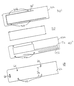
Figure 4 shows still another embodiment of the present
invention which is utilized for producing individual lamp
structures, as opposed to a plurality of lamp strips described
and shown, for example, in Figures 1-3, 7 and 14.
The film 30' of Figure 4 differs from the film 30 shown
in Figure 1 in that a substantially J-shaped busbar 36' is
formed on the underside of the plastic substrate 32a. Film
3~' further may also include an adhesive layer, not shown for
1;~145~(,
24
purposes of simplicity, but which is substantially the same as
adhesive layer 34 shown in Figure 1.
Film 40'' of Figure 4 differs from films 40 and 40' of
Figures 1 and '7, respectively, in that the back electrode 44'
is provided with an integral trace or tail T2 electrically
connected with the back electrode and extending toward the
right-hand edge 42a of plastic substrate 42. A tail T1 is
arranged in spaced parallel fashion with tail T2. Film 40''
may be further provided with an adhesive layer, not shown in
Figure 4 for purposes of simplicity, but which is
substantially the same as the adhesive layer 46 employed, for
example, in the embodiment of Figure 1.
The substrates 32 and 42 of films 30' and 40'' are
further provided with alignment holes 32b and 42b,
respectively, pairs of said alignment holes preferably being
arranged on opposite sides of the electrodes 36' and 4~' in
the manner shown. The films 20, 30' and 40'' are positioned
upon an assembly jig 60 comprising a surface 62 having a
pluralit~ of registration pins 64 adapted to extend through
the registration openings 32b and 42b in order to place layers
30' and 40'', and specifically the busbar and back electrode,
in proper registration. Film 40'' is placed upon surface 62
with openings 42b each receiving one of the associated pins
64.
Film 20 (see Figure 1) is then placed upon the top
surface of layer 40'' so that its left-hand edge 20a rests
against stop 66 provided upon surface 62. The width W of
layer 20 is preferably just slightly less then the distance D3
between the pins 64 arranged along opposite longitudinal sides
of surface 62. Positioning of film 20 relative to layer 40''
(as well as layer 30') is not critical for the reasons set
forth hereinabove so long as film 20 is substantially
coextensive with the front and back electrodes 36'and 44'.
1 :~1 4~
Finally, film 30' is placed upon film 20 so that each of
its openings 32b receives one of the associated pins 64. The
films are now in proper alignment.
Figure 4a shows a top plan view of the films 30', 20 and
40'' mounted upon the alignment pins and in proper registry.
Tail T1 electrically engages the right hand portion 36a' of
busbar 36'. If desired, the films may be placed upon the
alignment pins in the reverse order, i.e. film 30' first; then
film 20, then film 40''. The films are laminated together
utilizing, for example, a platen provided with alignment
holes, each receiving one of the associated alignment pins 64.
The platen may be pressed downwardly upon the assembly.
Either the platen or surface 62 may be heated by suitable
heating means to a temperature, preferably in a range between
about 100 and about 350F to activate the heat sealable
adhesive or resin. The above procedure may be semi- or fully
automated for a continuous web operation.
Noting Figure 8, films 30' and 40'' of Fig. 4, may be
elongated webs provided with alignment openings 32b, 42b
arranged in the longitudinal sides of the elongated webs at
regularly spaced intervals. One of the rollers 56, 58 (see
Figure 6) may be provided with alignment pins 58a, for
example, which enter into cooperating openings (not shown) in
roller 56 and which enter the alignment openings in films 30',
40'' to maintain the busbars and back electrodes in registry.
The light emitting film 20 (Figure 8) has a width slightly
less than the spacing between the alignment pins. The nip may
be heated to activate heat sealing resin(s). The finished
lamp assemblies may then undergo a die cutting operation,
which may also be an assembly of cooperating rollers located
downstream relative to the laminating nip and the drying
station.
Alternatively, the films may be advanced by pinch rollers
engaging the opposite longitudinal sides of the films to be
26 1 31 ~5~',
laminated. Optical means (not shown) can detect registration
marks and halt feeding of the films through the laminating nip
if a misregistration condition is detected.
The films may be sealed in the above manner and then die
cut. The die cutting may be either a separate process step or
may be incorporated in the heat sealin~ operation, for
example, by providing a suitable groove in surface 62 (Figure
4) for receiving a cutting edge, said cutting edge being of a
rectangular shape for cutting away the unused outer marginal
portion of the laminated structure. The traces or tails,
aligned on the same side of the back electrode 44'', provide
optimum connector contact.
The laminant of Figs. 4, 4a and 8 totally seals the
phosphor, busbars, and back electrodes between plastic
substrates 32 and 42 to protect these layers from
contamination and oxidation. Traces T1 and T2 are preferably
terminated at a point slightly inward from the edge El of the
laminated structure shown in Figure 4a in order to likewise be
totally sealed. A puncture connector can then be aligned and
pressed into position. The connector may, for example, be a
Berg Clincher (TM) connector produced by DuPont.
Alterna-tively, pressure-type or insertion-type connectors may
be employed as suitable alternatives.
The technique just described eliminates the need for
separate conductive -tails employed in prior techniques, which
are prepared in a separate operation, and which further
require the application of an adhesive to be applied to and
properly adhere the metal-to-metal contacts between the
laminated structure of Figure 4a and the aforementioned
conductive tails.
The individual electroded films 30' and 40'' may be
produced one-at-a-time as in Fig. 4, or, alternatively, a
plurality of the electrodes may be produced using a large
27 l 31 ~5Q6
plastic substrate having a plurality of electrode patterns
arranged upon the sheet in a regular fashion as shown in
Figure 8. These patterns can then be individually cut out and
assembled in the manner shown in Figures 4 and 4a.
Alternatively, the sheets containing a plurality of the
busbars and electrodes, respectively, may first be assembled
together using a registration and alignment technique as shown
in Figures 4 and 4a, whereupon all of the individual lamp
structures are laminated in one operation and thereafter are
separated into individual lamps by a cutting operation. The
films 30' and 40'' may be aligned using the alignment pins and
cooperating alignment holes of Figures 4 and 4a, or an optical
alignment technique if desired.
The advantages of the system employing films 30' and 40''
in the embodiment shown in Figures 4 and 4a, as well as the
embodiment shown in Figures 1-3 reside in the fact that any
misregistration or any other errors encountered in the
production of films 30 and 40 do not result in the expensive
layer 20 being discarded due to the formation of a defective
or misaligned busbar and/or electrode layer.
A latitude of modification, change and substitution is
intended in the foregoing disclosure, and in some instances,
some features of the invention will be employed without a
corresponding use of other features. For example, the
technique of Figures 4 and 4a may be used to laminate the
films shown in Figures 7 and 14. Accordingly, it is
appropriate that the appended claims be construed broadly and
in a manner consistent with the spirit and scope o~ the
invention herein described.