Note: Descriptions are shown in the official language in which they were submitted.
1 3 1 ~ 9 ~ ~
CONTINUOUS PHASE SHIFT MODULATION
SYSTEM WITH IMPROVED SPECT~UM CONTROL
,~.,
BACKGROUND C)F THE INVENll:CON ~ `
This invention relates to data communication systams
and, more particularly, to continuous phase shift
modulation systems.
Continuous phase shift modulation ~somekimes referre~
to as minimum frequency shift keying) is a known and
commonly used technique for modulating digi~al data onto
a radio Xrequency carrier `wav for transmission and
subsequent reception. The ~aseband representation of a
10 continuous phase shift modulation signal is comprised of
~ an in-phase and a quadrature component, each of which is
:~ composed of a continuous sequence of half-cosina pulses
of varying polarities.: ~he quadrature pulses are time
offset ~rom the in-phase pulses by 90, so that the
resulting vector sum amplitude i~ a constant. An
advantageou result of this technique is that the
modula~ion affeats only the phase of the carrier signal
and not the amplitude. This allows for the use vf highly
non-linear radio frequency transmitter power amplifiers,
thereby reducing cost and size and increasing efficiency.
In order to facilitate the explanation that follows,
the logical relationship between incoming data bits and
tha in-phase and quadrature pulses has been simplified
from that usually employed in practice. This
~ 3 ~
simplification is only for descriptive purposes and is
not intended to limit the scope of this invention.
In a continuous phase shi~t modulation system, the
polarity of each in-phase pulse is determined by
successive even incoming data bits and the polarity of
each quadrature pulse is determined by successive odd
incoming data bits. Accordingly, when successive
alternate incoming data bits have the same value,
adjacent half-cosine pulses in a component will have the
same polarity. This results in a sharp discontinuity at
the juncture between these two adjacent pulses. The
discontinuity is rich in high frequency components,
resulting in spectrum spreading, which is an undesirable
attribute. It is known that filtering can improve
spectral roll off, but filtering introduces amplitude
modulation which then requires hard limiting as a final
operation to re-establish the constant amplitude
characteristic o~ the original continuous phase shi~t
modulation signal. However, the use of limiters
introduces excessive complexity and cost, and even then
it is difficult to achieve aclequate limiter performance.
It is therafore an object of the present invention to
provide improved spectrum control in a continuous phasa
shift modulation system.
It is another object of this invention to provide such
improved spectrum control while strictly maintaining the
constant amplitude characteristic of the signal, thereby
eliminating the need for hard limiting.
SU~MARY OF THE INVENTION
The foregoing and additional objects are attained by
providing an improved modulation technique for a
continuous phase shift modulation system. The inventive
method comprises the step of determining in advance for
each o~ the in-phase and quadrature components whether
successive pulses are to have the same or different
polarity. If successive pulses in a component are to
~ 3 ~
have the same polarity, a continuous transition
modulation signal between the successive pulses is
provided in place of adjacent portions o~ the successive
half-cosine pulses. The modulation signal of the other
component is then adjusted during the time o~ the
continuous transition modulation signal so as to maintain
the desirable constant amplitude characteristic.
In accordance with an aspect of this invention, a
system for implementing the inventive method includes a
skorage device for stsring a plurality of modulation
signal se~ments which are selectively retrieved for
modulating the carrier after determining whether
successive pulses are to have like or different polarity.
BRIEF DESCRIPTION OF THE D}~AWINGS
The foregoing will be more readily apparent upon
reading the ~ollowing description in conjunction with the
drawings wherein:
FIGS. lA-lE illustrate a sequence of binarv data bits
and modulation signal waveforms useful in understanding
this invention;
FIG. 2 is a table o~E formulas for generating
modulation signal segmant~; in accordance with this
invention: :
FIG. 3 is a block diagram of an illustrative
arrangement for implementing this invention;
FIG. 4 is a waveform for an alternate embodiment of
this invention; and
FIG. 5 is a block diagram of an illustrative
: arrangement for implementing the alternate embodiment of
this inventîon.
DETAILED DESCRIPTION
Referring now to the drawings, FIG. lA illustrates an
exemplary ~equence of binary data bits spaced at a fixed
time interval T. ~hus, at time to there is a data bit of
binary value 0; at time t1 there is a data bit of binary
13~9~
value 0; at time t2 there is a data bit of binary value
l; at time t3 there is a data bit of binary value 1; at
time t4 there is a data bit of binary ~alue 1; etc. The
times t~, t~, t2, etc, are separated by a time interval
T.
As discussed above, in a continuous phase shift
modulation system, the modulation signal includes an in
phase and a quadrature component, each of which is
composed o~ a continuous sequence of half-cosine pulses
of varying polarities. The polarity of each in-phase
pulse is determined by successive even incoming data bits
and the polarity of each quadrature pulse is determined
by successive odd incoming data bits. FIG. lB
illustrates a conventional in-phase component of a
continuous phase shift modulation signal based upon the
sequence of data bits shown in FIG. lA, and FIG. lC
illustrates the corxesponding conventional quadrature
component of a continuous phase shift modulation signal
based upon the se~uence of data bits shown in FIG. lA.
Thus, as shown in FIGo lB, since the data bit at the time
to has the binary value 0, the half~cosine pulse in the
in-phase ~ignal surrounding the time to is negative.
Since the data bits at the times t2 and t4 both have the
binary value 1, the half-cc~sine pulses surrounding the
times t2 and t4 in the in-phase signal are ~oth po~itive.
Similarly, looking at the quadrature component signal
illustrated in FIG. lC, the half-cosin2 pulse surrounding
the time t1 is negative because the binary value of the
~ata bit at the time t1 is ~; and the half-cosine pulse
surrounding the time t3 iS positiv~ because the binary
~alue of the data bit at the time t3 is 1. The in-phase
and quadrature co~ponent sîgnals satisfy the condition
that at any given time, their vector sum is a constant.
In other words, the sum of the squares of the component
signal values is ~onstant. The undesirabls attribute of
spectrum ~preading which the present invention seeks to
overcome occurs at the juncture of the two positive half-
1 3 ~ 7
cosine pulses in the in-phase component illustrated in
FIG. lB.
In accordance with the principles of thi~ invention,
in place of the conventional continuous phase shift
modulation sharp V~like discontinuity shown in FI~. lB at
time t3, the continuous transition bridging waveform
shown in FIG. lD is utilized in the region t3 + 1/2 T.
Illustrativaly, this bridging function is the previous
~ 45 cosine segment inverted and biased to retain
continuity of the waveform and its first derivative. In
order to maintain constant the vector sum amplitude of
the in-phase and ~uadrature components, the quadrature
component signal illustrated in FIG. lE must be modified
within the time interval t3 ~ 1/2 T to compensate for the
increased value of the in-phase component signal during
this time interval. Thus, the value of the quadrature
component signal during that time interval is chosen to
be the square root of the vector sum ampli~uds squared
less the in-phase component value squared. For the
purposes of further discussion, the vector sum amplitude
will be considered to be unlty.
FIG. 2 is a table showing illustrative formulas for
generating the in-phase and quadrature component
modulation signal segments according to this inventionO
In that table, the formulas with the s~bscript 1 relate
to the unmodi~ied waveform segments, whereas those with
the subscript 2 relate to the modified waveform segments.
According to the present invention, the appropriate next
waveform segment for the in-phase and quadrature
components must be salected and generated at each 45
point, i.e., at t = tj -1/2 T for the ith bit. At these
points, tha waveform amplitude will always be ~ Cos 45
= + O.707. A total of eight waveform segments are
required, the unmodified peaX and ~alley waveform
sesments P1 and V1, the modified peak and valley waveform
segments P2 and V2, and the corresponding negative values
o~ each. These waveform segments satiæfy the condition
~31~9~7
that at any given time p~2 + V~2 = 1 and pZ2 + V22 = 1.
Which P (peak) waveform is chosen is dependent upon
selection of the appropriate V ~valley~ waveform. Thus,
for a particular signal component, i~ two successive
pulses have the same polarity, then a V2 waveform is
chosen as a continuous transition bridging segment. This
dictates that a P2 waveform be chosen for the other
componPnt during that time interval.
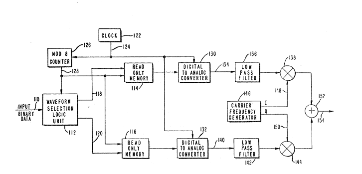
FIG. 3 is a block diagram showing an illustrative
system implementing this invention. As shown therein~
the input sequen e o~ binary data bits i5 receivad over
the lead 110 and applied as an input to the waveform
selection logic unit 112~ The function o~ the waveform
selection logic unit 112 is to examine the sequence
appearing on the lead:110, divide this sequence into two
subsequences of the alternate bits, one for each o~ the
in-phase and quadrature component signals to be
generated, and determine within each of these
subsequences whether successive data bits have the same
or dif~erent values. Read only memory 114 and read only
memory 116 are provided ~or storing data to reconskruct
the wave~orm signal segments fcr the in-phase and
quadratuxe component signals. Illustratively, the read
only memories 114 and 116 are identical, since ~he
formulas for the component waveform signal segments are
: the same (see FIG. 2), and each of the waveform signal
segments is ~tored as eight samples, wîth each sample
being represented by an eight bit word of memoryO The
eight words for each of the waveform signal segments are
stored in successive addressabIe locations. Accordingly,
when it is desired to retrieve 02le o~ the signal
segments, the address of the first sample word is
developed and then that word and the next seven words are
accesse~. :
Accordingly, the wave~orm selection logîa unit 112
determines which ~egments are to be retrieved ~rom the
read only memory 114 and the read only memory 116 and
`
.
~311 ~9~
provides on the leads 118 and 120 the addresses of the
first sample word o~ the desired segments. A clock 122
is provided which places a clock signal on its output 124
at a frequency corresponding to the frequency of the
input sequence of binary data on the lead 110 times the
number of samples per waveform segment (eight times in
this example). Thus, the clock 122 operates at a
frequency of 8/T~ The clock signal on the lead 124 is
provided as a synchronizing input to the modulus eight
counter 126 which divides the interval T into eight equal
subintervals. The output o~ the counter 126 on the lead
128 is utilized by the logic unit 112 and the read only
memories 114 and 116 to step through the remaining sample
words of the selected segments a~t~r the addresses of the
first sample words of the segments are applied to tha
leads 118 and 120.
The timing v~ the se7ection and generation of the
se~ments is as follows. For bit i, prior to tl -1/2 T,
the logic unit 112 chooses the next in-phase and
quadrature component waveforms and at time tj -1/2 T
places an address on the leads 118 to the read only
memory 114 and places an address on the leads 120 to the
read only memory 116. The counter 126 then steps throu~h
the eight sequential words of the waveform samples,
before the process repeats beginning at time tj +1/2 T =
t~ 1/2 T-
The output of the read only memory 114 is provided asan input to the digital to analog converter 130 and the
output of the read only memo~y 116 is provided as an
input to the digital to analog converter 132. The
converter 130 takes each eight bit sample word and
con~erts it to an analog signal on the lead 134, which is
applied to low pass filter 136. The low pass ~ilter 136
receives the sequence of analog signals on the lead 134
and provides therefrom a smoothed waveform signal. The
smoothed wave~orm signal is then applied to multiplier
138. The multiplier 138 can be implemented with a
conventional RF mixer component. Similarly, the analog
signal output of converter 132 on the lead 140 is applied
to low pass filter 14~ and then to multiplier 144. The
outputs of the filters 136 and 142 correspond to the
wave~orm~ shown in FIG. lD and lE, respectively.
Carrier frequency signal generator 146 generates the
radio frequency carrier signal and provides an in-phase
compon~nt of that signal on the lead 148 having a
relative phase o 0 and a quadrature component of that
signal on the lea~ 150 having a relative phase of 90.
The in-phase component on the lead 148 is applied as an
input to the multiplier 138, where it is multiplied by
the in-phase modulation signal output of the low pass
filter 136. Similarly, the quadrature component on the
lead 150 is multiplied by the guadrature modulation
signal output of the filter 142. The modulated carrier
component signals are then applied as inputs to the adder
15Z, whose output on the lead 154 is the continuous phase
shift modulation outputO
Although a cosine function for the bridging segment V2
has been disclosed, other functions are possible. The
cosine function disclosed in FXG. 2 provides continuity
o~ the signal and its fir~t derivative. If it were
desired to have in addition a continuous second
derivative, a guartic polynomial of the form:
V2(a) = -0~3257a4 ~0.852a2 +0.3055 forlal <~r/4;
where a = (qr/2)~t/T)
could b~ utilized.
More generally, various V2 f~nctions can be constructed
which provide continuity up to the Nth derivative. As N
increases, the rate of frequency spectrum r~lloff at high
frequencies increases. In this way, the spectrum can be
optimized to meet desired performance characteristics.
As an alternative to the generation of the final RF
waveform by means of RF carrier frequency generator 146
and multipliers 138 and 144 as previously described, the
modulated signal on the lead 154 can be generated more
directly by u~e o~ high speed read only memories and
digital to analog converters.
To generate modulated carriers at a desired center
frequency F, each read only memory is accessed at a rate
of 2F with successive outputs alternating between
positive and negative values. The magnitude of these
samples should be chosen to be the appropriate stored
time samples of the desired waveform segments as
described previously from the wave~orm selection processO
These samples are supplied to a digital to analog
converter and its output in turn is provided to a
bandpass ~ilter centered at frequency F to generate a
modulated carrier simiIar to the output of mixer 138 in
FIG. 3. A similar process is used in the lower channel
for the quadrature signal. Although a rate of 2F has
been described, it is possible to access the memory at a
rate which is a multiple of 2F~ In this case, there
would be a number o~ successive outputs o* the ~ame
polarity alternating with that number o~ successive
outputs of the opposite polarity, the number being equal
to the multiple of 2~ of the sampling rate.
FIG~ 4 illustrates this approach for the wave~orm
corresponding to the portion of the baseband waveform in
FIG. lB between the time~ t1 and t3. The vertical lines
represent the samples accessed from the read only memory
and the modulated sine wave shows the output of the
digital to analog converter after it has been passed
through a bandpass filter centered at tha desired
fre~uency F. For this illustrative exampIe, there are
eight samples per bit interval T and the frequency F i~
1/2T. However, in a practical application, the frequency
F would be many times greater than the bit rate.
FIGo 5 illustrates an implementation of this alternate
approach. The ~igital hardware through the digital to
analog converters i~ identical to FIG. 3 except for the
values storad in the read only memories and tne frequency
o~ the clock. The outputs of the converters 130 and 132
~L31~7
are applied to bandpass filters 156 and 158,
respectively~ To accomplish the 90 phase shift between
the in-phase and guadrature channels, the outputs of the
filters 156 and 158 are combined by means of a quadrature
hybrid cirouit 160. This is a conventional RF component
which per~o~ms a 90 relative phase shift between the two
input signal and provides as its output on the lead 162
the sum of these two components. The output 162 of the
quadrature hybrid circuit 160 is equivalent to lead 154
of FIG. 3.
The desired phase relationship can also be
accomplished without the quadrature hybrid circuit 160 by
of~setting the digital clock phases of the quadrature
channel to delay the output of the diyital to analog
converter 132 by the equivalent of 9o. The simple
addition of the two channel outputs will then provide the
desired final output without the need for the quadrature
hybrid circuit 160.
Accordingly, there has b~en disclosed a continuous
phase shift modulation syst:em with improved spectrum
control. The improved spectr~m control results from the
elimination of the sharp discontinuity at the juncture
between adjacent pulses of the same polarity. It is
under~tood that the above-described embodiments are
merely illustrative of the application of the principles
o~ this in~ention. Numerous other embodiments may be
devised by those skilled in the art without departing
from tha spirit and scope of this invention, as defined
by the appended claims.