Note: Descriptions are shown in the official language in which they were submitted.
YO987-10~
1 3 1 499 1
COMPLEMENTARY METAL-OXIDE-SEMICONDUCTOR TRANSISTOR
AND ONE-CAPACITOR DYNAMIC-RANDOM-ACCESS
MEMORY CELL AND FABRICATION PROCESS THEREFOR
BACKGROUND OF THE INVENTION
Field of the Invention
The present invention relates to a semiconductor
memory using complementary
metal-oxide-semiconductor transistors and a
storage capacitor, and more particularly to a
structure and fabrication process for a
random-access-memory cell for dynamic operation
for large scale integrated circuit technology.
Description of the Prior Art
U.S. Patent 4,633,438 issued Dec. 30, 1986 to Kume
et al, entitled "STACKED SEMICONDUCTOR MEMORY",
describes a 3-transistor random access memory for
dynamlc operation, in which one of the transistors
is stacked on the other transistor. A transistor
for writing is disposed on a transistor for
reading, and one of its terminals is used in
common with the gate electrode of a transistor for
judging data. The other terminal is connected to
one of the terminals of the transistor for read-
ing.
A memory cell capable of extremely large scale
integration can be obtained using stacked comple-
mentary FETs, wherein the two FETs are driven by
YO9-~7-103 2 i 31 4~'31
overlapping wordlines; however, -the word].ines are
separately drlven for read and wri.te operations, rather
than simultaneo~lsly driven w:i.tll complementary signals as
in the present lnvention.
U.S. Patent 4,271,488 issned Jarm 2, 1981 to Saxe
entitlecl "HIGH-SPEED ACQUISITION SYSTEM EMPLOYING AN
ANALOG MEMORY MATRIX", describes a hlgh-,speed acquisition
system employing an analog memory ma-trix in which
sample~hold elements connectecl to an analog bus are
arranged in rows and columns to :Eorm an M x N matrix.
The system ls operable ln a fast in - slow out mocle, and
the analog memory matri.x may be implemented on a single
integrated-circuit semiconduc-tor chip . The analog memory
comprises cells containing sample/hold circuits. Typical
sample/hold circuits are shown in the drawings of U.S.
Patent ~,271~488, particularly FIG. 2, including FIG. 2C
which shows a complementary FET switching means.
However, the complementary drive signals are obtained
within the cell by means of inverter 54 and AND gate 52,
and this patent does not show or teach the use of
complementary wordlines for provi.dlng lhe complementary
drive signals as set or-th in the present invention.
U.S. Patent 3,701,120 issuecl Oct. 2~, 1972 to
Charters et al, entitled "ANALOG CAPACITOR MEMORY WITH
SLOW WRITE-IN AND FAST NONDESTRUCTIVE READ-OUT" describes
an analog memory capable of write-i.n at a relatively low
rate and independent, nondestructtve read-out at a
relatively high rate. A si.ngle write-in and read-out
address logic is
YO987-103
`- . 131~q91
provided for as memory units are desired~ Each
memory unit includes a matrix of sample and hold
microcirCuits~ each having an external storage
capacitor, an isolation amplifier and independent
input and output analog swi-tching in response to
vertical and horizontal write-in and read-out
addressing.
U.S. Patent 3,457,435 issued July 22, 1969 to
Burns et al, entitled "COMPLEMENTARY FIELD-EFFECT
TRANSISTOR TRANSMISSION GATE", describes a circuit
wherein a pair of field-effect transistors of
opposite conductivity type have their source-drain
paths connected in parallel. Signals of opposite
polarity sense are applied at the gates of the
transistors to bias both on or both off simultane-
ously. The gate comprising complementary FETs is
driven by two complementary signals as shown in
FIG. 4, in order to eliminate the drop in trans-
mitted voltage due to the threshold voltage of a
single FET. This patent does not disclose usage
within a DRAM cell.
Patent EP 175-378A of Fujitsu LTD shows
three-transistor cell DRAM structure which has
read and write select lines combined into one line
connected to gates of both read and write select
transistors. A write selector transistor is
disposed over a read select transistor, the two
being separated by an insulator layer and sharing
a drain region. A storage transistor is formed on
a silicon substrate in the same level as the read
select transistor. Channel regions of the two
yo987-103
1 31 4q91
transistorS are connected to one another and each
is used as a diffusion (source or drain) region of
the other two transistors.
Write and read select lines may be combined into a
single control line or a write/read select line.
Here gate electrodes of the read and write select
transistors are connected to the write/read select
line and are distinguished by having different
threshold voltages.
Other references include U.S. Patents 4,434,433;
4,308,595; 4,203,159; 4,044,342; 3,919,569 and IBM
Technical Disclosure Bulletins Vol. 23, No. 10,
Page 4620 and Vol. 18, No. 3, Page 649.
SUMMARY OF THE INVENTION
An object of the present invention is to provide a
complementary MOS one-capacitor dynamic RAM cell
which operates with a non-boosted wordline without
a threshold loss problem~
Another object of the present invention is to
provide a CMOS one storage capacitor DRAM cell
that incorporates both n- and p~type transfer
devices connected to the storage capacitor.
A furthe~ object of the present invention is to
provide a true CMOS DRAM cell with two complemen-
tary transistor devices having gates controlled bycomplementary wordlines.
YO987-103
1 31 ~qql
The foregoing and other objects, features and
advantages of the invention will be apparent from
the following more particular description of the
invention as illustrated in the accompanying
S drawings.
BRIEF DESCRIPTION OF THE DRAWINGS
FIG~ 1 is a schematic circuit diagram of a CMOS
memory cell according to the principles o the
present invention.
FIG~ 2 is a schematic cross-sectional illustration
of the structure of a CMOS memory cell according
to the principles of the present invention.
FIGS~ 3 and 4 are schematic cross-sectional
illustrations of the structure of the CMOS cell of
FIG~ 2 at certain steps within the fabrication
process therefor.
FIGo 5 is a schematic cross sectional illustration
of another embodiment o~ a CMOS memory cell
according to the principles of the present inven-
tion.
DESCRIPTION OF THE PREFERRED EMBODIMENTS
In integrated circuit technology employingdynamic-random-access-memory (~AM) cells, as the
DRAM density increases, it is important to scale
down the area occupied by the DRAM cells, such as
the one-transistor and one-capacitor DRAM device.
YO~87-103
1 31 4q~1
A general dilemma in scaling down the transfer
device in the DXAM cell is that in order to
minimize the leakage throuqh an l-offl' device, it
is desirable to have a higher threshold voltage;
but conversely, in order to maximize the stored
charge and to obta.in a higher charge transfer
rate, it is desirable that the threshold voltage
be small. The conventional way of using a boosted
wordline to avoid this problem becomes more
difficult as the device dimensions are scaled
down; for example, the reduced breakdown voltage
of the scaled down device limits the possible
boosted wordline voltage level. It is important
for DRAMS, therefore, to design a new cell which
allows usiny a non-boosted wordline, but without
suffering the ~hreshold loss problem as described.
The present invention provides a Complementary MOS
one-capacitor DRAM cell (CMOS-lC cell) which
overcomes the described problem. A circuit
schematic of an embodiment of the new cell is
shown in FIG. 1. The difference from the conven-
tional one-transistor DRAM cell is that instead of
having only a single type of tran~fer device
connected to the storage capacitor, there are both
an n- and a p-type transfer device in each cell,
for example, devices 10,12 and 14,16 in FIG. 1.
The gates 18,22 and 20,24 of these complementary
devices are controlled by complementary word lines
26 and 28, respectively. At standby, the wordline
26 is low which turns off n-type devices 10,14 and
the complementary wordline 28 i5 high which turns
off p-type devices 12,16. For cell 38 which is
YO987-103
1 3 1 ~99 1
comprised o~ the transfer devices 10 and 12, and
the storage capacitor 30, the charge is stored on
the capacitor 30, isolated from the bitline 34 at
standby. When the cell is selected, wordline 26
goes high and complementary wordline 28 goes low
to turn on both devices 10 and 12. Complementary
devices 10 and 12 comprise a CMOS pass gate,
having no threshold loss. As a result, there is
no need to boost the wordline voltage level in
order to store the full voltage, either the full
power supply voltage VDD or zero volts. As a
result, the total sense charge can be read from,
or stored into, the capacitor 30 through the
bitline 34 in a full-VDD amount, i.e~, with no
threshold loss.
There are several advantages of the described
cell: (1) It does not suffer the threshold voltage
loss for the charge transfer, even though the
wordline voltage level is not boosted, because
either VDD or zero can be fully transferred
through the PMOS or NMOS, respectively; (2) the
signal development is faster because both devices
conduct most of the time during charge transfer;
and (3) because the cell does not suffer threshold
loss and has high charge transfer rate, the
transfer devices can be designed to have large
absolute values of the threshold voltage in order
to suppress leakage.
The present invention provides a fabrication
process which overcomes the technological
difficulty of how to achieve both PMOS and NMOS
YO987-103
1 3 1 499 1
devices within the area on the integrated circuit
presentlv occupied by a single device. The
present invention also provides a novel cell
structure for the CMOS-lC cell, which occupies
about the same area as the one-device cPll.
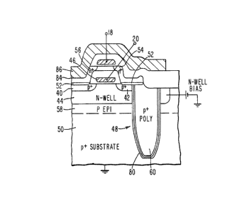
FIG. 2 shows a schematic o the cross section of
this new cell structure. The CMOS-lC cell of FIG.
2 includes a PMOS device having p~ drain and
source regions 40,42, respectively, in n-well 44,
and a gate 46. The cell also includes a trench
capacitor 48 in a p~ substrate 50. The trench
capacitor 48 is connected to the p+ source region
42 of the transfer device through a layer of
interconnection 52 called the strap. The strap
material, for example, may be titanium silicide,
titanium nitride/titanium silicide, or cobalt
silicide. Above the PMOS transfer device is the
other, n-type, (NMOS) transfer device including
source and drain regions 54,56,-made in a SOI
(silicon-on-insulator) film. Because the strap 52
is conductive to both p- and n-type material, the
source and drain regions 42,40 and 54,56 of both
NMOS and PMOS devices are connected. Gates 18 of
the NMOS device and 20 (also referred to as 46) of
the PMOS device are connected, respectively, to
wordlines 26 and 28 which are connected to their
own individual wordline drivers at the end of the
array. The NMOS device and PMOS device of FIG. 2
correspond to devices 10 and 12 of FIG. 1,
respectively, and operate as previously described.
YO987-103
1 3 1 ~99 1
A process to fabricate the cell structure of FIG.
2 will be described. Although the process will be
described for one cell, it should be understood
that the process applies to the fabrication of a
plurality of cells in a dense array. The process
consists of the following steps:
Step (1) With a p epitaxial layer 58 disposed on
a p+ semiconductor substrate 50, Reactive Ion Etch
(RIE) a 5 to 6~m deep trench into the p epi layer
58 and p+ substrate wafer 50O (FIG. 3)
Step (2) Form a composite oxide/nitride/oxide
storage insulator 80 on the walls of the trench.
(FIG. 3).
Step (3) Fill trenches with p+ polysilicon 60 and
planarize.
Step (4) Form a retrograde n-well 44 by two
phosphorous implants: a surface implant and a deep
implant using 1.6 MeV energy.
Step (5) Grow local oxide isolation region 82.
Step (6) Adjust the threshold voltages of PMOS
and peripheral-circuit NMOS devices by a single
boron implant.
Step (7~ Grow gate oxide and deposit n+
polysilicon gate material 46 and oxide film 62
over the PMOS gate and pattern.
YOg87-103
1 31 ~991
Step (8) Form oxide spacer on gate electrode
edges.
Step (9) Implant phosphorous and boron to obtain
graded source/drain junctions for PMOS and NMOS
devices, respectively.
Step (10~ Open surfaces of source/drain regions
42,40 for silicide 52 formation wherein the gate
46 is still protected from said silicide by thick
insulator 62 (FIG. 3).
10 Step (11) Form a lightly doped p-type silicon -.
film 64 over the silicide, and isolation regions,
wherein alternatively, said film 64 (lla~ is
deposited in polycrystalline structure and
recrystallized by beam annealing; (llb) film 64 is
deposited, in polycrystalline structure and the
grain boundary traps are inactivle by hydrogen
passivation treatment; lllc) an ,amorphous film 64
is deposited and because of crystalline seeds of
silicided p~ source/drain regions~ the amorphous
film can be converted to single crystal after
thermal treatment; or (lld) film 64 is deposited
in polycrystalline structure and the p-type doping
level is adjusted to g.ive a high threshold volt-
age, which can be used to minimize the device
leakage.
Step (12) ~efine the N~OS active area and grow
thin gate oxide.
YO987-10;3
1 31 4~1
Step (13) Adjust n-chann~l threshold voltages by
a boron implant.
Step (14) Deposit n+ polysilicon gate material 18
and pattern. Form oxide spacer on gate electrode
edges.
Step ~15~ Implant arsenic dopants to obtain nt
source/drain junctions 54,56 for n-channel trans-
fer devices and grow oxide to cover the device.
Step (16) Deposit blanket glass film and reflow.
Step (17) Etch contact holes 84, deposit and
pattern metal level 86.
This results in the cell structure shown in FIG.
2.
Another embodiment o a structure of a CMOS-lC
cell according to the present invention is depict-
ed in FIG. 5. In this idealized structure, the
CMOS pass gate is comprised of the PMOS device 72
and the NMOS device 74; both devices 72 and 74 are
vertical transistors, fully insulated from sur-
rounding conducting materials, except for contactsto the bit line 73 and a connecting silicide or
metal strap 75. The entire cell, including the
poly gates 77 and 78, which are interconnected
with the gates o~ other cells to form complementa-
ry wordlines, can be built in trenches 68 etchedinto a conductive substrate 70 covered by a thick
insulator 79. The storage capacitor consists of
~0987-103
1 31 ~q~ 1 -
12
poly electrode 90, thin oxide dielectric 71, and
the plate 70. The poly electrode 90 is intercon-
nected to the device diffusions by the conductive
strap 75.