Note: Descriptions are shown in the official language in which they were submitted.
1315~15
.
-- A FIELD-EFFECT DEVICE WITH A SUPERCONDUCTING CHANNEL
.
OESCRIPTION -
. .
The invention concerns a field-effect device such as a field-effect transistor
(FET) that can be utilized in electronic circuitry and that is suited for use inIntegrated circuits. The device comprises a layer of superconducting material
forming the channel through which a current of charge carriers may Slow, a
pair of terminals for feeding a current through the channel, and a control gate
for applying an electric field to the channel, the field affecting the charge
carrier density within the channel zone under the gate.
.. .
Field-effect transistors are well known and find wide applications, for example
as a swltchlng device, In memories or In logic circuitry. FET's with
semiconductor channels, mostly consisting of silicon (Si) and, more recently, ofgallium arsenide (GaAs), have become an established element in data
processing systems. Great progress has been made in designing fast and
small dimension devices, down to sub-micron structures, that lead to high
package densities and thus to high speed integrated circuits. There is,
however, a need for stlll faster circuits.
Investlgatlons have shown that sllicon and gallium arsenide semiconductor
devices can operate optimally at a temperature of about 77K, the liquid-
nitrogen temperature range. This optimum performance at low temperatures,
together with the fact that the resistance of metallic wirlng or device
connections decreases with decreasing temperature, make low temperature
systems attractive.
Regard.ng the development of low temperature devices, there have been
proposals for semiconductor FET structures having superconductor source and
131~01~
2 SZ9-87012
drain electrodes and where the semiconductor current channel, due to the
so-called "proximity effect", becomes superconducting in the vicinity of the
superconductor electrodes. An article "Three-Terminal Superconducting
Devices", written by W.J.Gallagher (lEEE Trans. on Magnetics, Vol. MAG-21,
No.2, March 1985, pp 709-716) provides a brief description of such proximity
effect devices as well as prior art references. Fabrication . and operating
margins of these devices would, however, be rather critical.
Furthermore, there have been proposals for FET structures comprising a
superconductor channel. They have been described, for example, in the
following articles: "Superconducting Field-Effect Transistor" by F.F.Fang et al
(IBM Technical Disclosure Bulletin, Vol.19, No.4, September 1976,pp
1461-1462), and in "Experimental Considerations in the Quest for a Thin-Film
Superconducting Field-Effect Transistor" by A.F Hebard et al (IEEE Trans. on
Magnetics, Vol.MAG-23, No.2, March 1987, pp1279-1282).
. .
These articles describe studies on structures with a superconductor channel
having a thickness of about 10 nm. An applied electrlc field causes a slight
change in carrier density in a thin surface layer at the gate-superconductor
interface. This change in carrier density in turn results in a shift in transition
Temperature Tc in the thin layer. By applying signals to the gate, the thin layer
can be switched between "superconducting" and "normal-conducting" states.
This results in a change in channel resistance.
Since the field-induced effect does not extend deeply into the channel material,various approaches to enhance the magnitude of the effeçt have been studied
and published by A.T. Fiary and A.F. Hebard in two articles "Field-Effect and
Electron Density Modulation of the Superconducting Transition in Composite
In/lnOx Thin Films" (Physica 135 B, 198~, pp 124 - 127, Nt)rth-Holland,
Amsterdam) and "Electric Field Modulation of Low-Electron Density Thin-Film
Superconductors" (Proc. Internat. Workshop on Novel Mechanism of
Superconductivity, Berkeley, June 1987). There is another article on this
subject by M. Gurvitch et al, "Field Effect on Superconducting Surface Layers
of SrTiO3 " (Materials Research Society 1986, pp 47 - 49).
~31501~
.
3 sz 9-87-012
The drawback of these "surface effect" deivices is that the change in channel
resistance is still quite small. Even in the "switched" thin surface layer the
change is only from metal-conducting to superconducting, and in addition, the
bulk section of the channel that is not aflected by the applied field acts as a
metal-shunt. Therefore, the obtainable output signals are too small as to be
able to drive next stage FET devices.
Another drawback is that the change in Tc is rather small, i.e., operating
temperature (TOp)requirements are stringent since, for proper operations, the Tcof the thin layer has to change from "above Top " to "below Top ".
At present, the speed of integrated circuits is essentially determined and
limited by the relatively high resistance of the wiring and device connections
rather than by the devlces themselves. Further progress could, therefore, be
achieved if the wirlng could be made of superconductor material. At operating
temperatures below Tc of the superconductor material, the line resistance
would be reduced to zero and systems with devices linked by resistance-free
connections offer increased speed.
This has become feasible since the discovery of a new class of high-Tc
metal-oxide superconductors (also referred to as ceramic superconductors)
that were first described by G.Bednorz and K.A.Mueller in their article
"Possible High-Tc Superconductivity in the Ba-La-Cu-O System" (Z.Physics,
Condensed Matter, Vol.64, 1986, pp 189-193). Further developments have
resulted in metal-oxide superconductor materiais, such as YBaCuO, having a
Tc well above the temperature of liquid nitrogen. Such composition has been
described by C.W. Chu et al in an article "Superconductivity at 93 K in a New
Mixed-Phase Y-Ba-Cu-O Compound System at Ambient Pressure"
(Phys.Rev.Lett. 58, No. 9, March 1987, pp 908 - 910).
With this development, integrated circuits, cooled with liquid nitrogen, and in
which both, devices and connections consist of superconductor material are
expected to become reality provided high performance devices, e.g., effective
switching elements, can be designed. The obstacles encountered in using
hybrid semiconductor-superconcluctor techniques would be removed.
131501S
4 SZ 9-87-o 12
It is thus the main object of the present invention to provide a highspeed
superconductor field-effect device that can be fabricated using the same
technology as that used to produce the device connections and that can be
- operated as a switch at operating temperatures below the transition
temperature Tc of the superconductor material.
- The invention as claimed is intended to meet this objective and to remedy the
drawbacks of hitherto known structures. It solves the task of providing a switchhaving a high ON-/OFF-current ratio in that the thickness of the
superconductor channel is made sufficiently thin so that, when applying a
control signal of proper magnitude ~a few Volt are sufficient) to the gate, the
channel becomes completely depleted of charge carriers.
The advantages offered by the Invention are mainly that
.. .
- the devlce provides a high-performance switch element that is capable
of swltchlng from zero resistance (when superconducting) to "insulating"
(when the channel is depleted),
- it provldes high outputs sufficient to drive connected field-effect
devices, and that
- strlngent operating temperature reciuirements are avoided because the
operation does not rely on an ''Tc-shift'' effect.
In line with the main object, the device can be produced ln the same high-Tc
superconductor technology that is used in fabricating the integrated circuit
wiring and device connections.
One way of carrying out the invention is descri~ed in detail below with
reference to drawings in which
Fig.1A & 1B illustrate, in a schematic cross-section, the ON- and
OFF-states of a prior art FET that relies on surface field effects;
,
1315015
;~
s SZ 9-87-0I2
Fig. 2 is a not-to-scale cross-sectional view of a FET structure
in accordance with the invention; and
. Fig.3A & 3B illustrate, in a schematic cross-section, the ON- and OFF-states of the FET structure shown in Fig.2.
's
The inventive fleld-effect device comprises, in principle, the same basic
elements as the surface effect superconductor FET structures that have
previously been investigated and described, e.g., in the above cited article that
was published in the IBM Technical Disclosure Builetin.
Such a prior art structure and its operation are iilustrated in Fig.1A and Fig.1B.
On an insulating or semi-insulating substrate 10, a superconductor channel 11
of about 10 nm thickness is deposited and provided with source 12 and drain
13 tern inals. Gate 15 is separated from the channel by an insulating layer 14.
With properly chosen materials, at an operatlng temperature Top that is slightlyabove the transition temperature Tc of the channel material, and with no gate
voltage (Vg= 0) applied, the channel is "normal"-conclucting thus providing, in
the OFF-state of the device, a finite conductivity current path. It is however to
be noted that, because the superconductors used are metals, the conductivity
is high even in the OFF- or "normal conducting-" state. In Fig.1A, the resultingcurrent is indicated by arrows 16. The current is equally distributed over the
entlre cross-section of the channel under the gate.
As illustrated in Fig.1B, application of a non-zero voltage (V9~0) causes a
slight change in carrier density within a thin surface layer 11a of a few tenthsof a nanometer thickness near the superconductor-insulator interface. This
change in carrier density results in an increase in Tc within the very thin
surface layer, to a value above the operating temperature Top of the device,
thereby making the thin layer superconducting. In this ON-state, the device
provides a current path of very high conductivity. Arrow 17 represents the
supercurrent flowing in the now superconducting layer 11a; there is no current
flow in region 11b of the channel since it is shunted by the zero-resistance
supercondusting region 11a. The ON-lOFF-current ratio is limited because, in
'' ' . ,
13~501~
6 SZ 9-87-0 1 2
the ~FF-state, the normal-conducting channel is still conducting a rather heavy
current. Also, the current-carrying capability of the very thin channel 11a is
severely restricted by the value of the maximum current density above which
the material of the thin channel becomes normal-conducting. Such FET could
not provide a sufficient output to drive a subsequent FET. Furthermore, it's
operation would be very critical with regard to slight changes in operating
temperature.
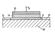
Fig.2 illustrates the generai structure of the inventive field-effect device
consisting of a channei 21 which is deposited onto a substrate 20 and provided
with source 22 and drain 23 leads as weli as with a gate 25 that is separated
from the channel by an insulating layer 24.
In a preferred embodiment, the substrate consists of strontium titanate (SrTiO ,)
on which the channel of a high-Tc superconductor material, in the example
YBa2Cu3O,, Is grown. The channel is very thin, in the order of 1 nm, and is
single crystalline and oriented so that the super-conducting behaviour is
strongest In the plane parallel to the substrate surface.
For the growth of the thin channel layer an epitaxial process is used, followed
by after-treatments such an oxygen anneal. Such techniques have, more
recently, been developed. Growth processes such as molecular beam epitaxy
(MBE), metal-organic vapor phase epitaxy (MOVPE) or chemical beam epitaxy
(~:BE) allow the growth of abrupt ir~terfaces. In addition, the low growth rate
and the precise control of the growth parameters allow to grow very thin
layers. In special modified systems, the control of the growth process can be
at the atomic level. Such techniques have, for instance, been described in
U.S.Patent 4,058,430 and in the following articles:
- "Growth and Characterization of Compound Semiconductors by Atomic Layer
Epitaxy" by M.A.Tischler et al (J.Cryst.Growth 77, 1986,pp 89-94);and
-~Atomic Layer Epitaxy" by H.Watanabe et al (Inst.Physics.Conf.Ser.No. 83,
Chapter 1, 1986, pp 1-9).
131501~
7 sz 9-~7-012
MBE-grown high-Tc superconductors have been published e.g. in
- "Growth of high-Tc Superconducting Thin Films using Molecular Beam Epitaxy
Techniques" by C.Webb et al (Appl. Phys.Lett. 51, October 1987, pp i191-1193);
and
- "Single Crystal Superconducting YBaCuO Oxide Films by Molecular Beam
Epitaxy" by J.Kwo et al (Conf. Proceed. "Novel Mechanism of
Superconducti~ity", June 22-2~, 1987, Berkely/U.S.).
A suitable method for fabricating oriented layers using an evaporation process
has been described by P.Chaudhari et al in an article "Critical-Current
Measurements in Epitaxial Films of YBaCuO Compound" (Phys.Rev. Lett. 58,
No.25, 1987, pp 2684-Z686).
,............. .
Returning now to Fig.2: On top of the channel 21 is an insulator layer 24
having a thlckness that is sufficient to make tunneling effects negligible. A
layer of 5 nm thick SrTiO3 has been chosen, this mate:rial having a sufficientlyhigh dlelectric constant. This layer can be applied in an evaporation process
such as chemical vapor deposition.
The gate 25 is then deposited on the insulator. In the here described
embodiment it is made of a high-Tc superconductor, e.g. YBa2Cu3O7, but any
ordinary metal such as gold would work as well. Where a perovskite such as
SrTiO3 is used as Insulator, the upper part of it could be made metallic either
by using a reducing ambient or by doping with Nb so that a separate
evaporation of a gate layer would not be required.
Source Z3 and drain 24 leads can consist of the same material as the
superconductor channel or of another high-Tc superconductor. An ordinary
metal may also be chosen.
Patterning of the structures can be done using conventional lithographic
and/or etching methods.
1315015
;
8 S% 9-87-012
It should be noted that the ceramic superconductor materials such as the
YBaCuO composition used in the described embodiment permit maximum
current densities (above which the material becomes normal-conducting) of up
to 107 A/cm2 . The allowed channel current ImaX can then be calculated from the
following equation
Imax = i(maX) x ( w x d )
with i(maX) = maximum current density
w = channel width
d = channel thickness
For w = 10 ~ and d = 1 nn, the calculated maximum current is 1 mA, i.e., an
operating current level that is adequate for most applications.
It is furthermore noted that the use of the very thin superconductor channel,
whlch is in the order of 1 nm, is only feasible because of the small correlationlength of about .2 nm along the crystallographic c-axis that is achievable with
the new class of metal-oxide superconductors such as the YBaCuO
composition used in the embodiment. Since superconductivity can only subsist
in layers having a thickness of at least the correlation length of the
supercon(iuctor material, channels of a convential metal-superconductor such
as lead or niobium, having correlation lengths that are at least an order of
magnitude higher than that of the metal-oxide superconductors, would have to
be much thicker. This then would prevent complete channel depletion with
reasonable gate voltages, i.e., the device could not operate as a switch as willbe described for the inventive FET structure in the following.
The operation of the superconductor FET will now be explained with the aid of
Fig. 3A and 3B. With no gate voltage V9 applied (Fig. 3B), channel 21 is
superconducting and the resistance between source 22 and drain 23 is zero. If
a voltage is applied to gate 2~ (Fig. 3A), the carrier concentration in the
channel is changed due to the field effect. With a sufficiently high gate voltage
and proper polarity (a negative voltage for electrons or a positive voltage for
holes), the extremely thin channel can, in the region underneath the gate, be
~ 3 1 ~
9 SZ 9-87-012
completely depleted of the carriers. The channel becomes insulating, i.e., the
channel resistance becomes very high.
The relation between applied gate voltage Vg and the depletion depth d is
given by the following equation:
. , ., ~
Vg = 112 ~q~ . d2 (1 + 2tld ,Es ) (2)
with q = elemental charge
n = carrier density (1 02'/cm3)
t = thickness of insulating layer Z4
e" eS, eO= dielectric constants of insulating layer material,
superconductor and air, respectively
. . .
The required gate voltage can be fairly low: With t = 5 nm and d--1 nm, the
gate voltage V9 requlred for complete carrier depletion in the channel
cross-section under the gate is about ~ Volt. In standard circuitry, operating
with signal levels of a few Volt, the described FET can thus be operated as a
switch havin~ two states: an ON-state with supercurrent flowing through the
zero-resistance channel (at V9= O), and an OFF-state where the channel is
depleted (V9 7~ O), i.e., Tt is insulating and the current is switched off.
The FET structure hereinabove described is distinct from previously known
devices in that the channel is made thin enough to permit complete depletion
of the channel cross-section under the gate, leaving no by-passing shunt. This
results In an extremely high ON-/OFF-current ratio and provides, when
operated at conventional current and voltage levels, for high output sufficient
to drlve connected FET devices.
'
Use of the very thin (1 nm) channel is feasible because
- the correlation length of the metal-oxide class high-Tc superconductor is
sufficiently low (in the order of a few tenths of a nanometer),
131~
;
Sz 9-87-012
- these high-Tc superconductors allow a high current density (107 Alcm2~ that
makes the device suitable for use in today's integrated circuits, and because
- recently developed epitaxy techniques permit the growing of extremely thin
layers (1 nm and below).
When operated as a switch, the inventive device does not rely on any Tc -shift
effect since there is no switching of the superconductor material between
"superconducting" and "normal-conducting". Therefore, operating temperature
requirements are not critical, allowing wide margins.