Note: Descriptions are shown in the official language in which they were submitted.
~315~L9
UNIVERSAL SEMICONDUCTOR C~IP PACKAGE
-
Back~round of the Inventlon
When a semiconductor chip is designed, it is
quite common to find that there is no package available
which is compatible with the chip for the purpose of inter-
facing the chip to a next level of packaging, e.g., to a
printed circuit board. Accordingly, there are literally
thousands of single-purpose semiconductor chip packages
available; even in a 40 pin design, there are likely
60 - 80 variations available.
Fabricating specialized packages for each new
chip design becomes expensive, particularly for chip
designs having 200 to 300 pads, each requiring connec-
tion to the package for signal, power, or ground.
Vnle~s the chip is properly designed for a pre-existing
package, connections by way of wire bonds or thermally
activated bonding (TAB) connections cannot be made; in
other words, if the chip has not been laid out so that
direct connections from the edges of a chip can be made
to corresponding signal, power or ground pads on the
chip package, a special package must be designed and
fabricated, resulting in present-day costs of $30,000 to
$80,000 per chip package, typically $45,000 for a
sophisticated package.
A significant problem with making the pads
located on semiconductor chip package~ available for
handling either signal, power or ground is that special
design considerations mu~t be adhered to for power or
ground paths that do not apply to signal paths. It is
not uncommon in semiconductor chip packages for signal
leads within the package to have relatively high
resistance and inductance values, e.g., a total
resistance on the order of 1 ohm and an inductance on
the order of 2 nanohenries/cm; such signal path values
are normally acceptable to the designers of most
--
1315~9
chips. On the other hand, most chip designers would
like a relatively low resistance and inductance path
between power and ground pads and corresponding next-
level-of-packaging power or ground connectors. For
example, many semiconductor chip package specifications
require a resistance value of less than 0.1 ohm, and an
inductance value in the picohenry range for power or
ground paths is frequently desirable. Accordingly, it
is normally not acceptable to simply use the electrical
paths available through what are originally designed to
be signal paths within a chip package for power or
ground connections.
These problems are solved by a semi-
conductor chip package comprising the present invention,
which permits individual pads on the package to function
either as signal, power or ground; in addition, this
selectivity is accomplished in the preferred embodiment
while attaining a typical power and ground path having a
resistance of less than 100 milliohms, typically 35 - 50
milliohms, and having an inductance of le~s than
one nonahenry.
Summary of the Invention
.
The present invention is a ~emiconductor chip
package comprising a plurality of programmable pads
located on an exterior surface of the package, each pad
being adapted for interconnection with a semiconductor
chip. The package also includes a plurality of signal
connectors located on an exterior surface of the
package. In addition, the package includes a plurality
of signal connections, each signal connection providing
an electrically conductive path between an individual
! programmable pad and a corresponding individual signal
l 35 connector. A plurality of dedicated power or ground
, .
. :
,- :
- . '~ ,
1 3 ~ 9
connectors are also located on an exterior surface of
the package. Conductive paths within the package provi-
de apparatus for selectively connecting any programmable
pad to a power or ground connector, any pad so connected
also remaining connected to a corresponding signal
connector.
Brief Description of the Drawings
Figure 1 illustrates the top layer of one pre-
ferred embodiment of the present invention.
Figure lA illustrates a typical cross sec-
tional view of a semiconductor chip package comprising
the present invention.
Figures 2-12 illustrate layer~ 2-12 of one
preferred embodiment of the present invention.
Figure 13 illustrates the top layer of an
alternate preferred embodiment of the present invention.
Detailed Descri~tion of the Preferred Embodiments
The semiconductor chip package disclosed here
is a 269 pin grid array package. However, the concept of
the present invention is applicable to other lead count
packages as well to packages of designs other than pin
grid arrays: for example, the present invention applies
equally well to chip carriers.
In one preferred embodiment, the present
invention is implsmented as shown in Figures 1-12, where
Figure 1 illustrates a top layer of the package and
Figure 12 illustrates a bottom layer of the package, the
bottom of the package containing in the embodiment
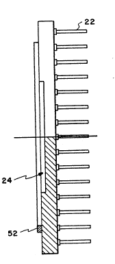
illustrated 269 pads 21, to which are connected 269 pins 22
~Figure lA) for use in connecting the package to another
device such as to a next level of packaging, e.g., a
printed circuit board.
131~
Referring to Figures 1 and lA, a semiconductor
chip or die (not shown) containing signal, power or
ground pads for connection to the present package is
placed in die cavity 24. The signal, power, or ground
pads of the chip are typically connected by wire bonds
or by TAB connections to programmable pads 26 which
surround die cavity 24 on layer 1 as shown (pads 26 are
typically confi~ured as bond pads but could also be con-
figured as flip-chip or any other pads used for chip-to-
package interconnect). In the embodiment shown, thereare 256 bond pads on layer 1 (Figure 1), and these 256
pads can be used as explained below for either power or
ground; however, as also explained below, 248 of the
pads on layer 1 (all but 8, 2 in each corner) can also
be used for signals.
Accordingly, 248 of the 256 padæ 26 shown
in Figure 1 can be used for either signal, power, or
ground. In one preferred embodiment, whether the 248
pads will be used for signal, power, or ground is deter-
mined by how layer 2 (Figure 2) is configured, and this
~, will be further explained below. The present package is
preconfigured, however, so that all 248 pads which can
; be selectively used for either signal, power, or ground
are preconnectod with ~ignal leads to 248 corresponding
pin~ or other connectors 22 (Figure lA) located on anexterior ~urface of the package. In other words, all
pads 26 shown on layer 1 except for two pads in each
corner (pads 26A-26F) are preconnected with signal paths
from layer 1 down through via~ 28 to either layer 6 or
layer 9 (qee Figures 6 and 9), through leads 30 on
layers 6 and 9, and then down through further vias 28 to
248 corresponding connectors 22 located on an exterior
surface of the package.
Thi~ leaves 21 next-level-of-packaging connec-
tors 22 which cannot be used for signals and which are
.,
:
. . ,
131~ -i9
dedicated to either power or ground. The manner in
which power or ground is delivered to these dedicated
connectors will be explained below.
The signal paths provided by the preconfigured
connections from the 248 pads in layer 1 through signal
leads 30 in layers 6 and 9 to the corresponding 248
connectors 22 have a typical resistance on the order of
one ohm and an typical inductance on the order of two
nanohenries/cm; such resistance and inductance values
are normally acceptable for providing signals to and
from the semiconductor chip and the next-level-of-
packaging connectors 22. However, as previously men-
tioned, for providing power or ground from semiconductor
chip pads to connectors 22, a relatively low resistance
and inductance is desired: most chip package specifica-
tions require a resistance for these connections of less
than 0.1 ohm, and an inductance value in the picohenry
range is typically desirable. Accordingly, it is not
adequate to provide power or ground connections between
pads 26 on layer 1 and connectors 22 at the bottom or
other surface of the chip package through signal leads
30 of layers 6 and 9.
Achieving selectivity of the 248 programmable
pads while at the same time meeting the low resistance
and inductance path requirements for power and ground
connections is implemented in one preferred embodiment
through power and ground pads 32 located in layer 2;
(see Figure 2) through power and ground rings such as
rings 34-40 located in layer 3 (see Figure 3); through
four metal planes located in layers 4, 8, 10, and 11
(see Figures 4, 8, 10, and 11); through connector pins
or other connectors 22 which are located at the bottom
or other exterior ~urface of the chip package and which
are dedicated to power or ground; and through vias 28
connecting these elements between layers.
i31`5~1~
Significantly, only layer 2 (Figure 2) of the preferred
embodiment needs to be modified in order to convert one
of the 248 programmable pads 26 from being a signal pad
to being a power or ground pad. The remainder of the
package remains standard. This single layer change for
complete customization has previously been unavailable
in the prior art.
In the preferred embodiment, one power or
ground pad 32 is configured in layer 2 (Figure 2) for
each pad 26 in layer 1 requiring a connection to power
or ground. Each power or ground pad 32 in layer 2 is
connected by a via 28 to a corresponding programmable
pad 26 in layer 1 and by an additional via 28 (typically
by several additional vias 28) to one of the four power
or ground rings 34-40 below it in layer 3.
One each of these rings 34-40 in layer 3 is in
turn connected by vias to one of four metal planes 42,
44, 46, or 48 contained in layers 4, 8, 10, and 11 (see
Figures 4, 8, 10, and 11). These four metal planes are
each connected to a portion of the dedicated power or
ground connectors 22.
While less than four rings 34-40 and planes
42-48 could have been used ti.e., while some systems may
require only a single power level and a single ground
level), four rings and metal planes were designed into
the present package in order to provide the ability to
include two power levels for a semiconductor chip (e.g.,
to mix technologies such as CML and TTL requiring dif-
ferent voltages of, for example, 3.3 and 5.0 volts) as
well as two ground levels.
Accordingly, using these elements of the pre-
ferred embodiment, delivery of either power or ground
through any of the 248 programmable pads 26 in layer 1
to power or ground connectors 22 at the bottom of the
chip package is accomplished by designing power or
131~3L9
ground pads 32 on layer 2 to extend horizon~ally from
a via connection 28 located below a selected program-
mable pad 26 in layer 1 over to a location in layer 2
above the re~pective ring desired in lay~r 3 and by
dropping vias 28 from the power or bond pad 32 in
layer 2 down to the selected ring in layer 3. In the
preferred embodiment shown, this extention and via con-
nection makes a path of least resistance and inductance
from the programmable pad 26 selected on layer 1, down a
via 28 from the pad on layer 1 to the configured power
or ground pad 32 in layer 2, down through vias 28 to a
selected power or ground ring 34, 36, 38, or 40 in
layer 3, down through vias 28 from the selected power or
ground ring in layer 3 to a corresponding metal plane
42, 44, 46, or 48 below, through the metal plane, and
down through vias 28 to the corresponding dedicated
power or ground pins 22 (via corresponding pads 21 shown
in layer 12~ at the bottom of the semiconductor chip
package. Through use of the relatively large area power
or ground pads 32 in layer 2 and the metal planes cor-
re~ponding to the power or ground rings in layer 3,
the desired path of relatively low resistance and induc-
tance for power or ground is achieved.
Accordingly, in the embodiment illustrated,
the only layer that must be separately tooled for each
different semiconductor chip is layer 2 (Figure 2). The
illustrative power or ground pads 32 shown in layer 2
total in number to 62; it can be seen that some of these
pads are configured so that the vias connect to the
innermost ring 34 in layer 3 and that other pads in
layer 2 are selectively designed 80 that the vias
extending below them connect to one of the other three
rings in layer 3.
Layers 5 and 7 (Figures 5 and 7) serve pri-
marily as spacers in the preferred embodiment to obtain
~31~9
appropriate spacing between metal layers. In both
layers 5 and 7, vias 28 continuing down from upper
layers can be seen and, in layer 7, some via fanout is
shown for compatibility with the requirements of a par-
ticular vendor.
In the preferred embodiment as illustrated,
the two pads in each corner of layer 1
(pads 26A-26G) are available only for power or ground.
Each of these eight pad~ are connected to one of
the four power or ground planes in layers 4, 8, 10, and
11 which, in turn, are each connected to a portion of the
pins dedicated to power or ground. This approach to
making these eight pins dedicated to power or ground
would not have been necessary: however, it is frequently
typical to have corner pads connected to power or
ground.
In the preferred embodiment, the bottom of
cavity 24 comprises a metal plane 24 (Figure 4), which
is connected to a dedicated ground connector.
Many of the details shown in the design of the
preferred embodiment are not necessary to the present
invention. For example, pin~ 22 can be any type of con-
nector compatible with an interfacing device, and con-
nector~ 22 can be located on any exterior surface
de~ired. By way of another example, it would not have
been nece~ary to use separate layer~ 1 and 2; in fact,
in an alternate design, layers 1 and 2 are combined such
that, in order to connect a layer 1 pad 26 to either
power or ground, the pads 32 shown in layer 2 are
instead simply configured onto layer 1, with vias 28
connecting each configured pad 32 with a selected ring
below. The decision to use both layers 1 and 2 as shown
was related primarily to cleaning up the appearance of
the chip package: in the preferred embodiment, the
variable configuration of the selectively configured
,i
,,
,
,
13t~0~9
power or ground pads 32 is hidden in layer 2. Either
configuration will work equally well, however.
An additional variation of the present inven-
tion has importance. In this variation, the power and
ground pads 32 of layer 2 are not used, instead, layer 2
is eliminated completely, and layers 1 and 3 are com-
bined so that the top layer of the semiconductor chip
package includes both the programmable pads 26 and rings
34, 36, 38, and 40. In this configuration, illustrated
in Figure 13, chip pads to be connected to power or
ground can be directly connected to a desired power or
ground ring: alternately, converting a programmable pad
26 to a power or ground connection requires only a
direct connection between the appropriate ring and the
programmable pad 26 which is to be converted to power or
ground. These connections can be made by wire bonds or
by any appropriate mean~. This variation of the present
package requires an extra bond to be made for each
programmable pad 26 selected for uæe with power or
ground: however, it totally eliminates the requirement
for package tooling, which is required in the preferred
embodiment for configuring layer 2. Accordingly, this
latter variation, in which layer 2 is eliminated and in
which programmable pads 26 and rings 34-40 are both put
on the top layer, i~ particularly well suited for proto-
typing.
The drawings illustrate a variety of addi-
tional features of the preferred embodiments, including
a site 50 on which to mount a seal ring 52 for attaching
a cover. In addition, layer 1 in Figure~ 1 and 13
includes two large laser marking pads 56 and sites 54
for attaching capacitors for decoupling between planes.
A central path 58 for heat removal is also shown on bot-
tom layer 12 (Figure 12). In the preferred embodiment,
each layer is electrically insulated from adjacent layers
by ceramic layers, typically 0.015 inch in thickness, the
~315~
--10--
corresponding features of each layer being intercon-
nected for electrical conduction only by vias 28.
In applying the present invention, when
programmable pads 26 are connected to dedicated power or
ground connectors through the relatively low resistance,
low impedance paths within the chip, each pad so con-
nected also remains connected to its corresponding
signal connector. The useful power or ground path then
becomes the low resistance low inductance path to the
power or ground connector: the corresponding signal con-
nector and power or ground connector may also be tied
together in order to ensure that both connectors are
tied to the appropriate power or ground.
The present invention is to be limited only in
accordance with the ~cope of the appended claims, since
persons skilled in the art may devise other embodiments
still within the limits of the claims.