Note: Descriptions are shown in the official language in which they were submitted.
~ 3 ~
MODIFICATION OF INTERFACIAL FIELDS
BETWEEN_DIELECTRICS AND SEMICONDUCTORS
BACK5ROUND OF THE INVENTION
The present invention is directed to
semiconductor devices such as transistors and the like,
and more particularly is conc~rned with the
modification of surface fields in the active regions of
the devices.
The electrical field which inherently exists
at khe surface of an active region of a semiconductor
device influences one or more of the operating
characteristics of that device. For example, in an MOS
field effect transistor, the field which exists at the
interface of the yate oxide and the active channel
region determines the threshold voltage of the device
and the mobility of carriers. When the active channel
region is comprised of doped silicon and the gate oxide
comprises silicon dioxi~e., the nature of this interface
is that it always has a positive charge. As a result,
an n-channel MOS device typically operates in 2
depletion mode. It is desirable to be able to
introduce a stable negative charge at the interface of
the silicon and the gate oxide, to thereby reduce the
positive field that exists at this interface and
Z5 produce a more neutral device, or even an enhancement
mode deviceO
Similarly, in bipolar transistors it is
desirable to operate with low collector currents to
thereby reduce power requirements. However, the low
current gain of the transistor is affected by the
recombination of carriers at the surface of the base
region. This recombination is dependent upon the field
which exists at this surface. If this field can be
appropriately controlled, the surface recombination
velocity can be influenced to bring the low current
cutoff of the transistor lower.
~ ~L3t5420
--2--
Accordingly, it is desirable to be able to
control the electric field that exists at the surface
of a material in a monolithic device. In particular,
it is desirable to be able to lower the net positive
charge that i5 inherently present at t:he interface of a
dielectric material and a semiconductor material.
BRIEF STATEMENT OF THE INVENTION
In accordance with the present invention,
these objectives are achiPved through the placement of
atomic or molecular species within the crystal
structure of a dielectric material. In a preferred
embodiment o~ the invention, these species are selected
from the group of alkaline earth metals. Placement of
a constituent selected from this group at a location
within the dielectric, but close to the interface of
the dielectric material and the semiconductor material,
results in an electronic density redistribution that
donate~ electronic density to the structure. This
change in electronic density contributes to a reduced
positive interfacial charge or, in some cases, a
negative effective interfacial charge.
The additive species must be placed
sufficiently close to the interface that this reduction
in the net charge is exhibited in the interfacial
~ield. ~owever, since the atoms of the alkaline earth
metals contribute electrons to the structure, each atom
has a net positive charge associated wi~h it, i.e., it
becomes a positive ion. Therefore, these ions must be
at a distance from the inter~ace that their net
positive charge i6 insulated from the field at the
interface, thereby permitting the electronic density
shift to the other atoms in the structure to
predominate.
~ 3 ~
3 62957-256
In the preferred method, the species ls lntroduced into
the dielectrlc structure through ion implantation followed by
thermal actlvation, such as annealing. The energy of the ion
lmplantatlon process should be chosen such that the pro~ected
range of the implanted species insures that lts dlstrlbution peak
ls on the dielectrlc slde of ~he dielectrlc/semiconductor
lnterface after the thermal activation. Preferably, the thermal
actlvatlon comprlses a multl-step annealing process. In the first
step, the structure ls annealed a~ a relatively low temperature,
e.g. less than 600C, ln a non-oxldlzlng atmosphere.
Subsequently, an anneal is carried out at a much hlgher
temperature, e.g., in the range of 900-1100C, in the same or a
different non-oxidlzing atmosphere. Elther or both of these steps
can be repeated to repalr lattlce damage as deslred.
As an alternatlve, the specles can be lntroduced lnto
the host dlelectrlc matrix through the lon cluster ~eam (ICB~
technlque. Wlth thls approach, both the host matrlx and the
addltlve specles can be produced wlth good control of the
deposltlon rate and stolchlometry.
In accordance wlth the present lnvention there ls
provlded a method for reduclng the posltive electrlcal fleld at
the lnterface of a dlelectrlc materlal and a semlconductor
materlal ln a monollthlc clrcult structure, comprislng the steps
of placlng atoms of an alkallne earth metal in the dlelectric
rnaterlal near the vlclnlty of said lnterface wlth a concentratlon
between about 1012cm 2 and about 1014cm 2
In accordance wlth the present inventlon there ls also
provided ln MOS structure havlng a semlconductor channel reglon
,:
~ 3 ~
3a 62957-256
and a gate insula-tor comprlslng an oxlde of sald semlconductor
willch forms an lnterface wlth sald channel region, said ga-te
lnsulator further lncludlng atoms oE an alkaline earth metal
dlstributed in said oxide ln the vlclnlty of sald lnterface to
reduce the positive interfaclal fleld of sald structure.
BRIEF DESCRIPTION OF THE DR~WINGS
Further features of the present invention and the
advantages offered thereby are described in the followlng
examples, and experimental results relatlng to these examples are
lllustrated ln the accompanylng flgures.
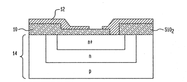
Flgure 1 ls a cross-sectlonal view of an MOS capacitor.
Flgure 2 ls a collector/voltage (C/V) graph lllustratlng
the capacltance of an MOS capacltor havlng
i
~L31~2~
various concentrations of calcium and krypton implanted
into its oxide.
Figures 3a and 3b represent the C/V
characteristics of another example of the invention
prior to annealment and after a final annealing step,
respectively.
Figures 4a and 4b are SIMS cliagrams
illustratiny the distribution of calcium in the
substrate ~efore and ater annealing.
DESCRIPTION OF PREFERRED EMBODIMENTS
In the following description of examples of
the invention, particular reference is made to MOS
structures, where such reference facilitates an
understanding of the invention. It will be
appreciated, however, that the applica~ility of the
invention is not limited to this particular type of
structure. Rather, the field modification that is
achieved with the present invention can be employed in
bipolar devices as well as MOS structures.
2Q Briefly, the basic principle underlying the
present invention is the modification of surface~fields
in semiconductor structures through the placement of
atomic species wi hin a host lattice at a location in
the vicinity of the surface of the host material. More
particularly, the present invention is directed to the
reduction, and more preferably polarity inversion, of
the interfacial field between a dielectric material and
a semiconductor material. In accordance with the
invention, this reduction can be achieved by placing
atoms of elements from groups la, 2a or 3a of the
Periodic Table of Elements in a host dielectric
structure. Since each of these elements has a
relatively small number of valence electrons, it will
1 3 ~
-5-
readily donate electronic density to the structure.
Therefore, by placing atoms of these elements at the
dielectric/semiconductor interface, 21 net reduction of
the positive electric charge can be achieved.
In the case of group la ancl group 3a
elements, however, it has been found that the
particular lattice site for the constituent is critical
to the attainment of the desired results. More
particularly, through theoretical modeling it has been
~ound that placement of the group 1 elements sodium and
potassium at one interstitial site of two linked oxide
crystal cells will result in a negative effective
charge at the surface of the material, but placement of
these same elements at a different interstitial site
will result in a net positive charge. In particular,
placement of an atom at interstitial site 2, which is
the site defined by the coordinates (-1.5258, 0,
4.3288) in two linkPd beta-cristobalite cells, results
in the negative effective charge, but placement at site
1, which is the site having the coordinates (0, 0,
4.3288), results in the positive effective charge.
Thus, to attain a net reduction in the field at the
surface o~ the host material, it is necessary to ensure
that the additive species are located at the proper
lattice siteO This critical dependence upon the
particular site for placement of the atvmic species is
believed to be similarly applicable to group 3
elements.
In contrast, however, the alkaline earth
metals of group 2a provide substantially increased
results relative to ~ite placement. For example,
calcium exhibits a negative effective charge at all
three available interstitial sites, although the
magnitude of the charge is greatest if the calcium is
2 ~
-6-
located at site 2. Experimental results indicate that
strontium and barium also produce negative e~Pective
charges regardless of the particular site location~
Accordingly, the alkaline earth metal~s are the most
preferred species for placement in a dielectric
structure, since net reduction of the surface ~ield is
not dependent upon site placement.
The following examples are provided to
illustrate the behavior of devices resulting from the
implantation of calcium into silicon dioxide
structures.
EXAMPLE I
Layers of oxide were thermally grown on
wafers of 6-9 ohm-cm n-type 100 silicon. The average
thickness of the oxide layers was 770 angstroms + 10
angstroms.
The wafers were divided into three ~roupsO
One group of wafers was implanted with calcium at a
dose of 1 X 10l2 cm ~. A second group of wafers was
implanted with calcium at a dose of l x 10l3 cm 2. A
third group, which functioned as the control group, was
impIanted with krypton at a dosage o~ 1 x 1013 cm 2.
The implant energies were chosen so that the predicted
range (Rp) for each implant would be in the oxide near
the sio2~si interface.
All of the samples were then annealed in the
following sequence: ~
l. 450C for ~0 minutes in a forming gas
comprised of 80% N2 and 20% H2.
2. 1100C for 30 minutes in pure nitrogen.
3. 450C for 40 minutes in the ~orming gas.
MOS capacitors each having a silicon dioxide
dielec~ric 10 interposed between an aluminum gate 12
~31~
and the silicon substrate 14, as shown in Figure 1,
were then constructed with each wa~er. The capacitance
of each capacitor was measured at a frequency o~ 1 MHz
at room temperature and at a biased temperature of
300C.
The result~ of these measursments are
indicated in the capacitance-voltage (C/V) diagram of
Figure 2. As can be seen from the figure, the hiyher
dose calcium implant shifts thP capacitanc2 of the
structure to the right with respect to the lower dose
calcium implant. Basically, the structure behaves as
though an additional fixed negative charge is present
at the dielectric/semiconductor interface.
The reduced capacitance curve resulting from
the 1013 cm 2 krypton implant coincides with the lower
dose calcium curve. This data establishes the fact
that the shift to the right which is found for the
higher dose calcium implant is not due to lattice
damage. Since krypton is more massive than calcium, a
change in capacitance due to damage would have produced
higher results for the krypton than for the equivalent
dose of calcium.
EXAMPLE II
Layers of oxide were grown on silicon wafers.
The wafers were SEH, 100, p-type, 11-18 ohm-cm
substrates and SEH, 100, n-type, 5-9 ohm-cm substrates.
The oxide layers were grown with dry HCl process at
900~C to a thickness of 750 angstroms.
The samples were implanted with calcium at
respective doses of 1012, 1013 and 1014 cm 2~ The
implant energy was chosen at 70 KeV so that ~p was
about 560 angstroms. This depth insured that the
distribution peak of the calcium remained on the oxide
~ 3 ~
side of the silicon dioxide/silicon interface after
annealin~.
MOS capacitors were formed, and the samples
were annealed in the following sequence:
1. 450C for 20 minutes in a mixture of 90%
N2 and 10% H2.
2. 750C for 30 minutes in pure nitrogen.
3. 450~C for 20 minutes in a mixture of 90%
N2 and 10~ H2u
4. 905C for 30 minutes in pure nitrogen.
~. 450C for 20 minutes in a mixture of 90%
N2 and 10% H2.
6. 500C for 20 minutes in a mixture of 90%
N2 and 10% H2.
A control group of samples, which did not
have calcium implanted into the oxide, was annealed in
the same manner. The capacitance-voltage
characteristics of the samples were measured at high
frequency (about 100 KHz) a~ter each anneal step using
a non-destructive mercury probe technique. Between
each anneal, the samples were cleaned in a boiling
H2O2jH2SO4 solution to remove any trace of mercury.
Table I below shows the chan~e in a relevant
parameter o~ the implanted samples, Vmin, as a function
of the Yarious anneals, relative to the control group.
Vmin represents the voltage at which the MOS structure
is inverted and hence corresponds to the threshold
voltage~for a long-channel transistor. Therefore, this
value directly senses the total charge at the structure
at the inversion point. This parameter was chosen
instead of the flat band voltage Vfb for the structure,
since it is easier to identify.
TAB~E I: V . Shifts Associated with Calcium
mlnImplant into si2
1013 Ca~/cm2 implant into 750 A oxide
ANNEALS
#1 #2~#3 + #4) #5 #6
V 5 7 -6.2 -1.0 ~o 4 +0.
V .
~ trol) 0 0 0 0 0
The C/V data for the implanted samples prior
to annealing and after the final anneal are
illustrated, respectively, in Figures 3a and 3b.
: The data contained in Table I indicates a
15 maximum shift in Vmin of 7.0 volts, l.e., (+0.~
6.~)). These shifts are in the positive direction for
each anneal. Thus, the total field charge is becoming
:: less positive ~more negative). Examination of the
practical C/V data illustrates that the maximum error
in the location of Vmin is + 0.15 volts. Thus, the
shifts in Vmin illustrated in Table I are so Iarge,
compared to either the uncertainty in the Vmin value or
the maximum voltage that could:be~attributed to lattice
damage, that the conclusion represented by the data is
that the charge exchange is associated with the calcium
atoms during the~anneallng procedure.
~ 1 3 ~
--10-
The samples implanted with the calcium also
exhibit a low dissipation factor (D~ ~f about 0.03, in
contrast with that of the control sam,ple, which is
about 0.2. This parameter provides a good measure of
the ~uality of the oxide in the MOS capa itor. The
data indicates that the presence of the calcium atoms
does not increase the resistive losses within the
structure which might have been expected on the basis
of damage to the oxide/silicon interface.
To provide optimum contribution to the change
in the interfacial field, the species added to the
dielectric should be located near, but not at, the
interface. If located at the interfacej the positive
ions which result when the additive species give up a
valence electron would cancel the effect which the ~ree:
electrons have on the field. Thus, the implanted ions
: should be located at least two atomic layers away from
the interface, and preferably be in the range of 2-20
atomio layers from the interface, to isolate them from
: 20 the surfaca field... The implant energy should be chosen
so that the implanted species hecomes located within
this range of distances from the inter~ace after final
processing.
~ 3~ 2~
EXAMPLE III
Samples having oxide layers with a thickness
of 750 angstroms were implanted with calcium at a
dosage le~el of 1014 cm 2 and an implant energy of 70
KeV, as in Example II. The distribution of the calcium
was determined using secondary ion mass spectroscopy
(SIMS). The results of this determination are shown in
Figure 4a.
The samples were then annealed in the
ollowing sequence:
1. 500C in 90% N2, 10~ H2 for 40 minutes;
2. 950C in 100~ N2 for 30 minutes;
3. 500C in 90~ N2, 10~ H2 for 40 minutes.
The distribution of the calcium was agin determined,
and the SIMS data is shown in Figure 4b.
~~A comparison of the d~ta shown in Figures 4a
; ~ and 4b reveals that the distribution of the calcium is
substantially unaffected by the annealing process.
Thus, the energy level for the implant process can be
chosen so that Rp falls within the final range of
desired loca~ions for the additive species.
Since atoms of the al~kaline earth metals
strontium and barium are larger~in size than those of
caIcium, they are less mobile than calcium in the
silicon dioxide lattice structure. Accordingly, they
~ 3 ~
-12-
are more stable and contribute even higher electronic
density to the system.
It will be appreciated by those of ordinary
skill in the art that the present invention can be
embodied in other specific forms without departing ~rom
the spirit or essential characteristics thereof. For
example, the placement of the additive atomic species
in the dielectric can be accomplished with an ion
cluster beam (ICB) in place of ion implantation. With
this technique the host lattice would be produced by
means of the beam, and the additive ion introduced by
switching to a different source in the beam generator.
The presently disclosed examples Q~ the
invention are therefore considered in all respects to
be illustrative aod not restrictive. The scope o~ the
invention is indicated by the appended claims rather
than the foregoing description, and all changes that
come within the meaning and range of equivalence
thereof are intended to be embraced therein.