Note: Descriptions are shown in the official language in which they were submitted.
~3~24
NEO 2-037-3
D~T~CIrOR I~ND LOCAL!ZI~R
101~ LOW I~Nl~ C;Y RADIATION hMlSSlONS
13ack~round
Tt~e detection and trentment of cancerous tissue has been the subject
of intense investiGation for mally years. One among the many app{ oaclles to
its detection has concerned the identi~ication of tumor specific antigens.
10 Where these antigens can be identified, radionucleid labeled antibodies have
been employed which tend to collect at tumol sites. When so concentrnted,
sornewh~lt elaborute r adiutioll detection eguiplllent then is employed to
record, for example, by irnagirlg the concelltrations Or the emissive
substances and thus to locate neoplastic tissue. Important advances in this
15 procedure have been evidenced through the use of monoclonal antibodies or
fragments thereof with a variety of rudionucleides. Typical technk3ues for
carrying out imaging of these antibodies have involved, for ~ exam~ple,
tomographic scunning, immunoscintigrayhy and the like. The p~ ticulur
choice of rudionucleid for labeling untibodies is dependent upon its nucloar
20 properties, the physcial half li~e, the detection instrument capabilities, the
pharmncokinetics of the radiolabeled~antibody, and the degree of difficulty
of the labeling procedure. The most widely used of these radionucleides in
nuclear medicine imaging include technetium, 991nTc, iodine 1251, 13 1, and
indium, lllln. Of the above, for locali~ing tumors of tl~e gastro-intestinal
25 tract, the radionucleid 13~1 is used as the marlcel or label in conjunction
with imaging gamm~ camerus and the like which are relativeiy large and
elaborute devices positioned ubove the patient during the imaging process.
In spite of its somewhat extensive utili~ation, 13 1 is not an ideal
rudionucleid for usc in diagnostic medicine. 'rhe high encrgy gamma-plloton
30 emitted from 1311 is poorly detected by the clussic gamlna calneru and lil<e
instrumentation. In addition, thc udministered mark~ emissions deliver a
-i-
. ~
1 3 ~ 2 4
high radiation dose to the patient. Further, the ilnaging definition of these
e~ternal imagillg devices has not been satisfactory for many reasons. As
tumor sites become smaller, the rudionucleid concentrations theredt will
terld to be lost, from an ima~ing standpoint, in the background or blood pool
5 radiation necessarily present in the patient.
Over the recent past, u surgical procedure has been developed
concerning the differentiaeion and removal of sucll neoplastic tissue throu~h
the use of much lower energy garnma eroission levels for example, 1251 t27-
35 kev). While such a radiolabel cannot be ermployed with conventional
10 external imaging or scanning devices because the radiation is Stl ongly
absorbed by the tissue intermediate between the tumor and the surface of
the patient's body, it has been roun~i that when employed with a probe type
detection structure, a hi~hly effective differentiation technique can be
evolved. More particularly, the longer Ilalf life of this type of radiolabel
IS ~oupled with a surgical methodology involving the waiting of appropriate
intervàls froln the time of introduction of ti)e radiolabelled antibody to the
patient to the time of sulgery, cun evolve a highly uccurate dilferentiation
of cnncerous tumor. 'rhis improveel metllo(i of localization, differentiation
and removal of cancerous tumor involves u surgical procedwe wherein the
20 patient suspected of containing neoplastic tissue is admirlistered an
effective arnowlt of an antibody specific l`or neoplastic tissue which is
labeled with a radioactive isotope as above-noted exhibiting photon
emissions of specific energy lcvels. Next, the surgical procedure is delayed
for a tinle interYIll following such adminiselutiorl for permitting the labeled
25 antibody to prererentially concentrate in any neoplastic tissue present in the
patient, as well as to be cleared from normal tissue so as to increase the
rntio of photon emissions from the neoplastic Lissue to the bnckground
photon emissions. T hereaîter, an opera~ive field oiA the patient is surgically
accessed alld tissue within the operative lield to be examined for neoplastic
30 tissue ilas the backgrourld piloton emission COUilt determined. Once thc
background photon elnission count t`or the tissue within thc operative field
has been determined, this hand-held probe is munually positioned within the
perative field adjacent tissue suspected of being neoplastic. I~eadouts then
can be achieved from probe counting for difierentiation. In the abovs
35 regard, reference is made to thc following technical publications:
~3~2~
"CEA-Directed Second-Look Surgery in the
Asymptomatic Patient after Primary
I~esection of Colorectnl Carcillolna", E.W.
Murtin~ Jr., MD, J. P. Minton, MD, PhD,
I.al ry C. Carey, MD. An~
2û2:1 (Sept. 1985 301-12.
Il. "Intraoperutive Probe-Directed Im-
munodetection Vsing a Monoclonal
Antibody", P.J. O'Dwyer, MDl C-M-
Mojzsilc, RN MS, G.II. Ilinkle, RPh, MS, M.
Rousseau, J.Olsen, MD, S.E. Tut~le, MD9
n.F. Barth, PhD, M.O. Thurston, PhD,
D.P. McCabe, MD, W.13. l~alrar, MD, E.W.
Maltin, Jr, MD. Archives of Sur~ery, 121
(Dec., 1986) 1321-1394.
IIL "Intraoperative Radioilnmunodetection Or
Colorec~al Tumols with a lland-~leld
Radiation Detector", D. r. Martin, MD,
C~.l-l. I-linkle9 MS l~Ph, S. Tuttle, MD, J.
Olsen, MD, II. Abdel-Nabi, MD, D.
Ilouchens, PhV, M. Tllul~;ton, PhD, E.W.
Martin, Jr., MD. A Inel ican Journ~l of
Surlrel y, 150:G (Dec., 1985) 672-75.
IV. "Portable G~mmu Plobe ~or n~dioimIllune
~ocalization of ~xperimelltal Colon Tumor
Xenografts", D.J~. Aitken, MD, M.O.
Thurston, PhD, ~.11. Ilinkle, MS I~Ph, D.T.
Martin, MD, D.E. Ilaagensen, Jr., MD,
PhD, D. Moucllens, PhD, S.E. Tuttle, MD,
E.W. Martin, Jr., MD. Journal of Sur~ical
L search, 31;:5 (198~) '180-98g.
3 5
V. ~ adioimmwloguided Sur~ery: I ntra-
operative Use of Monoclonal Antibody 17-
1~ in Colorectal Cullcer". E.W. Martin,
Jr., MD, S.E. Tuttle, MD, M. ~ousseau7
C.l~l. Mojzisik, RN MS, P.J. O'Dwyer~ MD,
G.H. l-linlcle, MS RPh, E.A Miller, R.A
Goodwin, O.A. Oredipe, MA, R.F. 13arthJ
MD, I.O. Olsen, ~MD, D. Ilouchens, PhD,
~ S.D. Jewell, MS, D.M. Bucci, :ns, v. ~ :
~5 ~ Adums, Z. Steplewski, M.O. 'rhulston, PllD,
llybridomu, S Suppl I (1986) 59~-lU8.
Reference further is made to ~ommonly assigned United States P~t.
No. 4,782,840, entitled "Method for Locating, Differentiating, and nemoYing
50 Neoplaslllsl' by Edward W. Martin, Jr.j and Mal lin O. Thurston, issued
November 8, 1988.
~: :
--3--
~. 3 ~
The success of ttlis ~Iighly effective differentiation and localization
technique is predicated upon the availability of a probe-type deteeting
device capable of detectiIlg extremely low amounts of radiHtion necessllrily
developed with the procedure. In tl)is r egard, low energy r adionucleides are
5 used such as 1251 and the distribution of radiolabeled antibody with the
nuclcid is quite sparse so that bacI;gllowld elnissions cun be minimized and
the ratio of ~umol-specific counts received to background counts can be
maximized. Conventionnl radiation detecLion probe-type devices are
ineffective for this purpose. Generally, because a detection device is
10 required for tl~e probes which is capable of performing at room
temperatures, a very fragile or delicatc detection crystal such as cadIniurn
telluride is employed. The probe using such a crystal must be capable of
detecting as little as a single gamma ray emisslon which may, for example,
create electron-hole puirs in the crystul of between ubout 2,000 and 4,000
15 elec~rons. Considering tl~at an ampere generates 6.25 x 10¹⁸ electrons per
second, one may observe that extremely sm~lll currents must be detectable
with such u probc. Ilowevel, the probe system ~lso must be capable of
discriminating such cw r ents fl orn any of Q wide variety of elcctrical
disturbaIlces, for example which may be occasioned from cosmic inputs,
20 room temperature molecular generated noise, and capacitively or
piezoelectrically induced noise developed fi om the mere manipulation of the
probe itself. While being capable of performing under these extremè
criteria, the sarne probe further must be capable of performing under the
requirements of the surgical theater. In this regard, it must be secure from
25 ingress of contaminallts; it must be sterilizable; and it must be rugged
enough to withstand manipulation by the surgeon within the operating room
environ(nent. Further, ~he system with which the probe is employed, must
be c~pable of perceptively apprising the surgeon of when neoplastic tissue is
being appro~ched such thut the device may be employed for the purpose of
30 guiding the surgeoll to tl)e shus of cancer. Additionully, ~or surgical usc,
the probe instrument must be small, so as to be effectively manipulated
through surgicul openings and the like. Sucl~ dirnuni~ive size is not easily
achieved under the above operational criteria. This technique hlls been
described as "rudioimmuno-guided surgery", a surgical approuch developed
35 by l~.W. Martin, Jr., MD, und M.O. 'I'tlurstoIl, PhD
In uddition to the capability of pcrforming under the al)ove-noted
relatively extreme criteria, the prol~e instruIllent culled upon for the inst~lnt
_,~_
~ 31 ~2~
~se preferably should be fabricable employing practical manufac-
turlng techniques. One approach to improving the fabricability
of the probe instruments is described in Canadian Patent
Application 561,451 entitled "Detector and Localizer for Low
Energy Radiation Emissions", filed March 15, 1988. The probe
structurlng disclosed therein is one wherein necessary ground and
bias are applied to opposite sides of the gamma detectiny crystal
utilizing electrodes which are fixed to the crystal face. An
elastomeric retainer is used to struc-tural:Ly retain all the
components together including the crystal, the biasing arrange-
ment, and the like. While successful production has been achieved
with the structure so described, the techni~ue described therein
is one requiring the use of a multi-component cap for the ass-
embly and one wherein deterioration has been noted in the coupl-
ing of the bias and grounding electrodes to the radiation respon-
sive crystals. Further improvements in the structure of the probe
have been deemed necessary both in terms of the integrity of the
association of external components with the gamma radiation
crystal as well as in conjunction with the ease of fabricability
of the probe.
Summary
The present invention is addressed to apparatus for detec-
ting and locating sources of ~mitted radiation and, particularly,
sources of gamma radiation as well as the method of fabricating
such apparatus. Detection is achieved under room temperature
conditions using a crystal such as cadmium telluride and with
respect to very low energy emissions. To achieve the extreme
sensitivity capabilities of the apparatus, an instrumentation
approach has been developed in which the somewhat fragile crystal
is securely retained in isolation from externally induced inci-
dents otherwise creating excessive noise. In this regard, micro-
phonic effects are minimized through employment of a sequence of
materials exhibiting divergent acoustic impedances. Capacitive
or piezoelectric effects occasioned by the most minute of inter-
component movements are controlled to acceptable levels. Com-
pressive retention of the crystal and electrical contacts with
it is employed in conjunction with electrically conductive but
pliable surface supports. The instrument also achieves perfor-
mance while being structured for assembly by practical manufac
turing techniques.
-- 5
~..,
~,".. ..
:~315~2~
A featw~e of the invenLion provides an instrument for detecting and
locating sources of radiation emissions having predetermined energy levels
which includes a housillg huvinE~ a forwal dly di~posed portion. ~ cryst~l
mount is presented wnich is positioned within the housing forwardly disposed
5 por~ion and which is forrne(i of materiul attenuatin~ radiation of the
predetermined energy levels and which has a forwardly disposed, crystal
receiving cavity extending inwardly thereinto from a forwardly disposcd
opening. ~n electric~lly insulative layer is positioned within the CflVity and
a radiation responslve crystal is locuted within the cavity which has a
10 rearwardly disposed surface positioned facing the electric~lly insulative
layer and has a side portion extending to a forw~lldly disposed surfuce. A
biasing arrangemen~ extends within the cavity to provide fl bias contact
adjacent the electrically insulative layer und a first electrically conductive
compliant member which is conformable with anà in contacting acljacency
15 between the crystal rearwardly disposed surface and the bias contact is
provided. A second electrically conductive compliunt me~nber which is
conformable with und in contnctil)g aùjacerlcy witll thf crystal forwardly
disposed surfuce is proviàed arld a glourlding arlurlgelnellt is positioned in
abutting adjacency wit11 the second compliant melnber for electrically
20 grounding the crystal forwardly disposed surface. A resilient retainer is
positioned in tension over the grounding arrangement and the crystal
forw~dly disposed surface for compressively retaining the ground and the
second compliant member against ~he crystal Çorwardly disposed surface and
the rearwardly disposed surface of the crystal against the first compliant
25 member and the bias contact. A forw~rd cover is positioned to enclose the
crystal mount, the crystal, the grounding arrangement, and the resilient
retainels for permitting transmissio~l of the radiation emission of
predetermined energy levels.
Another feature of the invention provides a method of fabricating an
3D instrument for detecting~ and locating sources Or rudiation emission havin~
predetermined energy levels which compl ises the steps of:
providing a housing having a forwurdly-disposed portion;
providing a crysttll Inourlt formed of materiul attcnuating
radiation of the predetermined energy levels and having a forw~ dly
35 disposed crystal receiving cuvity of predeterrnilled depth huving a sidewull
extendin~ inwurdly thereinto rrofn a forwardly-disposed opening;
-G-
~ 3 ~
positioning un electrically insulative layer within the crystal
receiving cavity;
locating un electrical biasing contuct within the c~vity;
positioning a first electrically conducti~e compliant member
witl~ the cavity alld over and in freely-abuttirlg contact with tllt: biasing
contacts;
providing a rndiation response cryst~ aYing a rearwardly
clisposed surface and a side portion extending to a forwardly disposed
surface;
positioning the rearwardly disposed surfacc of the radiation
responsive crystal within the cavity upon the first electricnlly conductive
compliant me~nber;
positioning a second electrically conductive compli{lnt membcr
over thc crystal forwardly-disposed surface;
positioning n flexible grounding contact in freely abutting
contact over the second electrically conductive compliant member;
compressirlg the rlssembly of thc electrical biasing contact, the
first compliarlt member, the crystal, the second cotnpliant member und the
grounding contact by stretching a resilient retainer thereover; and
mounting the colnpressed assemblEIge with the crystal mount
upon the housing forwardly disposed portion.
Other objects of the invention will, in part, be obvious and will, in
part, appear hereinafter.
The inventlon, accordingly, comprises the apparatus und method
possessing the~ construction9 combination of elelnents, steps and
arrangement of parts which ~re exemplified in the following detailed
disclosure. For a fuller understanding of the nature ~nd objects of the
inYention, reference should be had to the following detailed description
taken in connection with the accompunying drawillgs.
Brief Description of ~the Druwin~s
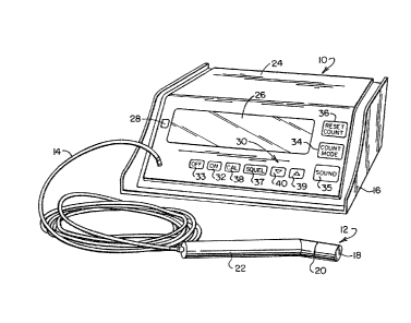
l~ig. 1 is a perspective view of the probe instrument nnd associated
console represcnting the instruillentation of the invention;
Fig. 2 is a side elevational view of the probe instrument shown in Fig.
; ~ 35 I with portions brokerl away to rcve~l internal stlucture;
1 ig. 3 is un exploded view of the forward assembldge o~ the in~trument
of Fig. 2;
--7--
~ 3 ~
Fig ~ is a sectional YieW of the forward portion of the instrulflent
embodiment represented in lliig. 3;
Iiig. 5 is a partial sectional view showing a tooling arranfJement for
providirlg an electrically insulated layer within the caYity of a crystal
S retainer of the instrument of Figs. 2 and 3;
l~ig. G is a perspective view showing the cornponent assemblage of the
instrument of Figrs. 2 anà 3 which is developed during the ~abrication
thereof;
~ ig. 7 is another perspective view of tlle instrurnent of Figs. ~ aIld 3
10 showing a next step in the assembly procedure thereo.;
Fig. 8 is a side view of the probe instrurnent of Fig. 2 showing its
employment with a sterile cover or shefltIl; and
Figs. 9A and 9B combine as labeled to form a block diagr~m of the
functional components of the control system associated with the instrument
15 of the invention.
Detai!ed Description of the Invention
Referring to r2ig. 1, an embodirnent of the probe and supporting
instrumentation of the invention particularly designed for employment in
20 the medical-surgical field is represented generally at 10. This assemblage
includes a hand-manipular probe represented generally at 12 which is
coupled by a triaxial cable 14 to a console 16. The probe 12, which
preferably is retained by ~he surgeon within a disposable polymeric sheath or
cover is maneuvered about the region of sur,rical interest to locate tumerous
25 tissue for resection. When used in conjunction with colonic surgery, for
example, the probe 12 is maneuvered through a surgical opening in the body
cavity and essentially brought into contact with orgQns under study by the
surgeon. When employed in a radioimmuno~ruided mode, a loudspeal:er or
annunciator withln the console 16 muy be activated to provide a "siren"
30 form of output which apprises tlle surL~eon that the probe 12 is at a site ofcancer. Thus, it is necessary th~t the device 12 be of convellient length and
comfortable to frrasp. The probe 12 is seen to include a radiution
acceptance surface or window 18 located ~t the tip of an angularly oriented
portion thereof 20. Portlon 20 extends from a I-and~rippable portion 22 at
35 an nngle of about 30 to fflcilitate its manueverability ubout the back or
hidden side of or~runs and, preferably, is coated with a low-friction surface
material such ns 'I'l~l~LON ~polytetrafluol oethylene) to enhaIlce noise
~3~24
avoidance otherwise occasioned by the rubbing of surf~ce 18 over tissue and
the like during surgery.
Bec~luse the asselnblage 10 is used in a surgical theater, the console IG
also is readily clea1led, haYing a smooth, one-piece touch sensitiYe polymeric
5 surface 24 surmounting a r elatively lalge LCD readout or displuy 26, a dual
colored LED readout 28 and n sequence of finger-actunted switches. Thcse
switches or keyboard, as represented gener~lly ~t 30 permit the
Inicroprocessor driven conso~e 1~; to c~ ry out an instructive or "user
friendly" dialogue with the practitioner. Iior purposes of safety, th0 device
10 is powered by a rechargeuble battery.
In addition to conventionul on and off switches shown, respectively, at
32 arld 33, the switches provided on the console 16 ;nclude a count mode
switch 3~1, u sound switch 35, a reset count switch 3G~ a squelch function
switch 3r, a calibrution function switcll 38, and up and down incrementing
15 switches for adjustment within certain of the switch generated modes as
shown, respectively, ut 39 and ~0.
The probe 12 must be capable of performing essentiully at room
temperature. l'hus, the device employs a c~dmium telluride crystul and,
because of the preferred low energy levels of radiution which it is calIed
20 upon to detect, must be capable of operatively reacting to low energy
gamma ray interactions. The interaction of gamma rays with such crystals
is primarily through three processes, namely the photo-electric effect,
Compton scattering, and pair production. In the photo-electric effect, a
photon of energy, S~v, interucts with ~n atom as a whole. Its energy is
25 completely transferred to an electron, usually in the innermost shell. The
electron Is ejected witll n kinetic energy: el~jn = hv - Eb~ where Eb is the
binding energy of the orbital electron, h is Planck1s constant, and v is the
frequency associated with the wave nature of the gamma r~diation. Such
electrons undergo many collisions until this energy is shared with some
30 thousunds of other electrons. E.ach of these clectrons leaves behi1ld a
positively churh~ed regiorl called in the literature u "hole". At the cnergies
of 1251 Compton scattering is of minor ilnportance. Pair production refers
to the reaction of an electron and ~ photon to the gamma ray. Since this
process requires more than 1.0 Mev it does not occur in the present
35 application. In Compton scattering, the prirnary photon may interact with
any one of the orbitul electrons. The electrons are considcred esserltially as
free electrons undcr the condition that tl1e prin1uly photol) energy is large
_~_
13~2~
compured with the electron binding ener~y. 1`he interaction may be
analyzed as the elastic collision between the primary photon und the
electrom Energy is si~ared between the recoil electron and ths secondury
photon. This secondury photon travels in a directiorl differellt froln th~t of
5 the primary photon, and is referred to us the scattered photon.
Tllus, as an incorning gamma ray is absorbed by the crystal, it
transfers some or all of its energy to electrons, which as ch~rged particles
pass through the semiconductor producing electron-hole pairs and,
therefore, t~e capabili~y Or charge-transfer wiLhin the crystal medium.
When a charge particle produces electron-hole pairs in the semi-
conductor, the electric field causes these charge carriers to move toward
and accumulute at the appropriate electrodes. As these charges move
toward or D~ e collected at the electrodes, they induce a churge or electrical
pulse signal in the circuit external to the detector. It is then necessary to
15 pre-amplify these signals and feed them to the electronics of the control
w~it or console 16.
For effective performance, the probe 12 rnust be capable of
gener~ting and discerning signuls representin~ gumma ray strikes which are
of extremely low energy. In this regald, a galnma ray interaction with the
20 cadmium telluride crystal may produce two to four tilousand electrons. It
beinL~ recognized that 6.25 x 10¹⁸ electrons per second represents one
ampere of current, the relative sensitivity of the inst~nt device will become
apparent. As a consequence, the mechunical structuring of the mounting
arJangement for the cryst~l witliin the probe 12 is of critical importance as
25 is the technique for detecting and treating these significantly small charges representing gamma ray interactions.
Looking ~o Fig. 2, a more detailed representation of the probe device
12 is revealed. The angular orientation of the fiont portion 20 is shown
having the noted 30 cant with respect to the central axis of the hand
30 gripped portion 22. Device 12 is small huving an overall len~th of about
1~ cm and portion 22 having ~a len~tll of about 12.7 cm. 'rhe overull
diameter of the cylindrical structure 12 is about 1.9 em. Experience to the
present, utili~ing low ener~y radiolabeling and achieving very high
sensitivity on the part of the probe, for mar-y applications hus removed the
35 need for supplementary forwurd collimation. The hand grip portion 22
carrics a prcamplifier on an elongate Cil'CUit board as r eprcsented in ~ener~l
at ~}4. I~eperlding~ upon the energies of radiatioll encountercd, the probe 12
-10-
~31~424
housing is formed of an electrically conductive and thus shiel-
ding material which functions to attenuate radiation.
Cable 14 supplies power to the preamplifier of the probe,
as well as bias and ground to the crystal and functions to trans~
mit the preamplifier treated output signals. Cable 14 includes
silver cladding components 46 and 48 which are mutually insulated
and spaced by a polytetrafluoroethylene cover *(TEFLON) 50 which
is somewhat loose to permit flexure. The innermost leads, formed
of TEFLON insulated silver, of the arrangement at respective
lines 52 and 54 carry the output signals from the preamplifier
44 and a bias signal, for example 30 volts, for application to
the rear face of the crystal within the device 12. Clad 46 car-
ries a 12 volt power supply for the preamplifier circuit, while
outer clad 48 carries ground for the system. An outer silicon
rubber cover then is provided at 56~
Looking to Fig. 3, an exploded detail of the nose or forward
portion 20 of probe 12 is provided. This portion 20 retains a
radiation responsive crystal 114, formed preferably of cadmium
telluride, in a light-tight and mechanically secure orientation
while maintaining necessary ground and bias conditions upon it.
Generally, such crystals as at 114 will have a rigidity or phy-
sical consistency somewhat similar to chalk and are formed having
very light gold coatings on their surfaces. Thus, the mounting
of such delicate crystals and their operation within a probe
instrument as at 12 requires a highly refined design architec-
ture. However, it is also important that the structure of the
probe 12 be such as to permit its fabrication in a reasonably
practical manner.
Fig. 3 shows the hand-graspable portion as at 22 extending
to a supporting tubular portion 70. The forwardly disposed
tubular region of portion 70 including its cylinder connector
surface 72 are configured havin~ an internal diameter defining
a chamber 74. Chamber 74 receives a generally cylindrically
shaped slug or crystal mount 76 along with a conductive epoxy
retainer layer 146 (see Fig. 4) which retains the slug 76 in
position.
*Trade mark
-- 11 --
:~3~ 5~2~
Slug or crystal mount 76 is formed of a suitable radiation
attenuating material such as lead and is of a generally cylin-
drical configuration. In this regard, the rearwardly disposed
cylindrical surface thereof 78 is configured for the noted
slidable mounting within chamber 74 of the housing rearward
portion 22. Extending centrally through slug 76 i.s an access
opening gO passing therethrough to a forwardly-disposed cylin-
drical recess represented
- lla -
,. ,,.~.
~3~2~
generally at 82. Opening 80 functioIls to carry an insulated lead 84. Lead
84 functions as a bias-signal transInission wire leadin~ to the physically
adjacent preamplificution stage 4~ within the hand-graspable portion of the
instrument at 22. Ti~e cylindrical surface 78 of slug 76 is seen to terminate
S at a cylindricaI collar region thereof 8G which is configw~ed havitlg anunI)uIar retainer groove 88 forIned tllerein and which further incorporates a
bore 90 extending in gas flow commuIlication with the centrally disposed
opening 80. Bore ~0 serves to equalize gas pressure between the handle or
hand graspable portion 22 of the instrumerlt and the forwardly disposed
components. The bore fur~her functioIls to receive a tool for facilitating
removal of the slug or crystal mount 7C und its associated assemblage of
components for maintenance purposes and the liIse.
Within recess 82 there is formed, in situ an electrically insulative
luyer 92 whicil additionally functions as a cushioniIlg mount for the cadmium
telluride crystal 114 of the assemblngæ Formed from a silicon rubber/ the
layer 92 is structured such that its externul surface defines the walls of a
crystal receiving cavity represented generally at 104, the side surfaces of
which are depicted at 94 and the bottom surface of whicll is sho~n at 96.
Additionally forrned with this materiaI is an annular depression 98 which is
2U configured eo receive a correspondingly configured bias contact member 100
formed at the terlninus of insulated lead ~4. Contact 100, for example, may
be formed of an electrically conductive copper foil adhesively retained upon
the leads withiil insuklted Icad 84. With the provision of the depression 98,
the bias contact member lOû may be flush Inounted along the bottom
surface of the insulative layer whicII as noted may also serve to provide a
cushioning effect. The sides 94 of the layer 92 defined cavity 104 are of a
length for fully receiving the corresponding sides 97 of the crystal 114 to be
rnounted therein. Note that the radiation attenuating materiul of the
crysk~l mount 76 at sides 102 forming recess 82 is coextensive witl~ the side
9~ of the cavity 104. This portion of the retainer 7G collar or shoulder 86
functions to block radiation otherwise incident on the sides o the crystal
when it is positioned~ within the assembluge.
The widthwise extent oÇ tlle cavity 104 across the inwardly disposed
surfaces of sides 9~1 thereof is slightly greater than the corresponding
3S widthwise extent of crystal 114. /~ spacing or gap 95 (Fig. 4) thus is formed
between cavity sides 94 und the sidc surl`uce 97 Or crystal ~ or
example, for a cylindrically shnped cIystul as depicted, the cavity 104 is
-12
~3~2~
cylindrically shaped having a slightly greater outer diameter
then the crystal. This small gap 95, for example 0.005 inch,
serves to prevent noise phenomena resulting from any contact
occurring between the side 97 of the crystal and the cavity 104
sides 94. Accordingly, gap 95 is formed having a width effective
to avoid electrical noise phenomena which otherwise may be
generated or occur as a consequence of contact between crystal
side 97 and cavity side surface 94.
Cavity 104 including side surfaces 94, bottom 96, and
depression 98, preferably is formed with a tooling arrangement
wherein its shape and dimensions are customized to the cor-
responding shape and dimension of the crystal assemblage to be
inserted therein, taking into account the formation of gap 95.
Looking to Fig. 5, a tooling arrangement for so customizing the
cavity 104 by the process of molding layer 92 is revealed. The
material used for layer 92 may, for example, be a silicon rubber
identified as "Two-Part *RTV" rubber marketed by Chembar, Inc.
Groveport, Ohio 43125. This material is prepared by combining an
HF RTV silastic material with a catalyst in accordance with a
predetermined ratio. The material is poured within recess 82 of
the crystal retainer 76 and a -tool 106 which is comprised of a
rectangular aligning bar 108, a male crystal mold 110, and a
centrally-disposed aligning bar or rod 111 is insarted into the
deposition. Note that rod 111 protrudes downwardly into opening
80 and that the mold 110 incorporates a cylindrical protrusion
113 functioning to form the earlier-described depression 98. In
general, the silastic material is located about recess 82, where-
upon the tool 106 is inserted for an interval sufficient to per-
mit curing. The tool 106 then is withdrawn and the resultant
silastic layer 92 is one which receives the crystal and related
components to be positioned therewithin with the spacing deriving
gap 95. While providing electrical insulation, layer 92 also
serves to contribute a cushioning function.
Returning to Fig. 3, upon positioning the bias contact
member 100 as coupled with lead 84 within the depression 98 of
layer surface 96, an annular or disk shaped electrically con-
ductive compliant member 112 is positioned over the biasing
contact 100 in ~reely-abuttable fashion. The compliant member 112
*Trade mark 13 -
~,~
,1
~315gL2~
preferably is formed of a non-woven TEFLON cloth (stretched,
highly crystalline, unsintered polytetrafluoroethylene) marketed
under the trade designation ''CORETEX'I having a thickness, for
example, of about 0.020 in. and being filled with carbon par-
ticles to establish the requisite
- 13a -
~,
.
~L3~2~
electricul condus~tivity. Component 112 not only functions to provide an
intimate contact with biasing component 100, but, importnntly, serves to
estublish n corresponding electrical contact with the radiation responsive
crystul 114. The reurwardly disposed face 116 of crystal 114 I`reely abuts
against the conforming surface of component 112 to develop an intimate and
surface-conforrning electrical contact. Additionally, the component 112
serves t~le important function of cushioning the clelicate crystal 114.
Ground potentinl is applied to the opposite or forwardly-disposed face
118 of crystal 114 Tllis is carried out by positioning another conductive and
compliant member 12U which may be configured identically as member 112,
(carbon filled non-woven TEI~LON) in freely abuttable fushion over surface
118. I~s before~ the component 12U serves to provide a freely-nbuttillg
electrical contact through a conformin~ intimacy with surîace 118. To
establish a ground potential, four thin plantinum wires 122-125 are provided
which are swaged within respective grooves 128-131 formed within surface
102 of slug 76 as seen in Fig. 6. The wires 122-125 then are bent over as
shown in I~ig. 6 to contuct the forwardly-disposcd sulface of cornpliant
member 120. This sub-assembly is secured by a small dislc 13~ of
transparent tape.
The small, tllin platinum wires 122-125 establish an appropriate ground
condition at the forward face 118 of crystal 114 through member 120 while
imposing only a very minimal potential blocl~age~ of any impinging radiatlon.
To enhance and stabiliz~ the electrical contact both from wires 122-125 and
the biasing eontact melnbcr 100, the asscmblage of disk 134, compliant dislc
120, cryst;~l 114 compliant disk 112, biasing contact 100, ~nd layer 92 are
r etained in a compressive, physically Ot' dynamically stable state by a
resilient retainer 136 which is positioned in tension over the noted assembly
nnd retained in such tension by a conventional elastic O-ring 13~ which
engages the retniner 136 within groove 88 of crystal retainer or slug 76.
Looking additionally to ~ig. 7, the reLaincr 136 is represented as a
resilient web which may be forrned of nylon or the like. The web is
positioncd over the noted assemblage of components and drawn downwardly
over them as well as over the outer surface 1û2 oî retainer 7G to be retained
in such tension by tlle O-ring 138. A simple cup-sllaped jig may be employed
for this purpose. The resultant nssemblng~e has been found to both effect
stabilization of the electricul contacts for biasillg nnd ~roundirlg purposes,
--1~1-- ,
~3~2~
and to retnin all components in adjucency with crystal 114 in a desir~bly
static~lly stable state to Elvoid the ~eneration of motion induced noise.
neturning to I~ig. 3, a forwurd cover 140 is positioned over the aboYe-
described assemblage us it is installed within llousing cilalnber 74. 13ecause
5 of the extension of thc radiation shielding material, such as lead, of retainer
76 about the sides of crystal 114 by virtue of the side poltiorls 102, the
forward cover 140 may be maàe entirely and unitarily of a convenient
r~di~tion transmissive mnteri~l such as nluminum. This avoids the
formation of jwlctions at the periphery of window component 18 which may
10 be prone to break down and consequently permit ingress of fluids and the
like fro(n the surgical tlleater. Because the coYer 14V functions as an
electrical shield, the interior side surfaces thereof are made electr.cally
conductive by the deposition thereon of a thin layer of gold as at 14~.
Finally, the external surface of the cover 140 preferably is coated with a
15 polyrneric low sllrface friction coating 14~. This layer 144 may, for
example, be provided as Teflon. The coating functions to aid in avoiding
friction generated noise occasioned by the movement of the device over
tissue and the implements typically encountered in a surgic~l thetlter.
Looking to I~ig. 4, the final assembly of the instrument portion 20 is
20 revealed in sectional detail. Note, that the retainer or slu~ 76 is adhesively
coupled to suppor ting tubular portion 70 with a layer of electrically
conductive epoxy cement 146, while the forward cover 1~0 additionally is
retained over portion 72 of the housing by a conductive epoxy cement layer
148 Note in Fig. 4 that the assemblage of tubulul portion 70, crystal 114,
25 and the components associated therewith are so oriented upon final
assembly that a dead space 150 is created between the forwardly-disposed
surface 118 of cryst~l 114, as well as the associated cushioning, retainer,
tlnd electrical contact components, ~nd the window portion 18 of cover 140
This dead air space provides an enhancement of acoustic isolation of the
30 crystul 114.
As represented at circuit 4~ in 1; ig. 2, in ordel to carry out the
tre~tment o~ the very ~uint charges which are evolved due to gam rnu
interaction with crystal 114, it is important that the preamplificution
function take place as close as possible to the situs of the interuction. In
35 view of the operationul need in surgely for the 30 cant of the central axis
of the fcrwurd portion 20 with respcct to the corresponding axis of the
rearwal d SuppOI t pos tion 22 ol the probe 1'~, the small length of
-15-
1 3 ~
transmission wire 84 is required. Because extremely small churges of
current ure involved in the range of 300-600 atto-coulombs9 d
preamplification stuge which performs to achieve a very hi~h gain is called
upon but one whicl1 performs with IQW noise generation. In effect, the
5 preamplification staL~e of the instant appalatus is one achieYing a voltage
amplifi~ation, for example on the order of about 25,000.
Crystal 114 is maintuined in a carefully electrically shielded,
acoustical1y dead and light-tight enYirOnlnent. Aluminum cover 140 pcrmits
entry of very low level emissions of gamrna radiation. Thus, the full
10 forward face 118 of crystal 114 is exposed to radiation. Even though the
window 18 portion of the cover 140 is relatively broad in extent, the
capability of the instrument 12 to differentiate the interface between tissue
carrying radiolabell(3d antibodies und the like and those not earrying these
labels is quite accurate to the extent that colli mation to ach~eve close
15 diffel entiation typically is not required.
A technique which botl1 sirnpli ties cleaning the instrument and
maintaining its sterile conclition involves the use of a disposable plastic
cover which fits over the probe device 12 and which i~ ~ormecl of a
polymeric mllterial which is readi!y produced in n sterile state. l`hus, prior
20 to an operation, the surgical personnel will slide the probe within the coveror sheath. The addition of the polymeric surface uids in the control of
vibration induced noise as well as representing an ideal technigue for
maintaining the reguisite sterile condition for the device. Lookin~ to Fig 8,
the instrument 12 is shown in dashed line fashion with a polymeric cover
25 154. Cover 15~ includes a nose portion 15G forrned of a tOUgi1 plastic~hnvinga thickness, for example, of 0.020 inch. This will protect the cover i54
from tearing or the like when used in the rigorous activities of surgery.
From the nose portion 156 the sheath may extend rearwardly a sufficient
length to cover the signal transmission components as at 14 for u sufficient
30 distance to assure sterile integrity.
Referring to Fi~s. 9A and 9B, a block diagrammatic representation of
the instrumentation circuitry is revenled. In Fig. 9A, the cadmium telluride
crystal 114 is sho~n having one face coupled to ground through line 157,
while the opposite, biased face thereof is coupled via lines 158 and 159 to a
35 bias filter represented at block 16U. The input to the filter 160 is
rcpresented at line 161 as bcin~ npplicd througll the triaxinl cable as
described earliel ut 14 and repres(!llted by thut numelal herein. I.ine 158
-16-
~31~i~2~
corresponds with the earlier-described line 52 in Fig. 2. This bias emanates
from a power supply shown at bloclc 1~;2 in F ig. 913 and represented at line
1(~3.
Line 158 from the crystal 114 is shown extending to an integrlltor
stage 1~4 of the preamplifier 44. The integrated valuation of detected
radiation disturbance then is shown directed as represented by line 1~5 to a
driver-amplification networlc shown at block 1~6. A 12v power supply is
provided from the power suE~ply 162 (Fig. ~B) as represented at line 167
which, as shown in Fig. 9A~ is directed to a probe current networlc
represented by block 168. Under microcomputer cos~.trol as represented by
line 169, the network 168 develops signals, for example, determining
whether the probe instrument 12 has been properly connected to the console
16. Delivery of the 12v power supply for the preamplifier stage 44 is
represented at line 170 ~s extending to the driver amplifier from cable 14
via line 171. Line 171 corresponds with the clad 4G described in conjunction
with cable 14 in Fig. 2.
Ground to the instrument 12 also is developed from the power supply
block 162 as represented at line 172 showll in liig. 9A ns extending to cable
14 and via line 173 to the instrumerlt preamplification cornponents 44. Line
173 corresponds with tile earlier-described clad at 48 in Fig. 2.
The output of the preamplification circuit 44 is reprcsented at line 174
extending through the cable representation 14 corresponding with t!le
earlier-describ~d line 5~ in Fig. 2. Line 174 extends from the cable 14 ~s
line 175 to thc input of a normali:~ing amplifier represented at block 176.
The network represented by block 176 functions to amplify or atterlurlte, i.e.
scale the noise characteristic of any given instrument 12 and normalize the
value thereof or render it consistent for later comparison stages. Generally,
for example, the 27 Icev energy level g~mma r~y ~enerated pulses in the
system will be about five times higher than noise levels. Normalizillg
amplifier networlc 176 will establish those noise levels at some
predetermined level, for example, 200 mUlivolts and the resultallt
proportionRl valid gamma r elated pulses will become about one volt high for
purposes of ensuing comparison functions. ~t may be observed that the
amplifier network at block 171i is shown controlled from a digital-to-nnalog
converter network represented at blocl; 177 via line 178. Network l771 in
turn, is controlled ~rorn line 17~ extcndillg, ns shown in Fig. 911, to block 180
represcnting a rnicrocomputer nctworlc. The norlnali~ed output developed
-17
13~2~
from nctworlc 176 is presented along lines 181 and 182 to a noise aYerager
circuit as repres~nted at bloclc 183. This networlc 183 deterrnines an
averuge amplitude value for the noise of u given system with a given
instrument 12 and provides a correspondinbJ signul as represented at line 184
5 (noise amp) which is employed as above-described as information used by the
microcomputel 180. This information, in addition to being employed with
the normali:~ing ampli~ier network represented at block 176 may be used to
devclop a low window Yuluation for the comparisOn function.
Line 182 also extends via line 186 to a pulse acquire network
10 represented at block 188. This network fwlctions, when nctivated by the
microcomputer represented at block 180, to acquire the vnlue of the highest
puLse amplitude witnessed at line 186. Periodically, this information then is
translnitted to the microcomputer at bloclc 180 as represented by line 190.
Representing a form of peak detector, tl~e networlc is sometimes referred to
IS as a "snapshot circuit". Also produced frorn line 182, as at line 192 and
bloclc 194 is a buffer arnplifier which will provide at line 196 an output
represcnting received pulses which may be made available at the rearward
portion of console IG for conventional rucliation evaluation purposes.
Line 181 extends, as shown in Fig. 9B at line 198, to one input of an
20 upper window compurator represented at block 200 and a lower window
comparator illustrated at block 202. The threshold level for comparative
purposes employed by the network at block 202 is shown asserted from line
204 and, preferubly, is developed by the logic of microcomputer network 180
at a level just above the noise amplitude signals generated from line 18~1
25 Of course, manual setting of such windows can be carried out. In similar
fashion, the upper window of acceptance Çor valid gamma r~y interaction is
established frorn a correspondilig l;ne 206. This threshold setting may be
made îrorn the in~ormation talcen from pulse acquire network 188.
l~eturning to Fig. 9A, the upper window and lower window threshold
30 selections are made under the conLrol of the microcolnputer network at
block 180 as controlled from the digital-to-amllog networic shown at~ block
177. It is the characteristic of such networks as ~t block 17'l to provide an
output which is comprised, for example, of 256 steps of varying amplitude.
The percentage of inCrementatiOrl from step-to-step will vary somewhat
35 over the range of voltage values provided. Accordingly, the outputs from
this con~ersion network at bloclc 177, as ~It Ihles 208 and 210 are directed to
squarer networks shown, respectively, at blocl;s 212 an~l 21~}. These
-18-
~3~24
networks function to square the current outputs at lines 208 and 210 und
thus achieve a uniform percentage incrementation of the threshold defining
outputs at lines 204 and 206.
Returning to Fig. 9B, the outputs of the comparator networks shown ut
blocks 200 and 202 represent candidate pulses which may be ubove or below
the ~iven tllresholds and are identified as being prescnt~d as a "UW pulse"
and an "LW pulse" along respective lines 216 and 218. Thcse lincs are shown
directed to a real tilne pulse discrirninator network represented at block 220
which carries out Boolean logic to determine the presence or absence of
valid pulses. Valid pulses are in~roduced to the microcomputer network 180
as represented by line 222.
The microcomputer represented at block 180 performs under a number
of operational modes to provde both audio arld visual outputs to aid the
surgeon in locatlng and dif~erentiating tumorous tissue. In the former
regard, as represented at line 224 and block 226, a volume control function
may be asserted with amplitude variations controlled from a solid-stnte
form of potentiometer us represented ut line 228 und block 230. Further, a
"siren" type of frequency variation m~y be nsserted as represented at line
232 to an audio amplificution circuit represented at bloclc 234 for driving a
spealcer as represented at 236 anà line 238. With the noted siren
arrangment, the frequency output from speaker 236 illcreases as the
instrument 12 is moved closer to the situs oî concentrated radiation. Of
- course, conventional clicks and beeps can be provided at the option of the
operator.
The microcomputer network 180, as represented by arrow 240 and
block 242 also addresses an input-output network whichp as represented at
arrow 244, functions to provide a pulse count output of varying types ~s well
as outputs represented volume levels, pulse height, noise le~els and battery
statùs. Visual readout is represented in Fig. 9B as ~ block with the same
display 26 numeration as described in conjunction with Fig. 1. Similarly1 the
input-output function representcd at block 242 provides appropriate
seanning of the keyboard or switches described in conjunction with I~ig. I at
30 and represented by the same numeratioll in l~ig. ~B. During the counting
operation, the microcomputer networ~ 180 functions to control a li~ht
emitting diode drive network represented by bloclc 246 from line 24B. The
drivc network represented At block 246 is shown providing an input, ns
represented by line 250 to the duul LED display as dcscribcd at 28 in l~ig. 1
~3~ ~2~
and represcnted in block forrn wlth the same numerution. This readout
provides a red light when a gamma ray is detected und a green light during
the counting procedure in general. A serial output port of conventional
variety also is provided on the console 16, such ports being represented at
S block 252 being addressed froln the microcomputer at block 180 from line
254 und having output und input components represented by arrow 256. A
real time clock-calenclar havillg a non-volatile memory also rnay be provided
in conjunction witll the functions of the microcomputer network 180 us
represented by block 258 and arrow 260. Furtller, the microcomputer may
be ernployed to monitor ~he performallce of the power supply represented at
block 162. This is shown being carried out by the interuction of the
rnicrocomputer network with Q multiplexer represented at block 21i2 and
having an associatlon represented by arrows 264 and 26(;. It may be
observed that the power supply also provides a -~5v source for the logic leYel
components of the circuit as represented by line 268; a -5v source at line
270, us well as a -9v reference at line 272 fol display 26 drive und, finally,a
2.5v reference as represented at line 274 to provide reference input to the
analog circuitry described later herein.
I~eturlling to Fig. 9A, the microcomputer network us represented ~t
block 180 also provides an input to the digital-to-analog conversion network
represented at block 177 which corresponds with the inst~ntaneous pulse
rate and this information is conveyed to a pulse rate amplifier network
represented at block 27B via line 278. The resultant output as represented
at line 280 may be provided, for example~ at the rear of the conso}e 16.
This circuit represented at block 276 also may be employed to generate a
calibrating pulse for testing the downstream components of the system.
Thus, the microcomputer applies a predetermined pulse level through the
digital-to-anulog conversion network at block 177 for presentation to the
amplifier network represented at block 276. The resultant output at line
282 is selectively switched as represented by block 284 to define pulse width
from the microcomputer input at line 286 to the culibratin~ pulse at line
288.
Since certain changes may be made in lhe above-described system and
apparatus and method without departing fiom the scope of the invention
herein involved, it is intended thut all Inatter contained in the description
thereof or showll in the accompanying drawings shall be interpreted as
illustrative and not in a limitin" sense.
-20-