Note: Descriptions are shown in the official language in which they were submitted.
13~5548 FJ-6479
PROCESS FOR MANUFACTURING A~ OPTICAL ~ECORDING MEDIUM
BACKGROUND OF THE INVENTION
1. Field of the Invention
The present invention relates to a process for
manufacturing an optical recording medium which optically
records digital information, including a write-once
optical recording medium on which a user can write
information only once and an erasable optical recording
medium on which information can be repeatedly written
and erased.
2. Description of the Related Art
The present inventors have already disclosed
optical recording mediums using a recording layer which
takes two stable crystalline states exhibiting different
optical characteristics transformed by an irradiation of
light pulses having different powers and irradiation
times in Japanese Unexamined Patent Publication (JUPP)
(Kokai~ No. 61-134944 published on June 23, 1986; JUPP
~o. 61-168145 published on July 29, 1986; and, JUPP
No. 61-168144 published on July 29, 1986, among others.
These recording mediums are provided with a recording
layer having a uniform chemical composition in the
direction of the layer thickness and are manufactured by
depositing a layer having the chemical composition on a
substrate while heating the substrate or by depositing
such a layer followed by scanning tracks of the deposited
layer with a laser beam, so that the deposited layer, or
only the tracks of the deposited layer, are crystallized.
However, these processes are disadvantageous
in that they require a long time for heating and cooling
a substrate or for scanning a laser beam, and further,
require a substrate having a high heat-resisting feature.
Moreover, in the above processes, the reflectivities of
a recording layer can not be altered over a wide range
by selecting a thickness of the recording layer, since
the recording layer has a uniform chemical composition.
1315548
2 --
The inventors developed another process for
manufacturing such an optical recording medium, which
comprises depositing a plurality of layers followed by
heating the layers to form a recording layer (see Japanese
Unexamined Patent Publication (Kokai) No. 62-20,154,
published on January 28, 1987). However, this process also
requires a long manufacturing time, and has a disadvantage
in that the characteristics of the resultant recording
medium are inferior.
SUMMARY OF THE INVENTION
To solve the above mentioned problems, according
to one embodiment of the present invention, a recording
layer on a substrate is formed by successively depositing
a combination of a plurality of layers having a lower
crystallizing temperature, i.e., a layer of an element or
a layer of an intermetallic compound, to obtain a required
chemical composition as an average chemical composition
thereof, and heating the substrate during deposition of the
plurality of layers.
Thus, in accordance with an embodiment of the
present invention there is provided a process for
manufacturing an optical recording medium including a
recording layer of an alloy, the recording layer of an
alloy being crystalline and capable of taking two different
crystalline states having different light reflectivities.
The process comprising the steps of: preparing a
substrate; and successively depositing a plurality of
layers on the substrate while heating the substrate at a
temperature lower than the thermal deformation temperature
of the substrate, at least one of the successively
131~5~8
- 2a -
deposited layers consisting essentially of an element
composing the alloy or a chemical compound of two or more
elements composing the alloy, the successively deposited
layers having an average chemical composition of the alloy.
The successively deposited layers have an average chemical
composition represented by the general formula selected
from the group consisting of:
l) (In1xSbx)1yMy wherein 0.4 < x < 0.8,
0 < y < 0.2, and M is one or more of the group consisting
of Al, Si, P, S, Zn, Ga, Ge, As, Se, Ag, Cd, Sn, Bi, Te, Tl
and Pb;
2) (In1xAsx)1 ~y wherein 0.2 < x < l.0,
0 < y S 0.2, and M is one or more of the group consisting
of Al, Si, P, S, Zn, Ge, Bi, Se, Ag, Cd, Sn, Sb, Te, Tl and
Pb;
3) (In1xBix)1yM wherein 0.2 < x < 0.7,
0 < y < 0.2, and M is one or more of the group consisting
of Al, Si, P, S, Zn, Ga, Ge, As, Se, Ag, Cd, Sn, Sb, Te, Tl
and Pb;
4) (Ga1xSbx)1yMy wherein 0.4 < x < 0.9,
0 < y < 0.2, and M is one or more of the group consisting
of Al, Si, P, S, Zn, Ge, As, Se, Ag, Cd, Sn, Tl, Te, Bi and
Pb;
5) (Ga1xBix)1yMy wherein 0.4 < x < 0.7,
0 < y < 0.2, and M is one or more of the group consisting
of Al, Si, P, S, Zn, Ge, As, Se, Ag, Cd, In, Sn, Sb, Te, Tl
and Pb; and
6) (Tl1XBix)1yMy wherein 0.5 < x < 0.8,
0 < y < 0.2, and M is one or more of the group consisting
of Al, Si, P, S, Zn, Ga, Ge, As, Se, Ag, Cd, In, Sn, Sb, Te
/7~
~ ~i'J.~
131~5~8
- 2b -
and Pb.
In accordance with another embodiment of the
present invention there is provided a process for
manufacturing an optical recording medium, comprising the
steps of: preparing a substrate; first depositing a layer
of an element Sb on the substrate while heating the
substrate at a temperature lower than thermal deformation
temperature of the substrate; and then depositing a layer
of an intermetallic compound of InSb on the layer of Sb, an
average chemical composition of the layers of Sb and InSb
being 50% to 70~ by atom ratio of Sb and the remainder of
In, while heating the substrate at the temperature.
In accordance with yet another embodiment of the
present invention there is provided a process for
manufacturing an optical recording medium, comprising the
steps of: preparing a substrate; first depositing a layer
of an intermetallic compound of InSb on the substrate while
heating the substrate at a temperature lower than a thermal
deformation temperature of the substrate; and t h e n
depositing a layer of an element of Sb on the layer of
: InSb, an average chemical composition of the layers of InSb
and Sb being 50% to 70% by atom ratio of sb and the
remainder of In, while heating the substrate at the
temperature.
BRIEF DESCRIPTION OF THE DRAWINGS
Figure 1 is a schematical view of a system for
evaporating an alloy layer;
~C
1. .
1 3 1 ~
Fig. 2 is a sectional view of an optical recording
medium according to the present invention;
Fig. 3 shows a relationship between a CN ratio
(carrier to noise ratio) of a recording medium and a
recording power;
Fig. 4 shows a relationship between a CN ratio of a
recording medium and a number of repetitions of writing
and erasing;
Fig. 5 shows a relationship between a C~ ratio of a
recording medium and a recording power;
Fig. 6 shows a change of a CN ratio of a recording
medium at 85C in accordance with a time; and
Fig. 7 shows reflectivities at a flat portion of
discs.
DESCRIPTION OF THE PREFERRED EMBODIMENTS
Regarding an optical recording medium in which
information is recorded using two different stable
crystalline states having different optical
reflectivities, see the before mentioned Japanese
Unexamined Patent,Publications ~Kokai) and Patent
Application.
An optical recording layer of an alloy disclosed in
the above references has a chemical composition in~er-
mediate between an intermetallic compound and anelemental metal or between two different intermetallic
compounds, not a chemical composition of a single
elemental metal or a single intermetallic compound, and
thus the temperature for transforming the alloy having
an intermediate chemical composition from an amorphous
state to a crystalline state is relatively high and the
heat treatment requires a relatively long time.
According to the present invention, an optical recording
layer is composed of layers, each of which consists
essentially of an elemental metal or an intermetallic
compound, and thus, in this optical recording layer,
only the elemental metal and/or intermediate compound,
,~.
which are relatively easily crystallized in nature, must
be crystallized, allowing a lowering of a required
temperature for the heat treatment and a shortening of a
time for the heat treatment. As a result, even a
substrate having a poor heat-resistant feature, such as
a resin substrate, is not damaged by the heat treatment
for crystallizing an optical recording layer, and the
heat treatment can be conducted in a shorter time.
Further, according to the present invention, since the
substrate is heated at a temperature lower than a
thermal deformation temperature of the substrate during
deposition of layers of an element or an intermetallic
compound, the layers are crystallized during the
deposition thereof, and thus a heat treatment is
unnecessary after such a deposition. Furthermore, it
was deemed that the recording characteristics of an
alloy layer are improved when the alloy layer is
crystallized during deposition compared with those which
are crystallized after deposition.
The alloy layer of a recording medium manufactured
by the present invention need not have a uniform
composition throughout the alloy layer, but it is
sufficient if a portion thereof upon which a laser beam
is irradiated during operation is fused to obtain a
desired uniform composition. However, even if the alloy
layer retains a structure of a laminate of layers and a
desired uniform composition is made at a portion thereof
by irradiating a laser beam, each of the layers of the
laminate, i.e., layers essentially of an element or an
intermetallic compound, must be crystalline.
When an intermetallic compound is deposited by a
method such as sputtering particularly at a high
deposition rate, the deposited intermetallic compound
sometimes is not made crystalline but is amorphous, even
if the substrate is heated during the deposition of the
intermetallic compound on the substrate. However, such
a deposited amorphous intermetallic compound layer is
l3~5r~
-- 5 --
more easily crystallized by a heat treatment of the
layer after deposition in comparison when a heat
treatment is not operated during the deposition of the
layer. Further, layers of an elemental metal and an
intermetallic compound are advantageously made
crystalline by the heat treatment during deposition.
In a preferred embodiment, a recording layer of an
alloy of the present invention has the following average
chemical composition, by number of atoms; for example;
(Inl_xsbx)l_yMy where 0.4 < x c 0.8,
0 < y < 0.2, and M is one or more of the group consisting
of Al, Si, P, S, Zn, Ga, Ge, As, Se, Ag, Cd, Sn, Bi, Te
and Pb;
(Inl_xAsx)l_yM where 0.2 < x < 1.0,
o < y < 0.2 and M is one or more of the group consisting
of Al, Si, P, S, Zn, Ge, Bi, Se, Ag, Cd, Sn, Sb, Te, Tl
and Pb;
~Inl XBix)l yMy where 0.2 < x < 0.7,
0 < y < 0.2 and M is one or more of the group consisting
of Al, Si, P, S, Zn, Ga, Ge, As, Se, Ag, Cd, Sn, Sb, Te,
Tl and Pb;
(Gal_xSbx)l_yMy wherein 0.4 < x < 0.9,
0 < y < 0.2 and M is one or more of the group consisting
of Al, Si, P, S, Zn, Ge, As, Se, Ag, Cd, Sn, Tl, Te, Bi
and Pb;
(Gal-xsix)l-yMy wherein 0.4 < x < 0.7,
0 < y < 0.2 and M is one or more of the group consisting
of Al, Si, P, S, Zn, Ge, As, Se, Ag, Cd, In, Sn, Sb, Te,
Tl and Pb; or
(Tll_xBix)l yMy where 0.5 < x < 0.8,
0 < y < 0.2 and M is one or more of the group consisting
of Al, Si, P, S, Zn, Ga, G~, As, Se, Ag, Cd, In, Sn, Sb,
Te and Pb.
The total thickness of the alloy layer is preferably
from 30 nm to 200 nm.
In a process according to the present invention,
pre~erably a substrate mode of a polymer mainly
1315~
-- 6
consisting of a polycarbonate is heated at 60 to 130C,
a substrate made of a poly~er mainly consisting of an
epoxy resin is heated at 60 to 120C, a substrate made
of a polymer mainly consisting of a polymethylmetha-
crylate is heated at 40 to 80C, or 2 substrate made ofglass having a light-curable polymer film on the top
surface thereof is heated at 60 to 250C, the heating
beina conducted during deposition.
In a process according to the present invention, a
protecting layer may be provided on a recording layer on
a substrate. Such a protecting layer includes a layer
of plastic, a light-curable polymer, or an inorganic
material, such as TiO2 , GeO2 , SiO2 , SiO, A12O3 ,
Zr2 t ZnS, MgF2 ~ CaF2 , Si3N4 , AlN and BN. The
thickness of the protecting layer is preferably less
than 1 ~m. The protecting layer of an inorganic material
may be formed by vacuum deposition.
Also, in a process according to the present
invention, an underlying layer may be provided on the
top surface of the substrate and under the recording
layer to prevent damage to a plastic substrate by a
laser beam. Such an underlying layer may be made of,
for example, TiO2 , GeO2 , SiO2 , SiO, A12O3 , ZrO2 ,
ZnS, MgF2 ~ CaF2 , Si3N4 , AlN or BN, deposited under
vacuum. The thickness of the underlying layer is
generally more than 20 nm, preferably 50 nm to 200 nm,
from which a suitable thickness is selected to give a
desired reflectivity of a recording medium. In this
case, a substrate may be continuously heated, from the
deposition of an underlying layer to the deposition of a
recording layer or an alloy layer on the underlying
layer, or may not be heated during the deposition of an
underlying layer before heat treatment of the substrate
during the deposition of a recording layer.
When a layer of an element (e.g. Sb) and a layer of
an intermetallic compound (e.g. InSb) are to be deposited
onto a substrate or onto an underlying layer on the
1 3 ~ 8
-- 7
substrate, either the element layer or the intermetallic
compound layer may be first deposited. When a layer of,
P ~ (Inl-xS x)l-ySey he 0.5 _ x _ 0.7,
0 ~ y < 0.2 is to be formed, a layer of Sb and a layer
of InSb are alternately deposited and Se may be
incorporated in either or both of the layers or may be
inserted, as a layer of Se, between the layers of Sb and
InSb.
When Se is incorporated in a layer of Sb or InSb,
the layer of Sb or InSb containing Se does not consist
of an element or an intermetallic compound, but the
advantages of a laminated structure are not lost, since
the amount of Se is small. This is applicable to all M
in the before-mentioned formulae.
E~.ample 1
Figure 1 shows a system of evaporation to form an
alloy layer according to the present invention, in which
reference numeral 1 denotes a vacuum chamber, 2 is a
substrate holder, 3 is a substrate, 4 is a lamp to heat
the substrate, 5 is In source, and 6 is Sb source.
In a system as shown in Fig. 1, a substrate of a
polycarbonate prepared by injection molding to have a
pregroove was set on a substrate holder, rotated at
50 rpm, and heated to 70C. Then ZnS was evaporated
onto the substrate to form an underlying layer having a
thickness of 150 nm, and the Sb was evaporated onto the
ZnS layer to form an Sb layer having a thickness of
10 nm. Then, In and Sb were simultaneously evaporated
from separate sources in a ratio of 1:1 by number of
atoms to form an intermetallic compound InSb layer
having a thickness of 60 nm. Thus obtained layers had
an average chemical composition of In4Sb6. The temper-
ature of the substrate was kept at 70C during the
evaporation.
Thus, disc No. 1 was obtained.
Similar to the above, disc No. 2 was prepared by
successive evaporation of ZnS, Sb and InSb at room
~31~8
temperature (25C) but the substrate was not heated
durinq the evaporation. Then, the disc No. 2 was heated
in a thermostat at 70C for 2 hours.
Similar to the above, disc No. 3 was prepared by
successive evaporation of ZnS, Sb and InSb at room
temperature (25C) but a heat treatment was not applied.
The discs ~os. 1, 2, and 3 were coated with a
UV-curable resin and irradiated with UV to cure the
resin to form a protecting layer having a thic~ness of
20 ~m. The thus-obtained disc Nos. 1, 2, and 3 are
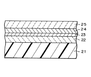
illustrated in Fig. 2, in which reference numeral 21
denotes the polycarbonate substrate, 22 the ZnS
underlying layer, 23 the Sb layer, 24 the InSb layer,
and 25 the UV-cured resin protecting layer. Note the
layers 23 and 24 may be a layer having a single phase,
respectively.
It was confirmed by X-ray diffraction that the
layers 23 and 24 of Sb and InSb were crystalline.
Generally, a layer of an alloy having a uniform chemical
composition is crystallized by heat treatment at about
150C but a laminate of layers of an element or an
intermetallic compound, may be crystallized at a temper-
ature below 100C.
The discs 1, 2, and 3 were rotated at a linear
velocity of 6 m/s, a laser beam having a beam spot
diameter of 1 ~m was used at various powers to record
and read information at 3 MHz with a bit length of 1 ~m,
and a CN ratio (carrier to noise ratio) was determined
in relation to the power of the laser. The results are
shown in Fig. 3. From Fig. 3, it can be seen that the
disc No. 1, which was prepared by evaporation while
heating, has characteristics superior to those of the
disc No. 2, which was prepared by evaporation at room
temperature followed by heat treatment, and disc No. 3
which was prepared by evaporation at room temperature
without a following heat treatment.
Then a laser beam having a beam width of 1 ~m and a
13~48
~eam length of 5 ~m with a power of 10 mW was irradiated
on a recorded track of the discs, and thus the infor-
mation was erased. Then, new information was recorded
on that track and read to give a CN ratio similar to the
first ratio. These recording and erasing operations
were repeated and changes of the CN ratio were checked.
The results are shown in Pig. 4. It is seen from Fig. 4
that the CN ratio of disc No. 3, which was prepared by
evaporation at room temperature without a post heat
treatment, was changed (increased) at the beginning of
the repetition, while those of disc No. 2, which was
prepared by evaporation at room temperature followed by
a post heat treatment, and disc No. 1, which was prepared
by evaporation while heating, were not changed at the
beginning of the repetition. The disc No. 1, which was
prepared by evaporation while heating, has superior CN
ratio in comparison with those of discs Nos. 2 and 3,
which were prepared by evaporation at room temperature.
From the above, it is deemed that heat treatment of
a substrate during evaporation of a recording layer has
advantageous effects on the characteristics of a
recording disc. Further, a time of 1 hour was needed to
prepare disc Nos. 1 and 3, and a time of 3 hours was
needed to prepare the disc No. 2, including the heat
treatment after evaporation. Thus, ~he present invention
has an advantage in that the time for preparation of a
disc is shortened.
Example 2
In the same procedure as in Example 1, a disc
similar to disc No. 1 of Example 1 was prepared except
that evaporation was replaced by sputtering and ion
plating respectively. The resultant discs had a
dependency of the CN ratio on a laser power and a
dependency of the CN ratio on the repeated recording and
erasing similar to those of disc No. 1 of Figs. 3 and 4.
In the sputtering, however, when the deposition
rate was increased to a certain degree, the resultant
1315~8
-- 10 --
InSb layer became amorphous while the Sb layer was still
crystalline. In such a case, a laser beam annealing was
preferably carried out to make the InSb layer crystalline
before an actual operation of the disc. Note, this
laser beam annealing, however, is simpler and shorter in
comparison with a laser beam annealing necessitated
after an alloy of InSb and Sb having a uniform chemical
composition was sputtered at room temperature.
Example 3
In place of the polycarbonate substrate of
Example 1, an epoxv resin substrate, an acrylic resin
substrate, and a glass substrate having a surface
UV-cured resin film, were used to prepare a disc under
the same procedures as in Example 1.
The resultant discs had a dependency of the CN
ratio on a laser power and a dependency of the CN ratio
on repeated recording and erasing similar to those of
the disc No. 1 shown in Figs. 3 and 4.
Example 4
The procedures of preparing the disc No. 1 of the
E~ample 1 were repeated to prepare discs, except that
(1) As and InAs were successively evaporated to form a
recording layer having an average chemical composition
of In3As7 , (2) In and In2B were successively evaporated
to form a recording layer having an average chemical
composition of In7Bi3 , (3) Sb and GaSb were successively
evaporated to form a recording layer having an average
chemical composition of Ga3Sb7 , and (4) Bi and TlBi2
were evaporated to form a recording layer having an
average chemical composition of T125Bi75 , respectively,
instead of Sb and InSb being evaporated to form a
recording layer having an average chemical composition
of In4 6
The resultant disc had a CN ratio of 48 dB at a
linear velocity of the disc of 6 m/s, an recording
signal frequency of 3 MHz, and a laser power of 10 mW,
respectively..
Example 5
The procedures of preparing the disc No. 1 of
Example 1 were repeated, expect that SiO2 , SiO, TiO2 ,
GeO2 , A12O3 , ZnO2 , ZnS, MgF2 ~ CaF2 , Si3N4 ~ AlN and
~N were evaporated to form a protecting layer having a
thickness of 100 nm on the recording layer, in place of
a UV-cured resin protecting layer. The typical CN
ratios of the resultant discs in relation to the laser
power are shown in Fig. 5. The dependencies of the CN
ratio of the discs on repeated recording and erasing
were similar to those of the disc No. 1 in Fig. 4.
Example 6
The procedures of preparing the disc No. 1 of
Example 1 were repeated, except that TiO2 , GeO2 ,
2 ' 2 3 ' Zr2 I MgF2 ~ CaF2 , Si N AlN and
BN were used to form an underlying layer.
The resultant discs had a dependency of the CN
ratio on the laser power and a dependency of the CN
ratio on repeated recording and erasing similar to those
of the disc No. 1 shown in Figs. 3 and 4.
Example 7
The procedures of preparing the disc No. 1 of
Example 1 were repeated, except that Sb and Se were
coevaporated to form an Sb layer containing 5~ by atom
of Se based on the total atoms of In, Sb and Se, in
place of a pure Sb layer, and a disc No. 4 was obtained.
The disc No. 4 had a dependency of the CN ratio on
the laser power and a dependency of the CN ratio on
repeated recording and erasing similar to those of the
disc No. 1 shown in Figs. 3 and 4.
The discs No. 1 and No. 4 were placed in a
thermostat kept at 85C after recording and the change
of the CN ratio of the discs were checked. The results
are shown in Fig. 6. While it is known that addition of
Se into an In4Sb6 recording medium will improve the
lifetime of the storage of information (1987 Spring
Conference of Applied Physics Society, Optical
1 31 5~
Recording, 28a-ZL-l), a similar effect of an addition of
Se in a disc prepared by a process according to the
present invention was confirmed.
Example 8
The procedures of preparing the disc No. 4 of
Example 7 were repeated, except that Se was added to an
InSb layer instead of an Sb layer.
The resultant disc had a dependency of the CN ratio
on the laser power similar to that of the disc No. l
shown in Fig. 3, a dependency of the CN ratio on repeated
recording and erasing similar to that of the disc No. l
shown in Fig. 4, and a change of the CN ratio depending
on the lapsed time similar to that of the disc No. 4
shown in Fig. 6.
Example 9
The procedures of preparing the disc No. 4 of
Example 7 were repeated, except that a 5 nm thick Se
layer was inserted between the InSb layer and the Sb
layer instead of adding Se to the Sb layer.
The resultant, disc had a dependency of the CN ratio
on the laser power similar to that of the disc No. l
shown in Fig. 3, a dependency of the CN ratio on repeated
recording and erasing similar to that of the disc No. l
shown in Fig. 4, and a change of the CN ratio depending
on the lapsed time similar to that of the disc No. 4
shown in Fig. 6.
Example lO
The procedures of preparing the disc No. l in
Example l were repeated, except that the thickness of
the InSb layer was changed to prepare six discs having
various thicknesses of the recording layer. Those
layers have chemical composition of In4Sb6. Then the
reflectivities of the discs were measured. The results
are shown as the line a in Fig. 7.
Discs having various thicknesses of an InSb layer
were prepared in a similar manner to that above, but the
InSb layer 120 to 95 nm) was first evaporated followed
1315S~
by depositing an Sb layer (5 nm) thereon. The measured
reflectivities of the discs are shown as the line b in
Fig. 7.
Discs similar to the above but having a layer with
a uniform chemical composition of In4Sb6 were prepared
with a thickness varying from 20 to 100 nm. The
reflectivities of the discs are shown as the line c in
Fig. 7.
From Fig. 7, it is seen that a disc having layers
of a laminated structure has a wider range of
reflectivity, as shown by the lines a and b, than a disc
having a single layer having a uniform chemical
composition, as shown as the line c, if they have the
same average chemical composition.
As understood from the above description and
examples, according to the present invention, a temper-
ature for crystallizing a recording layer of an alloy
may be lowered so that such a recording layer may be
formed on a plastic substrate susceptible to heat; a
time for preparing a disc may be shortened, since a heat
treatment after deposition of a recording layer is
eliminated; and an excellent crystallized recording
layer of an alloy can be obtained so that the charac-
teristics of the recording medium are improved. Further,
a range of the reflectivity of a recording medium can be
widened in comparison with a disc having a single
recording layer of an alloy having a uniform chemical
composition.