Note: Descriptions are shown in the official language in which they were submitted.
llRC4656
APPAJ~ATIJ3 FOR PROVXDING DIgTANC}3 PROT13CTION
AND I)I8~!ANCB ~BA31J}~EM13Nl!
FOR A ~ H ~O~TAGE TRAN8MI~38:tON I.IN~
BAC~GROIJND OF q~E: INVEN~ION
The present invention relates to protective
systems ~or use in ~C electrical power distribution
systems and more particularly to distance relays for AC
electrical power transmission line protection.
Distance relays are well known in the art of
protective relaying. For example, re~erence may be had
to "The Art and Science of Pxotective Relaying", Mason,
published by John Wiley and Son, Inc. (1956~,
particularly to Chapter 14. Exemplary types of
distance relays are disclosed in U.S. Patent No.
4,034,269, issued to S~ B. Wilkinson, on July 5, 1977;
U.S. Patent No. 4,420,788, issued to S. B. Wilkinson
and G. E. Alexander on December 13, 1983; and U.S.
Patent No~ 4,405,966, issued to Leonardo Cavero, the
inventor of the present invention, on September 20,
1983. All these patents are assigned to the assignee
of the present invention.
Distance relays are utilized in
protective systems or AC power transmission
lines to detect faults within protected
zones or portions of the transmission lines. If
--1--
:~ 3 ~
llRC4656
such a ~ault i3 detec~Qd wi~hin ~hQ relay~s æon~ ar reach,
~he distance relay ~i~l enable op~ration o~ a circuit
breaker in order to trip the faulted phase or phases.
Phas~ distance relay~ are u~ z~d to de~ec~ phase
to phas~ faults wi~hin a protec~ed zone or portion of a
~rans~ission llne. I~ such a ~ault is detec~ed wi~hin the
zone or reach o~ this type of distance relay, ~he phase
d~stanca relay will initiate a ~ignal which will be used to
cause the operation of a three pole circui~ ~reaker to trip
all three phase~ of the transmission line. This is to ~e
contrasted with a ground distance relay which detects
faults be~ween a phase and ground,~ again within a
designated zone or reach; and, upon detection o~ such a
fault, g~nerates a signal which enables the operation o~ a
circuit breaker to trip the faulted phase only.
As indicated above, each particular distance relay
should only detect faulks wi~hin its protected zone or
reach. The parameters of a distance relay are commonly
selected to correspond to ~he parameters of the
transmis~ion line. For example, the parameters are
selected to provide a forward reach tha~ may correspond to
the ~orward distance o~ the proteGted zone o~ a
transmission line under protection of the particular
relay. It is desired that the distance relay operate
5 within its selected ~orward reach thereby confining the
-2-
ll~C4 656protectiorl o~ a part~ ular di!3~ance relay ~o ~he select~d
zone within a protected sy~
The desired operation o~ the ~i~;tanc~ relay may be
hindered by the inability to di~3tirlguish between internal
5 and e~ernal îault~ nterllal ~aul~s are 1:ho~e which oc~r
within the protected zone or rQach o~ the relay, whereas
external faults are th08a which occur ou~:1 de the zone or
relay r~ach. For exaDIple, errors in measuring fault
re~istarlce can cau~Q th~a ~ault to appea:r ~ur~her away from
10 or closer to the distance relay location than it actually
is: situation3 whlch, in the worse case, collld preYent the
operation of the distance relay on ~ fault occurring within
its zone or reach, or could cause the relay to misoperate
for a fault external to the protected zone or reachO
Although distance relays haYe, in the past, been
used to dete~t faults within a predetermined protec:ted zone
or reach o~ the relay, such relay.~ have not ~een able to
provide a determination of the actual location of the
fault: that is, the distance from the relay at which the
20 fault occurred. ~he ability to determine th~ location of
the fault in terms o~ distance from the relay enhanc~s the
utility of a distance relay.
--3--
~ 3 ~
llRC4656
Accordingly, it læ an o~ect of th~ pre~ent
invention to provida a ~is~ance relay wit~ improved
discrimination between in~e~nal and external faults thareby
increasing thQ reliability o~ ~he relay opera~ion and the
security of th~ protect~on 5y5tem.
It is another ob~e~t of ~he present invention to
provide a dlstanc~ xelay for detecting faults in a
protected zone of an AC electrical power ~ransmission line,
which relay determlne.~ the dis~ance to the fault.
It is yet another object of the present invention
to provide a distance relay with a capability for i~proved
fault resistance determination~ ~
It is a ~urther object of the present in~ention to
provide a distance relay which substantially eliminates the
adverse effects on fault d~stance determination due to
fault current co~ponents from multipl~ sources connected to
the AC power trans~ission line.
It is still another o~ject o~ the present
invention to provide a distance r~lay which eliminates
adverse effects of prefault load current on fault distance
determination.
These and other abjects of the present invention
-~ill become apparent to those skilled in the art upon
consideration of the following description of the
invention.
-4-
~ 3 ~
llRC4656
The present i~ven~ion compriseg a distance relay
for detec~ing ~aults within a predetermined protected zone
o~ an ~c electrical power ~rans~i~ion line and for
~easuring the distance to detecte~ ~aults. The distance
relay includes mean~ for detecting a ~ault current and
subtracting pre~ault current there~rom.
Th~ eature~ o~ the invention belie~ed to be
n~vel, are sQt ~orth particularly in the appended claimsO
The invention itself, however, bo~h as to its oryaniæation
and operation, together with further objects and advantage~
~hereo~, may best be understood by~reference to the
following description in conjunction with the accompanying
dra~ing figuresO
. }3aIEF_DE8CR~l?T:~O~ OF ~IE DRAW~:NGi%
Figure 1 is a one line, ~lock diagram o~ a current
and voltage pracassing portion of a preferred embodiment of
the present invention.
Figure 2 is a bloc~ diagram of a first operate
signal genexation portion of the preferred embodiment of
the present invention, utilizing voltage and current
signals generated by that portion depicted in Figure 1.
llRc46s6
Fiyur~ 3 i~ a block dlagra~ of a distance
measurement portion o~ ~he preferred embodimen~ o~ the
pres@nt invention, utilizin~ vol~age and current signals
generated by the portion depicted in Figure 1.
Figure 4 is a block diagram o~ a second op~rate
signal gen~ration portlon o~ the pre~erred embodiment of
the present inventlon, utilizing voltage and current
~ignals generated by that portion depicted in Figuxe 1.
Figure 5 is a bloc~ diagram of a ~rip signal
generation portion oP the preferred embodiment o~ the
present invention, ut~lizing th~ firs~ and second operate
signals generated by that port~on *epicted in Figures 2 and
4 respectively.
Figure 6 depicts the characteristic of the
preferred embodi~ent of the relay of the present invention
plotted on an L-R diagram.
Figure 7 is a block diagram of a third operate
signal generation portion of the pre~erred em~odiment of
the present invention, utilizing a delta current signal
generated by that portion depicted in Figure 1 and signals
generated by the second operate signal genera~ion portion
depicted in Figure 4.
Figure 8 is a one lin~, block diagram of an
current and voltage processing portion of an alternate5 preferr~d ~mbodiment of the present invention.
-6-
llRC4656
Figure 9 i a block diagra~ o~ a dls~ance
~impedance measurement portion o~ the alternate pre~erredembodiment o~ the pre~ent invention9 utilizing voltagQ and
curren~ signals generated by that portion depicted in
Figure 8.
Figure 10 is a block diagram o~ a di~tance
protectio~ portion oS the alternate pre~erred embodiment of
the pres~nt inve~tion, utilizing voltagQ and current
signals generated by ~hat portion depicted in Flgure 8.
Figure 11 i5 a block diagram of a distance
protection, re istance reach and mea~urement portion of the
alternate preferred e~bodiment of ~he present invention,
utilizing voltage and current signals generated by that
portion depicted in Figure 8.
Figure 12 is a block diagram of a trip signal
generation portion of the altexnate pre~erred embodiment of
the present invention, utilizing the operate signals
gen~rated by that portion depicted in Figures 10 and 11.
Figure 13 depicts the characteris~ic of the
20 alternate preferr~d embo~i~ent of the relay of the present
invention plott~d on an L-R diagram.
Figure 14 is a block diagram of a preferred
e~bodiment o~ a fault resistance measurement portion of the
present invention.
~3 ~ ~ar~
llRC4656
Figura 15 i a bloc~ diayram of an alternate
pæeferrsd embodi~ent o~ a re~is~ance measurement porkion of
~he present in~ent~onO
D~ D l~ :L~ P~FB~RBD E~pD~B~
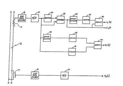
Referring to Figure 1, there is shown an
alternating current ~lectric power transmission line,
generally designa~efl 10~ Although such alterna~ing ourrent
ele~trical power ~ransm~ssion lines nor~ally co~prise three
phases and ground, for purpose o~ simplicity and clarity,
th~ following d~ailed description will ~e described with
respect to the A phase (A) and ground (G). It should be
understood that ~he following description also applies wi~h
respect to th~ B and the C phase, as well a~ relays
ccnnected between phase~
Associated with A phase is means lZ for sensing
current in that phase as well as means 14 for sensing
voltage on t~ak phase. As is well known to those skilled
in the protectiYe relaying an~ power transmission art,
current sen~ing mean~ 12 may be a current transformer and
~o voltage sensing means 14 may be a step down potential
transformer. Also, a curr~nt sensing means may be
associated with each phase as well as a separate
~ 3 ~
llRC4~56
voltage sensing means associated with each phase. However,
it is to be understood that although a speci~ic type o~
current and voltag2 sen~ing scheme is depicted in Figure 1,
o~her s~hem~ known in the ar~ may bs substituted for that
depicted; th~ purpoæe being to obtain signals which are
relat~d to each phase voltage and each phase current,
The output from the current sensing means 12,
which is a signal iA(t1 proportional to the currenk
~lowing in tha A phase, is coupled to the input o~ a first
low pass ~ilter 16. The output of the voltage sensing
mea~s 14, whic~ is ~ signal ~(t) proportional to the
phase A to ground voltage, is coupIed to the input of a
second low pass filter 18. In the preferred embodiment,
the first 16 and second 18 low pass filters each preferably
have a frequency cut off of approximately 500Hz in order to
filter out transients and other spurious signals having
~requencies which exc~ed lKXz, while passing, substantially
unchanged, signals at the system frequency which is
typically 50Hz or 60Hz. Consequently, the output signal
iA(t) from the first filter 16 is the filtered input
signal iA(t), and the output signal vA(t~ fro~ the
second filter 18 is the filtered input signal v~(t).
The output vA(t) o~ the second low pass ~ilter
18 îs coupled to the input of a ~irst analog to digital
(A/D) converter 20. In the preferred embodiment, the first
_g_
~ 3 ~
llRC4656
A/D converter 20 sample~ tha magni~ude o~ the input signal
at a predetermined ra~e which in ~he preferred embodiment,
is twenty samples per cycle in 50Hz systems and six~een
samples per cycle in 60 ~z sy5~ems. The magnitude o~ each
sample is converted in~o a digital signal having a value
corresponding to such magnitude. consequen~ly, the output
vA(t) o~ the first A/D conver~er 20 i5 a digitized
version o~ the analog input signal.
The output of th~ *irst low pass filter 16 is
coupembodiment, the second A/D converter 22 i5 of the same
type and performs th~ sa~e function a~ that previously
described with respect to the first A~D ConYerter 20. The
output i~(t1 of the second A/D conver~er 22, which is a
digitized version o~ the input ~ignal, is coupled to the
input of a buffer 24, a positive input of a first digital
subtraction circui~ 26, the input of a first differentiator
28, and the input of a firs~ scaler 30. In the preferred
embodiment, the buffer 24 comprises a memory for storing
the digitized input signal iA(t) for a time kt~ wh~re k
is a predetermined constant and f is the system freguency,
typically 50 Hz or 60 Hz. Ac~ordingly, the outpu~ of the
buffer 24 is the signal iA(t-k/~). When k=l, the output
of the buffer 24 is equal to the magnitude of iA at a
point one cycle prior to the input iA(t). In the
preferred embodiment, the output iA(t-k/f) of buffer 24
is the input signal iA(t) which has been delayed five
--10--
~ lr~8/~
llRC4656
cycles at the funda~ental syste~ ~requency; thak is, 100
milliseconds in a 50Hz system and ~3.333 mllliseconds in a
60Hz system.
The output i~(t-k/r) o~ ~he buffer 24 is coupled
to a negative input of the ~irst digital su fflraction
circuit 26. In the pr~erre~ embodimen~, the ~ir~t digital
subtraction circuit 26 i~ a circuit whose output i5 a
digital signal a iA(t) ha~ing a digital value equal to
the ma~nitude o~ the digital value o~ the input signal
applied to the positive input minu the value of the signal
applied to the negative input. Sinc~ the signal i~(t) is
applied to the positive input and the signal iA(t-k/f) is
applied to the negative input, the output signal,
~iA(t) is egual to iA(t)-i~(t-k/~. ThP output
15 ~iA(t) of the digital subtraction circuit 26 is ~oupled to
~he input of a second dif~erentiator 32 and one input of a
first two-input adder 34. In the preferred embodiment, the
first 28 and second 32 differentiators each measures and
stores the ma~nituda of the input signal at a first time
tl and again at a second time t3, then subtracts the
magnitude measured at t~ from the magnitude measured at
t3 and di~ides the result by the magnitude of time t3
minus time tl. Consequently, the output of the second
digital differentiator 3Z is a signal
d ~ A(t) at a time t2, having a value su~stantially equal
llRC4656
to the di~ferentlal, with respect ~o ~ime 7 0~ the input
signal ~ iA(t).
The output o~ the second digital dirferentiator 32 i5
coupled to the input o~ a seco~d s~aler 36. Th2 second scaler
36 is a circuit whose output i8 ~ digi~al signal having a
magnitud~ equal to ~h~ lnput signal
d a iA(t, ~ltiplied by a predete~mined scaler function
.
dt
which, in the pre~erred embodiment is ~ , where f is the
2 4~ f
fundamental syste~ frequency, typically 50~z or 60Hz, and
tan O~ is a quantity which is a fu~ction of ~he particular
power system in which the distance r~lay o~ the pre~ent
invention is used. Consequently the output
of the second scal~r 36 is d ~ iA(t3. tan~ .
.
dt 2~f
The output of the second scaler 36 is coupled to
the second input of the first two-input adder 34. The
first two-input adder 34 is a circuit whose output is a
digital signal i~(t1 having a magnitude which is e~ual to
the digital sum of the input signals which are
iA(t) and d iA(t? ~an ~.
dt 2 ~ f
Consequently, the output if(f) of the first two-input adder 34
is e~ual to ~ iA(t)+d ~ iAtt) tanc~.
_ _ . _ . ......
dt 2
-12-
~ 3~.~8~
llRC4656
The output o~ the f irst di~erentiats: r 2~ i~ a
digitzll signal d~t~ whose magni~de is tA~ di~rerl~ial
_.
dt
respect to time o~ the ~nput signal i~(t). The output
diA~t)
dt
of ~hQ first di~ferentiator 28 is coupled to the input o~ a
third scal~r 38. The ~hird scaler 38 is o~ the same type
as that previously de$crihed with respect to the first 30
10 and sec:ond 3 6 scalers, having a digital ou~put signal
whose magnitude is equal to the input
diA(t) multiplied by a prede~e~mined æcaling function which,
dt
in the preferred embodiment, is Lo Consequently, the5 output o~ the third -~caler 38 is LdiA(t)~
dt
The magnitude o~ L is selecte~ to be substantially equal to
the line inductance per mile o~ the particular power system
in which the relay o~ the present invention is used.
0 The output LdiA(t~ o~ the third scaler 38 is coupled
dt
to one input of a second ~wo input adder 40.
-13-
~3~5~
llRC4656
The output o~ the fir ~ scaler 30 is a digital
signal whosQ ma~nitude is equal to the input signal i~t)
mu?.tiplied by a predeter~ined scaling Punction which, in
th~ pre~erred e~bodiment, i~ ~. Conseguently, the output
of the ~irst scaler 30 is R~ ) . The mat~nitude o~ R is
selecked to be sub tan~ially equal to ~he line resistance
per mile of th~ part~cular power system in which the relay
of the present invention is used. ~he output Ri~(t) of
the first scaler 30 is coupled to the second input of the
second two input adder 40. The second ~wo input adder 40
is the same type as that previously described with respect
to tha first two input adder 34, havin~ a~ output signal
whose magnitude is egual to the sum
of the inputs RiA(t) and LdiA(t). ~ccordingly, vr(t)
dt
is equal to RiA(t~LdiA(t).
dt
Referring now to Fig. 2, the output signal if(t)
from the first two-input adder 34 (see Fig. 1) is coupled
to the input o~ the ~ir.st sampler/buf~er circuit 42. The
output vr(t) from the second two-input adder 40 (see Fig.
1) is coupled to the input of a second sampler/buf~er
circui~ 44. The output vA~t) of the first A/D con~erter
20 (see Fig. 1~ is coupled to the input of a third
sampler/bu~fer circuit 46~ In the preferred embodiment,
the first 4Z, second 44 and third 46 sampler/buffer
-14
~ 3 ~
llRC4656
circ~aits each ha~ 3 two outputs, the ~irst of whis:h is equal
to the magnitudE~ o~ the inpu~ signal sampled at a f ~ rst
time t1~ and the se~ond of which i8 eyual ~o the
magnitude of the input signal sampled at a second tlme
t2. Consequently, ~he outputs o~ the firsk
sampler/buffer circuit 42 is a firs~ signal i~(tl~
which is the i~put signal i~(t3 sampled at time t1; and
the sacond output is a signal if(t2) which is equal to
the input signal i~t~ sampled at time t2o
Similarly, the outputs of th~ second
samplerJbuf~er circuit 44 co~prise a first sig~al
vr(tl) which is equal to the input signal vr(t)
sampled at the first ti~e tl; and a second signal
vr(t2) which is equal to ~he input signal vr(~)
15 sampled at the second time t2. The outputs of the third
sampler/~uffer circuit 46 comprise a first signal
vA(tl) which is equal to the input signal vA(t)
sampled at the first time tl; and a second signal
vA(t2) which is equal to the input signal vA(t)
20 sampled at the second time t2.
The output signal if(tl) from the first
samplerJbuffer circuit 42 is coupled to one input of a
~irst two-input ~ultiplier 48 and one input of a second
two-input multiplier 50. The output signal if(t2) from
25 the first samplerJbuffer circuit 42 is coupled to one input
-15-
o 4 b~
llRC4656
of a thixd two-input multiplier 52 and one input of a
four~h two-input multipli~r 54. The ou~pu~ signal
vr(tl~ from ~he s~cond sampler~buf~er circui~ 44 is
coupled to ~he second inpu~ o~ the third two~input
multiplier 52. Th~ output signal vr~t2) from the
seeond sampler/bu~er circuit 44 is couple~ to the second
inpu~ of the first two-input ~ultiplier ~ he output
signal v~(tl~ from the third sampler/buf~er circuit ~6
is coupled to the second input of the fourth two-input
10 multiplier 54. The output signal ~A(t2) ~rom the thlrd
sampler/bu~fer circuit 46 is coupled to the second input of
the second two-input multlplier SO.r
In tha preferred e~bodi~ent, the first 48, second
50, third 52 and ~ourth 54 two-input multipliers are each
15 digital multipliers producing a digital output signal
having a magnitude which is equal to the magnitude of the
first.input si~nal multiplied by the magnitude of the
second input signal. Consequen~ly, the output of the first
multiplier 48 is the signal vr(t~ (tl); the
20 output of the second multiplier circuit 50 is the signal
VA(t2)if(tl); the output of the third multipliex 52
is the signal vr(tl)if(t2); and the output of the
Pourth mulkiplier 54 is the signal v~(tl) if ~t2) .
-16-
llRC4656
The output of the firs~ mul~iplier circuit 48 is
coupl~d to a negative input of a second digi~al sub~raction
circuit 60. The output of the second multiplier circuit 50
is coupled to a negative input of a third digital
subtrac~lon circuit 62. The su~pu~ of the third multiplier
circuit 52 is coupled to a positiYe input of the second
digital subtraction circuit 600 ~he output of the ~ourth
multiplier circuit 54 is coupled to a positive input of the
third digital subtra~tion circuit 62. In the preferr~d
em~odiment the s~cond 60 and third 62 digital subtraction
circuits are of the same type as the previously described
~irst digital subtraction circuit ~6, each producing a
digital output siynal whos~ magnitude is equal to the
magnitude of the signal applied to the positive input
minus the magnitude of the signal applied to the negative
input. Consequently, the output of the second digital
subtraction circuit 60 is the signal Sl which is
i5 egual to vr(tl)if(t2)~Vr(t2~if(tl); and
the output of the third digital subtraction circuit 62 is
the signal S2 which is equal to
VA(tl) if (t2) -VA(t2) if ~tl~ -
--17--
~ 3~
llRC4656
The output signal Sl ~rom the ~cond digitalssbtraction circuit 60 1~ coupled to the input of a four~h
scaler ~ircuit 64. The ~ourth scal~r cir~ui~ 64 is
preferably o~ the sa~e trpe as that previou-~ly described
with respect to the first 30, second 36 and third 38 scaler
circu~ts, having an output which is equa~ ~o the input
multiplied by a predeter~ined scaling function. In the
pr~ferred e~bodi~entt the scaling ~unction o~ the fourth
3caler circuit 64 is the quantity nSe~ which i~ a
constant determined by ~he desired r~lay reach.
Consequently, ~he output Q~ the Pourth scaler circuit 64 is
the signal
nset(Vr(tl)if(t2)-vr(t2)i~(tl))
or ~5etsl .
- The output of ~he fourth scaler circuit 64 is
coupled to a first input of a ~irst two-input comparator
circuit 66. The output of the third digital ~ubtraction
circuit 62 is coupled to a second input of the ~irst
two-input comparator circuit 66. The first two-input
comparator circuit 66 is a digital comparator which
generates an output signal when the magnitude of the signal
applied to the first input exceeds the magnitude of the
~ignal applied to the second input. Consequenkly, the
first two-input comparator circuit 66 generates an output5 signal when the ~aynitude of the signal
-18-
llRC4656
ns~t{Vr(tl~ 2)~Vr(lt2)i~(tl)) exceeds
~he magnitude o~ ~he signal
~A(t~ (t2)~V~(~2)if(t1~} or
nse~Sl>S2 -
The output o~ the f ~ rst two-input co~parator
aircuit 66 is coupled to thQ input of a irst counter 68.
In the preferred embodi~ent, the first coun~er 68 provides
a count signal upon receipt of a signal fro~ tha ~irst
two-inpu~ comparator circuit 66. The count signal is
incremented by one count i~ the signal ~rom the cixcuit 66
is prssent during the ne~t succeeding sa~pling interval;
otherwis~, the count signal is re~et to zero. The count
signal is incremented by one count upon receipt o~ a signal
from circuit 66 during each succeeding sampling interval~
The count signal is reset to zero follow~ng any sampliAg
interval durin~ which a signal i~ not receiYed ~rom circuit
~6.
The count signal from the first counter 68 is
coupled to the input of a first comparator circuit 70. The
first comparator circuit 70 generates an output signal
1~ which is a first operate signal in the preferred
embodiment described herein, when the Magnitude oP the
input signal exceeds a predetermined value. Consequently,
the first comparator circuit 73 will generata the first
~perate signal l when th2 magnitude of ~he coun~ signal
19--
..
t~l~)t~
llRC4656
from th~ counter 68 exceeds a predQ~e~min~d value, ~or
exa~pl~ ~hree in ~hQ pre~erred embo~imen~. Thi~ means that
in th~ pre~rred em~odimen~, the firs~ opera~e sig~l l
will be generated upon detec~ion nf a sig~al ~rom the first
two-input co~para~or circuit 6~ during at leas~ three
consecutiv~ s~mpling interv~ls.
Referring now to Figure 3, th~ output signal
~iA(t) ~rom the first diyital subtraction cir~uit 2fi (see
Figure 1) i8 coupled to the input of a ~ourth
sampler/bu~er c~rcuit 202. The ou~pu~ Vr(~) ~rom the
s~cond ~uo input adder 40 (see Figure 1) i~ coupled to th~
input of à fi~th sampler/buffer circuit 204. The ou~put
v~(t) of th~ first A/D converter 20 (see Figure 1) is
coupled to the input of a sixth sampler/buf~er circuit
206. In the preferred em~odlment, the fourth 202, fifth
204 and sixth 206 sampler/buf~er circuits are o~ the same
~ype as ~he firs~ 42, second 44 and third 46 sampler/buf~er
circuits previously described. Each has two outputs, the
first of which is equal to the magnitud~ o~ the input
signal sampled at the first time tl, and the second o~
which is equal to the magnitud~ of the input signal sampled
at thQ second ti~e t2. Consequently, the outputs of the
fourth sampler/buff~r circuit 20~ is a first signal
~iA(tl) which is the input signal
-20-
llRC4656
~ iA(t) sampled at thQ ~irst ~ime ~1 and ~he second
output is a signal ~ (t2) which i~ equal to the input
signal a i~(t) sampled at the ~eco~d time t2.
~imilarly~ tha ou~put~ of th~ f$~h sampler/bu~er
c~rcuit 204 co~pri~Q a ~irs~ signal Vr(t1~ which is
equal to th~ input signal Vr(tj sa~pled at ~he firs~ time
tl; and a second signal Vr(t2) which is equal to the
input signal Vr(t) s~mpled at the second tim~ t2 ~he
outputs of the six~h sampler/buffer circuit 206 comprise a
first signal v~(tl) which i5 equal to the input signal
vA(t) sampled at ~he first time t1; and a second signal
vA(t2) which is equal to the input signal vA(t)
sampled at th~ second time t2.
The signal ~iA(t1) output from the fourth
sampler/buffer circuit 202 is coupled to one input of a
fifth two-input multiplier 208 and one input o~ a sixth
two-input multiplier 210. The signal ~ iA(t2) output
from the fourth sampl~r/buffer circuit 20Z is coupled to
one input of a seventh two-input multiplier 212 and one
input of an eighth two-input multiplier 214. The
Vr(t1) signal output from the fifth sampler/buffer
circuit 204 is coupled to the second input o~ the seventh
two-input multiplier 212. The signal Vr(t2) output
from the fifth sampler/bu~fer cir~uit 204 is coupled to ~he
second input o~ the fifth two-input multiplier 208. The
-21-
1 3 ~
c46s6
signal v~(tl3 output fro~ the ~ix*h sampler/bu~X~er
circuit 206 i~ coupled to thR second input o th~ eigh~h
t~o-input ~ultipl~er 214. ~h~ signal vA(t2) output
fro~ the sixth sa~pler/bu~er circuit ~06 is coupled to the
second input of the sixth two input multiplier 2100
In the pre~erred e~bodim~n~, the ~if~h 20~, six~h
210, seventh 212 and eighth 214 two-input multipliers are
the sa~s type a~ the ~irst 48, sa~ond 50, third 52 and
fourth 54 two-input Dlultipliers previously descri~ed. Each
10 two-input multiplier produce~; a digital output signal
having a magnitude which is equal ~o the magni~ude of the
first input signal multiplied by the ~agni~ude o~ the
second input signal. Consequently, ~he output o~ the fifth
multiplier ~08 i~ the signal Vr(t2)~ iA~tl); the
output of the sixth ~ultiplier circuit 21D is the signal
vA(t2)~iA(tl): the output of the s~venth
multiplier 212 is the signal Vr(t~ iA(t2); and
the output of the eig~th multiplier 214 is the signal
VA ( t~ A ( t2 ) -
The output of the fifth multiplier circuit 208 is
connected to a negative input of a fourth digital
subtraction circuit 21~. The output of th~ sixth
multiplier circuit 210 is coupled to a negative input of a
fifth digital subtraction circui~ 218. The output of the5 seventh multiplier circuit 212 is coupled to a poæitive
-22-
~ 3 ~
llRC4656
input o~ tha ~ourth digital sub~raction circuit 216. Theoutput of ~he eighth multiplier circuit 214 is coupled to a
positive input o~ the ~i~th digi~al subtrac~lon circuit
218. In thQ prefexred e~bodimenk, the fourth 2~6 and ~ifth
218 digital subtraction circuits are of the same ~ype as
the pr~iously da~cribed ~irst 26, second 60 and ~hixd 62
digital subtractlon circuit~, with each producing a digital
output signal whosQ magnitude i5 equal to the magnitude o~
the signal applied to the positive input minus the
magnitude of the sig~al applied to th~ negative input.
Conseguently, the output signal S3 o~ the fourth digital
subtraction circuit 216 is e~ual to
Vr(tl)~iA(~2)~Vrtt2)~iA(tl); and the output
signal S4 og the fifth di~ital subtraction circuit 2~8 is
equal to VA(tl) a iA(t2) -V~(t2) ~ A(tl) .
The output signal S3 o~ th~ fourth digital
subtraction circuit 216 is coupled to the divisor input of
a digital divider circuit 220. The output signal S4 of
the ~ifth digital subtraction circuit 218 is coupled to a
dividend input of the digital divider 220. The output n
from the divider circuit 220 is a digital signal whose
magnitude is equal to the quotion of the digi~al signal
S4 applied to the dividend input divided by the digital
signal S3 applied to the divisor input~ The magnitude of
the signal n is a function of the distance ~rom the relay
to the fault and is equal to
-23-
~ 3 ~
llRC4656
Va(t~ t2)-VA(t2)~iA(tl) S4
Vr~t~ A(~2)~Vr(t2j~ iA~tl) S3
Re~erring now to Figure 4; ~he ou~put signal
iA(t) ~ro~ the ~irst digital s~tract~on circuit 26 (see
Figure 1) i~ coupled to th~ input o~ a seven~h
sampler/bu~fer circuit ~02. T~e output Vr~t) from ~he
sacond two-input adder 40 (see Figur~ coupled to thQ
input o~ an eighth sampler/buffer circuit 404. The output
vA(t) of the first A/D converter 20 (see Figure 1) is
coupled to the input o~ a ninth sampl~r~buffer circuit
406. In the preferred ~mbodiment, the seventh 402, eighth
404 and ninth 406 sa~pler~buffer circuits are of th~ same
type as the first 42, s~cond 44, third 46, ~ourth 2C2,
~ifth 204 and sixth 206 sampler/bu~er circuits previously
described. Each has two outputs, ~he fixst of which is
equal to the magnitude oP the input signal sa~pled a~ the
first time tl, and the second o~ which is equal to ~he
magnitude of the input signal sampled at the second time
t2. Consequently, the outputs of the seventh
sampler/buffer circuit 402 is a first signal ~iA(t1)
which is t~e input signal ~ iA(t) sampled at the first
time tl; and the second output i a signal A iA(t2)
which i~ equal to the input signal A iA(t) sampled at the
second time t2.
~ .
-24-
$~
llRC4656
Similarly, th~ output8 0~ the eighth
samplerjbuffer circuit 404 co~prises a ~irst signal
Vr(tl) which i~ equal to the input signal Vr(t~
sampled at the ~irst time t~; and a second signal
Vr(t~) which is equal to the input signal Vr(t~
sa~pled at th~ second ti~e t2. The output~ of ~he ninth
sampler/buffer cix~uit 406 compris~s a Pirst signal
vA(tl) which is equal to the input siynal vA~t)
sampled at the ~lrst time tl; and a seco~d sig~al
vA~t2) which is e~ual to the input signal vA(t)
sampled at the second time t2.
The signal a iA(tl) output fro~ the seventh
sa~pler/bu~er circuit 402 is coupled to one input of a
two-input ~ultipl~r 408. The signal ~iA~t2~ output
fro~ the seventh sampler/bu~fer circuit 40~ is coupled to
one input of a tenth two-input multiplier 410. The
Vr(tl) signal output from the eighth sampler/~uffer
circuit 404 is ooupled to the second input of the tenth
two-input multiplier 410 and to one input of an eleventh
two-input multiplier 412. The Vr(t2) signal output
from the eighth sampler~bu~fer circui~ 40~ is coupled to a
second input of the ninth two-input multiplier 408 and one
input of ~ twelfth two-input multiplier 414. The
vA~tl) signal output from the ninth sampler/buffer
5 circuit 406 is coupled to a second input o~ the twelfth
-25-
13~s8~
llRC4 656
two-input multiplier 414- The va,tt2~ sigrlal output
fr~s~ the n nth sampl~r~bufrer circuait 406 i~ coupled to a
s~cond input of thQ ~l~venth kwo input mul~ipli2r 412.
pref~rred a~bodiment, th~ ninth 408, tenth
410, ele~enth 412 and tw~ 41~ t~o~ puk ~ulti.pliers are
the same type as ~he ~lrgt 48 through eigh~h 214 ~uo-input
multiplier~ previously de3cri~ed. ~:ach ~wo-input
mul~iplier produce~ a digi~al output signal haYing a
magnitud~ ~hich i~ equal to the magnitudQ of the ~irst
input signal mult$pl ~ ad by ~:he Dlagni~ude Or the second
input signal. Consequently, the output of the ninth
n.ultiplier 408 is thQ signal vr(t2) ~ iA(tl); the
output of t:he tenth multiplier ~10 is ~he signal
vr~tl) ~iA(t2); the output of the aleventh
~ultiplier 412 is th~ signal v~(t2 jvr(tl); and the
output of th~ twelfth ~nultipl~ er 414 is the sigrlal
vA(tl)~rr~t2)-
The output of the ninth multiplier circuit 408 is
connected to a po~itive input of a ~ixth digital
subtraction circuit ~16. The output of the ~enth
multiplier circuit 410 is coupled to a negative input of
~he sixth digital subtrac~ion circuit 416. The outpu~ of
the eleventh multiplier circuit 412 i8 coupled to a
n~gative input of a seventh digital subtraction circuit
25 418. TAe output of tAe twel~th multiplier circuit 414 is
-2~-
llRc4656 ~3
coupled to the positlvQ input thla sQventh digital
su~tractioll circuit 418. In the preferred embodiment, the
sixt~ 416 and sevelath 418 digital subtxae~ion cixclaits are
of the sa~n~ type a~ the previou~ly d~3cribed ~ixst 26,
se~ond 60, third 62, ~our~ 216 and fi~th 218 digital
su~traction cir~itsj wi~h each pro~iding a ~igital ou~put
signal whos~ magnitudQ is equal to th~ ~agnitude of the
signal applied to th~ po.itivQ input Dllinus ~he loagnitude of
thc signal applied to thQ negative input. Consequently,
the output si~nal 55 of the sixth diqital slabtraction
circuit 416 i~ equal to vr(~2)AiA(tl)-
vr(t1) ~ ~(t2); and the output signal S6 ~ the
seventh digital subtraction circ:uit 41~ is equal to
~rA ttl) Vr (t2 ) -VA (t2 ) Vr (tl ) -
Tha output signal S5 o~ th~ sixth digital
subtraction circuit 416 i~ coupled to the divisor input o~
a second digital divider circuit 420. ~he output signal
S~ of the seventh digital subtraction circuit 418 is
coupled to a dividend input o~ the second digital divider
420. In the preferred embodim~nt, the s~cond digital
divider 420 is the same type as the previously descri~ed
first digital divider circuit 220; having an output signal
which is a digital signal whose magnitude is equal to the
quotion o~ the digital signal S6 applied to the dividend5 input divided by the digital signal SS applied to the
-27-
llRC4656 3~S~
divisor inputO Con~equ~ntly~ the outpuk R~a from thssecond di~ider circuit 420 i~ equal ~o
~ l)Vr(~2~ (t2)~rttl) S5
v ~ 56
The signal R~ i a fun~t~on o~ the fault r~istance;
that i~, th~ ~a~nitude of ~A i~ proportional to the
~agnitude oP the ~ault re~i~tana~ ~easured at thQ relay
location and the angle o~ tha signal R~A ls substantially
equal to the fault re~istance angle.
The output sign~l S5 o~ the sixth digital
subtxact$on circuit 416 i~ also coupled to the input of a
~ifth scaler circuit 422. The ~i~th scaler circuit 422 is
preferably o~ ~he same type as that previou~ly descri~ed
wi~h respect to the ~irst 30, s~cond 36~ third 38 and
fourth 64 scaler circuits, having an output which is equal
- to the input multiplied by a predetermined scaling
function. In the preferred e~bodiment, the scaling
function o~ the fifth scaler circuit 422 is the quantity
RS~T which is a constant determined by the desired relay
reach. Conse~u~ntly, the output of the fifth scaler
circuit 222 is the signal
RSET~ a iA(tl)Vr(t2)- ~iA(t2)Vr(~l)]
or RSETS5-
-28-
- 1 lRC4 65 6
The output of the fi~h ~caler circui~ ~22 is
couplad to a first input o~ a ~econd two-input cnmparator
circuit 424. T~e outpu~ signal S~ of the seYenth digital
subtraction circuit 41~ i~ coupled to a second input of ~he
second two-input compara~or clrcuit 424. ~he second
~o-input co~parator circuit 42~ i~ pre~erably of ~he same
type as that previously d~cri~ed wit~ re~pect to the first
two-input comparator circuit 66 which generate~ an output
signal when ~he magnitu~e of ~he signal applied to the
~irst input exceeds the magnitude o~ ~he signal applied to
the second input. Consaquently, the second two-input
comparator circuit ~24 genera~es an outpu~ signal when the
~agnitude of the signal
RSETL ~ iA(tl)Vr(t2)- ~iA(t2)Vrttl) ]
excee~s the magnitude o~ the signal
~VA(tl)Vr(t2)-vA~t2)v~(tl) J
or RsETss~s6-
The output o~ the second two inpu~ comparator
circuit 424 is coupled to the input of a second counter
426. In the preferred em~odiment, the second counter 426
is of the same type as that previously described with
- respect to th~ first counter 68 which provides a count
signal upon receipt of a signal ~ro~ the second two-input
coMparator circuit 424. The count signal is incremented by
-29-
- 11RC4656
one count iS th~ signal ~rom th~ second two-input
comparatox circui~ ~2~ 15 prQ~ent durlng ~h~ nex~
succeeding ~ampling interval; otherwise, th~ coun~ signal
is reset to zero. The count si~nal is incremented by one
count upon receipt o~ a signal from the se¢ond tws-input
comparator circuit 424 during each succPeding sa~pling
interval. ~ha count signal is resat to zero following any
sampling interYal during which a signal i5 not received
from tha circuit 424.
Th~ count signal from t~e second counter 426 is
coupled to ~he input o~ a second comparator circuit 428.
The second comparator circuit 428 is preferably of the same
type as that previously described with re pect to khe ~irst
comparator circuit 70 which generates an output signal
15 2 ~ which i~ a second operate signal in the preferred
embodiment, wh~n the magnitude of the input signal exceeds
a predetermined value. Consequently, the second comparator
circuit 428 will generate the second operate signal 2
when t~e magnituda of the count signal exceeds a
predeter~ined value, for example 3 in the preferred
embodiment. This means that in thQ pre~erred embodiment,
the second operate signal 2 will be generated upo~
detection of a signal from the second two input co~parator
circuit 424 during at lea~t three consecutive sampling
intervals.
-30-
~`7.~
llRC4656
RQ~erring now to Fig. 5, ~h~ Plrs~ operat0 signal
l is coupled to the first input o~ a two~inpu~ AND gate
2~0 and the second opexa~ signal 2 is coupled to th~
second input of the two~input AND gate 2~0. The output of
the two-input AND gats ~50 i~ a ~rip si~nal which is
gen~rated upon coincidenc~ o~ th~ ~ir~ opera~ signal l
and the second operate signal 2- The ~rip ~ignal is
preferably utilized to ~nabla t~ operation o~ a circuit
breaker or other trans~i~sion lin~ i~tarruption means.
The preferrsd ~bodime~t o~ the apparatus ~or
providing distance prot~ct~on and distance mQasur~ment for
a high voltage trans~ission lin~, as depictQd in Figures 1,
2, 3, 4 and 5, opera~e~ a~ ~ollows. ~hen there is no fault
on the line, and the load re~ain~ substantially constant,
the signal i~(t-k) is equal to the signal i~(t).
Consequently, the output i~t) from ~he firs~ subtract
circuit 2~ is equal to o. A~ a resu~t, the signal if(t)
output fr~m the first two-input adder 34 is also equal to
o. Accordingly, the output signal i~(t1) and
if(t2) from the first sampl~r/bu~fer circuit 42 are
also 0. Therefore, the output signals frsm the first ~8,
second 50, third 52 and fourth S4 multipliers are o which
means that the input signals to the ~irst comparator 66 are
o ~s well. Since both input signals are o, the first
-31-
llRC4656
eo~nparator 66 will not producQ ar~ output signal whic:h thus
precludeE; th~ gan~ratlon o~ the! ~ir t operate signal l
from thQ out~ut o~ the first comparator 70.,
~inc~ ~ output ~ :LA(t) rrOm ~lQ ~irst subtract
5 circuit 26 is equal tQ 0, ~ 'oUt:put: si~3nals ~ iA(tl)
and ~ iA(t2) from t:h~ s~n~h sampler~buf~er cirt~it
402 are also 0., Ther~Eor~ output siqa~al~ froD~ th~
nin~ 408 and tenth 410 m~ltipli!rs are 0 which ~neans that
the~ output signal S3 from thQ sixth subtract circuit 416
10 is 0 as well. Since S3 i~ 0, the output RSEI! ~rom the
fifth.scaler circuit 422 is also 0. A~ indicate-l
previously, th~ s~c:ond two-input comparakor circuit 424
will generate an oultput when RSETS3~S~o slnc
RSETS3 i~ O, the second co~para~or 224 will not produce
15 an output signal which thus preclude~ the generation of the
second operate signal 2 ~ro~ the output o~ the second
comparator 228. Since the generation o~ ~che first ou~pu~
signal l and the second output signal 2 is pr2cluded,
the AND gate 250 will not produce a trip signal.
Assu~ing now a fault on phase A, the output
~iA(t) from the first subtract circuit 26 will now be
e~{ual to the fault current since the ou~put of subtract
circuit 26 is the total postfault curren~ (i.e. load
current plus fault current) minus the pre~ault current
--32--
llRC4656
(load current3 occurring a~ h/~ second prior to ~he
occurrence o~ the ~ault. slnc2 ~ i~(t) is no longer
zaro, the co~parator 66 will generate an output signal
when n~[Vr(t~ 2)~Vr(t2)i~(tl)]>
CyAtt~ 2)-vA(t2
or nSetSl>S2~ This mean~ th~t ~he A phase ~ault o~
this examplQ has oa~urred wi~hin ~he relay reach as se~ by
the value o~ the con~tant nSET as previously described.
Similarly, the s~¢ond two-input co~parator 4~4
will generate an output signal when RSETS3~S4. This
means that the A phase ~ault o~ this example ha~ occurred
within ~he resistance reach o~ th~ relay as set by the
value of the constant RS~T as previously described.
Since a A phasa ~ault has bean assu~ed, the output signal
from the first two-input comparator 66 and the output
signal from the second two-input co~parator 424 will each
remain during the three consecutive sampling intervals;
consequently, the first 70 and second 428 compara~ors will
generate operate signals o~ and 2 respectively. The
re~uirement that the t~o~input comparator output signals
remain during consecutive sampling intervals is to ensure
that an operate ~ignal is genera~ed only ~or actual faults
and is not based on transient or spurious signals.
-33-
Rc4~s6 S8
sinc~ a phase A fault has ~n as~uwed in this
exa~ple, the outpu~ ~ignal~ o~ and 2 from the first 70
and second 428 co~parators will bQ genera~ed concurrently.
Consequently, the ~ND gate 250 depicted in ~igure 5, will
generate a trlp signal which is u$ilized by the protection
system to trip circuit breakers thereby isolating the
faulted phase. Also, sinc~ G~ iA(t) is no longer zero,
~he dlvidQr circuit 220 (se~ Flgure 3) will generate a
signal n which is a func~ion of the distance ~ro~ the relay
to the fault and which i5 equal
to S2 or v~ J AiA(~2)-V~(~2)~iA(tl)
s~ Yr(~ A(t2) ~Vr(~) ~ iA(tl)
Si~ilarlyO since ~ iA(t) is no longer 0, the
second divider circ~it 420 (~ee Figure 4) will generate a
signal RfA which is a ~unction o~ the fault reqistance
and which ls equal
to S4 or vA(tl3Vr(~2)~VA(t2)Vr(tl)
.. _ . . . . . .
53 ~ iA(t1)Vr(t2)- ~ iA(t2)vr(tl)
When there is no fault on the line, but the load
current chanses~ the signal a iA(t) will be equal to the
magnitude of the change in load current since the output of
the subtract circuit 26 is proportional to the post-load
change current minus the pre-load chanye current. However,
the nSET and ~SET constants have been selected to
-34-
~ 3 ~
llRC4656
ensure thak there will ~ no outpu~ ~ro~ th~ ~irst 66 and
second 424 two-input compara~ors for changes in load
currents which ar~ not dua ~o ~aul~s wi~hin ~h reach o~
~ha relay. This can best be explained by re*erence to
Figure 6 which depic~ ~he r~lay c~racteristic plotted on
an L-R diagra~. ~s can b~ s~n, whe~
nSET~Vr(t~ (t2) -Vr~t2) i~(t~
tVA(tl) ii~(t2) -~A(t2) if ~ 1 and
RSET[Vr(t~ A~1:2)--Vr(t2) ~ >
10 [VA(tl) ~ iA(t2) -V~.(t2) ~ i,a(tl) ~
the relay will not op~rate since that load charaoteristic
~alls withi~ the zone of opera~ion as shown in Figure 6.
W~en nsET~vr(tl)if(~2)-vr(t~)if(~
tVA(tl)if(t2)-~A(t2)~ and
RSET~Vr(t2) a iA(tl) -Vr(tl) ~ iA(t2~ ],
vA(tl)Vr(t2~~VA(t2)vr(tl) ~
the relay will not operata since t~e load current falls
outside of the zone of operation sho~n in Figure 6.
As can be seen ~rom the diagram cf Figure 6,
nSET line can be tilted (see dotted line) in order to
provide a slope to the relay rea~h. This tilt angle CC is
adjustable as provided by th~ dif~eren~iator 32 and scaler
36 of Figure 1 where is scale function of the scaler
36 is tan ~ ~.
2 ~ ~
-35-
llRc46s6
Re~erring now to Figure 7, th~3re i~; shown a block
d~ agra~ o~ a variable resis~ance reach por~ion o~ the apparatus
of the pr~3sant invention. ThQ ou~pu~ signal ~ iA~t) frem the
first digital suJ~traction circuit 2~ ~ee Flgure l) i5 cc~upled
5 to t~ input o~ a tenth sa~npler/~uf~er circuit 302. T~e tenth
sa~plar/bll~fer circuit 302 is of th~ sa~e~ type as ~he pr~viously
d~sc~i~ed first 42 thxough ninth 406 ~a~pl2r/bu~er cirouits.
Ac~ordingly, the tQnth sampler/buffer circuit 302 has two
outputs, the ~irst Or which i:3 equal to ~he magnitude of the
10 input sig2lal sampl~d at the first time tl, and the second of
which is equal to the mi~gnitude o~ ~he input signal ~;~pled at
the second ti~n~ t2. Gonsequently, the outputs Or ths~ tenth
sampler/buffer circuit 302 is a ~irst signal a iA(tl) which
is the input signal ~iA(t) sa~pled at the first tim~ t~;
15 and the second output is a signal ~iA(t2) which is equal to
the input signal ~5iA(t) sa~pled at the second tim~ t2.
~ he output signal aiA(tl) from the tenth
sampler/bu~fer circuit 302 i coupled to one input of a maximum
computation circuit 304 and one input of a minimum computation
circuit 306. Th~ output signal ~ iA(t2) from the tQnth
sampler~buffar circuit 302 is coupled to a second input of the
maximum computation circuit 304 and a second input of the
minimum computation circuit 306. The maximum computation
circuit 304 is a circuit which compares ~he mag~itude of the
-36-
l lRC4 65 6
two~ put signal~ and 1providQs an output signal which is equal
to the max~u~ vallle o~ the two compared input signals.
Consequently, the output signal fxom ~he maximum computation
circuit 04 i~ the signal ~ i.;~(t)MAX. The minimum
canputation circ:uit 3 06 is a c:ircuit which compares the
Dlagnitudes c: ~ the two-input ~ignal8 and provides an output which
is equal to the ~ninimu~ o~ ~h~ inpu~ signals~ consF~quently, the
output o~ th~ minimum compu~a~ion circuit 30~ is the signal
~ iA (t) ~IN .
The output signal ~ iA(t)~AX from the maximum
computation circuit 3 04 is coupled to one input of a third
~wo-input adder 308. Th~ outpu~ signal ~, iA(~IN is coupled
to the second input o~ the third ~wo-input adder 3 08 . The third
two-input adder 3 08 is preferably the same type as the
previously described first 34 and second 42 two~ pu~ adders~
Accordingly, the output o~ t~e ~hird two-input adder 308 is a
Signa1 having a magnitude which i subs~antially equal to the
sum Of the ma~nitudes of the two input signals. Consequently,
the output of the third two~inpu~ adder 308 is the si~nal
~IAPk~ T~Q output signal 2 IApk from the third
two-input adder 308 is coupled ~o the input of a sixth scaler
circuit 310. The sixth ~caler circuit 310 is the same type as
the previously described ~irst ~0, second 36, third 38, fourth
64 and fifth 422 scaler circui~s. Accordingly, the sixth scaler
-37-
~3~
llRC4 656
circuit 310 ~as an ou~pU~ whic~ i~ equal to thQ input multiplied
by a predetermined scaling function. In the preferred
e~bodi~ent, thQ scaling ~unction of the sixth scalsr circuit 310
is the quantity 0.5; con~quently, the output o2 the sixth
scaler circuit 310 is ~h~ signal ~ IApk, which is coupled to
one input o~ a thirtee~th two-input multiplier 312.
The th~rteen~h two-i~put multiplier 312 is praferably
the same type as the first 48 through twel th 414 two-inpuk
multipliers previously described. Accordingly, the thirteenth
two-input multiplier 312 pr~duces a digital ou~put signal having
a magnitude which is equal to the magnitude o~ the firs~ input
signal multiplied by the ~agnit~de of the second input signal.
The output siynal S4 from the fifth digi~al subtraction
circuit 218 (see Figure 3) is coupled to the-se~ond input o~ the
thirteenth ~wo-input mult~plier 31i. Consequently, the output
signal from ~he thirteenth two-input multiplier 312 is the
signal IApkS4. Tha output signal I~pkS2 from the
thirteenth multiplier 312 is coupled to one input o~ a third
two-input co~parator circuit 314.
The output signal S3 from the fourth digital
subtraction circuit 216 (see Figure 3) is coupled to the input
o~ a seventh scaler circuit 316. The seventh scaler circuit 316
is preferably the same type as that previously described with
respect to the first 30, second 36, thir~ 38, fourth 64, fifth
-38-
llRC4656
222 and sixth 310 scaler circuits, ~aving an ou~pu~ which is
equal to the input multiplied by a predetermined scaling
function. In the pre~erred embodiment, ~he scaling ~unc~ion o
the seventh scaler circuit 316 is the quan~ity VSET which is a
constant determined by the de~ired relay reach. consequently,
the output o~ the s~venth scal~r circuit 316 is the si~nal
VsETS3, which is coupled to the second input o~ the third
two-input co~parator GirCUit 314 .
The third two-input comparator circ~it 314 is
preferably th~ sam~ type a~ that previousiy des~ribad with
respect to khe first 66 and second 42~ ~wo-inpu~ comparator
circuits, e~ch o~ which generates an output signal when the
~agnitude of the signal applied to the ~irs~ inpu~ exceeds the
magnitude of the signal applied to the second input.
Consequently, tha third two-input comparator circuit 314
generates an output signal when the magnitude of the signal
VSETS3 > IApkS4. Since signal S3 is equal to
tVr(t~ A(t2)~Vr(t2) ~ iA(tl) ] and signal
S4 is e~ual to [VA(tl) ~ iA(t2) VA(~2) ~ iA(tl)]'
the third comparator 314 will generate an output signal
when
VsET~vr(tl) iA(t2)-Vr(t2) ~ iAStl) ~ >
~IAPkEVA(tl) ~ iA(t2)-V~,(t2) ~ iA(t~
The output si~nal from the third two-input
comparator circuit 314 is coupled to the input of a third
-39-
llRC4656 ~6
counter 318. In the pre~erred em~odiment, the third
counter 318 is the same type as ~hat previously de~cribed
wi~h respect to the ~irst 68 and seco~d 426 counters each
of which provides a count signal upon receipt oP a signal
from their respect ~o-input compara~or circuits.
Accordingly, the output count siqnal i~ incre~ented by one
count i~ the signal ~rom ~he third two-i~put comparator
circuit 314 is present during the next succeeding sampling
interval; otherwise, the output count signal is reset to
- The output count signal is incremented by one count
upon receipt of a signal from thQ third two-input
comparator circuit 314 during ~ach succeeding sampling
interval. Tha count signal is reset to 0 ollowing any
sa~pling interval during which the signal i~ not received
from the comparator circuit 314.
The output count signal from tha third cou~ter 318
is coupled to the input of third comparator circuit 320.
The third comparator circuit 320 is preferably the same
type as that previously described with respect to the first
70 and second 428 comparator circuits each of which
generates an output signal when ~he magnitude of th~ input
signal exceeds a predetermined value. Accordingly, the
third comparator 320 will generate an output signal 03,
which is a third operata signal in tha preferred
-40-
llRC4656 '~6
e~bodi~ent, when the ~a~nitud~ o~ the i~put signal exceeds
a pred~termined value, for example 3, in the pre~erred
embodiment. This ~ean~ that in the pre~erred emhodimant,
the th~rd op~rate signal 03 will be generated upon
detection o~ a signal rrom the third two-input comparator
circuit 314 durihy at least three consecutive sampllng
intsrvals.
The third operate sig~al 03~ since it is
generated when ~IApkRFA~VSET (relay setting),
wher~ ~IApk is the peak ~alue of ~ IA, gives the
r~lay a variable reach characteristic along the resistiva
axi~ similar to that obtained with a ~ariable MHO
characteristia. Consequently, the optimum ralay tripping
characteristic is preferably a co~bina~ion of the following
criteria:
RFA<~SETl (mini~u~ RF reach) ______________~
~ IApkRF~<vsET (variable R reach)} p~D _
R~A<RSET2 (maximum ~F reach)
This is implemented by coupling the third operate
signal 03 to one input o f an AND gate and coupling 2
NAX (tha sacond operate signal 2 adjusted for maximum
RF reach) to the other input o~ the two-input AND ga~e.
Tha output of the two-input AND gate is coupled to one
input of a two-input OR gate. The signal 2 MIN (R
-41-
11RC4656
set for minimum RF reach) i~ coupled to ~he other input
o~ the two onput OR gate~ Theoutput o~ the two-input OR
gate is coupled to the second input of ~he two-input AND
ga~ 250 depic~ed in Figure 5 ~ith th¢ ~irs~ operake signal
l being coupled to th~ ~irs~ inpu~ o~ AND ga~ 250 as
shown in Figu~ 5.
Rsferring to Figure 1~, thare i5 shown a block
diagram of a pre~erred embodiment of a fault resistance
~ measurement portion generally designated 700, of the
present invention. The re~istance measure~en~ por~ion 700
co~prises an adder 702 having a ~irst inpu~ and a second
input. Th~ signal aiA, which is generated as shown in
Figure 1, is coupled to the first input o~ the adder 702.
A signal a iB~ which is generated by a relay in
accordance with the present invention, and particulary is
described in Fi~ure 1, which relay is located in second
position B re~ote from the position A of a ~irst relay as
described herein, is coupled to the second inpu~ of the
adder 702. In a preferred use environment a firs~ distance
20 realy in accordance with the present invention is located a
first position A and a second distance relay, in accordance
with the present invention is located a second position B
with the protected zone being defined by the ~ransmission
line located b~tween positions A and B.
,
-42-
1 lRC4 65 6
The adder 70~ is pre~erably of ~he same type as
that previously ~e~cri~ed wi~h respee~ to ~he f~rs~ two
input adder 34, and ha~ing an outpu~ signal whose ma~nitude
is equal to ~h~ su~ o~ th~ input ~ iA a~d ~5iB.
Accordingly, tha output of the adder 702 ~s equal ko
,._ ~iA + ~iB.
T~e output from the addQr 702 is coupled to a
divisor input o~ a divider 704. Th~ ~tA signal is
coupled to the dividend input of ~he di~ider 704. In a
pxeferred em~odiment, the divider 704 is th~ same type aq
the previously described first digital di~ider circuit 20;
having an output signal whose magnitude i~ egual to the
quotient of the signal ~iB applied to the diYisor input
~i~ + aiB applied to the divisor input. Consequently,
the output signal fro~ the divider circuit 704 is
substantially equal to
iA
iA +~iB
The output o~ the divider circuit 704 is coupled to one
input of a two input multiplier circuit 70~. The signal
RfA, which i~ generated as previously described in
connection with Figure 4, is coupled to the second input of
the two input multiplier 706. In the preferred
43--
llRC4656
embodLm nt, the two input multiplier 706 is the same type
a5 ~h2 first two input multipliex 4~ previously de~cribed;
having an output signal who~e magni~ude i~ e~ual to the
~agnitude o the f lrst input signal
~iA ~iB
~ultiplied by the magnitude of the second input signal
RfA. Conse~uently, the output Rf of the two input
multiplier circuit 706 is equal to
o ~ iA +a iB
The signal RF is a function of the ~ault resistance
recurring at the fault location; that is, the magnitude of
Rf is proportional to the magnitude of the fault
resistance measured at the fault location and the angle of
the signal RF is substantially equal to the fault
resistance angle~ As previously described the magnitude of
the signal R~A is proportional to the magnitude of the
fault resistance measuxed at the relay location and the
angle of the signal RfA is substantially equal to the
fault-resistance angle.
-~4-
llRC4656
Reerring now to Figure 15, th~re is Rhown a block
diagxa~ o~ an alternate preferred e~bodiment of the
re~istance ~eahure~nt por~ion, generally designated ~0,
o~ tha pre~ent inYQntion. The ~aul~ re~istance meas~rement
portion 800 comprises a two input ~ul~ipli~r 802 and a two
input adder 804. The signal Rf~ generat~d a~ previously
described with re^~pect to Figure 4, is coupled to one input
o~ ~he two input multiplier 802 and one input of the two
input adder 8040 A signal RfB generated by the relay
located at position B, is coupled to the second input of
the two input multiplier 802 and the second ihpUt
multiplier adder 804. The signal RfB i~ generated in the
same manner a~ previously described with respect to Figure
4 for the signal R~. In ~he preferred e~bodiment, the
two input multiplier 802 i5 the same type a th~ previously
describ~d two input multiplier 48, which produces an output
signal having a magnitude which is equal ~o the magnitud~
of the signal R~ applied to the fixst input multiplied
by the signal Rf~ applied to the second input.
Conseguently, the output of ~he two input multiplier 802 i5
the signal RfA x Rf~. The second adder 804 is
preferably the same type as the previously described two
input adder 34, having an output signal whose magnitude is
equal to the su~ o~ the signal R~A applied to the first
input plus the sig~al RfB applied to the second input.
-45-
~?3~
llRC4656
Accordingly, th~ outpu~ o~ the two ~npu~ adder 80~ he
si~nal RfA + R~B, which si~nal i~ coupled to the
divisor input of a divider 80~ The output o~ the
multiplier, R~A x RfB is coupled to ~he dividend input
of the di~ider 806. ~he di~ider ~06 i5 preferably the same
type as the pre~iously descr~bed divi or 220 having an
output RF~ which is equal to th~ signal ~A x RfB
applled to the dividend înput divided by the signal R~ +
RfB applied to ~he divisor input. Consequently, the
output RF f tha divider 806 is equal to
Rfp, x ~B
RfA + RfB
- the signal RF i5 a function of the actual fault
resistance; as previously described: that is, the magnitude
of RF is proportional to the magnitude of the fault
resistance measured at the fault location, and the angle of
the signal RF is substantially equal to the fault
resistance anqle.
Referring now to Fi~ure 8, there i5 shown a
current and voltage processing portion of an alternata
preferred embodiment of the apparatus ~or providing
distance protection and distance measurement for a high
voltage transmission line in accordance with the present
-46-
llRC4656
in~ention. The alternating current elec~ric power
transmission line i~ generally dasignated ~00~ As with the
previous descrip~ion, ~h~ ~ollowing d~aile~ description
will b~ described with respect to thQ A phase (A) and
ground (G) only for purpose3 o~ simplicity and clarity,
realizing that alternating current electrical power
transmission lines normally co~prise three phases and
ground. Consequently, it should be understood tha~ the
following description also applies with respect to the B
phase and the C phase, as well as relays connected between
phases~
A~ociated with the ~ phase i5 means 502 ~or
sensing current in that phase as well as means 504 for
sensing voltage on that phase. Such means are of the same
type as those previously described and referred to as means
12 and means 14 respectively.
The output of the current sensing means 502, which
is a signal iA(t) proportional to the current flowing in
the A phase, is coupled to the input of a first low pass
filter 506. Tha output of the voltage sensing means 504,
which is a signal vA(t) proportional to the phase A to
ground voltage, is coupled to the input of a second low
pass filter 508. In tha preferred embodiment, the first
506 and second 508 low pass filters ara pre~erably of the
.~
-47
~3~5~
llRC4656
sa~n~ type as th6~ ~irs~ 1~ and g~c:ond 18 low pass ~ilters
previously described~
The ou~put o~ the f~X:3t low pass ~ er 5û6 is
coupled to the input of a Plr~t sa~ple and hold circuit
510. The output of the second low p~ 3 filt~r 508 i5
coupled to the input of a seco~d sample and hold circuit
512~ The firsk S10 and ~econd ~1~ sample and hold circuits
each sa~ple the voltaga at it~ input and holds the sample
for a predetermined timQ at its output a~ is known in the
art of analog circuit design.
The cutput o~ the f1rst sample and hold circuik
510 is coupled to one input of a analog multiplexer 5140
The output of the second sa~ple and hold cixcuit 512 is
coupled to a second input of the analog multiplexer 514.
The analog multiplexer 514 sa~ples the inputs and presents
them to the output one at a time as is known in the art of
analog circ--it design. In khe pre~erred embodiment, the
analog multiplexer 514 is a type ~I-5o8/~I-so9 Single
8/Differential 4 Channel c~Os Analog Multiplexer
manufactured by the Harris Semiconductor Company
and described in pages 4-25 through 4-29 of the Harris
Semiconductor Bulletin, which pages are incorporated by
referQnce into th~ specification as fully set forth
herein. The output of the analog multiplexer 514 i~
coupled to the input of an analog to digital converter
-48-
1lRC4656
516. Th~ analog to digital conv~rter 516 i8 pre~erably o~
the same typa as th~ previously described analog to digital
co~Yerter 20 and the output of the znalog to d~gital
converter 516 i~ a digitized version o~ thQ analog input
5 signal.
Tha output of the analog to diqital cir~uit 516 is
coupled to ~h~ input of a dlgital signal processor 51B.
The digital ~nal processor 518 is pre~erably a digital
computer which is programmed to compute the discreet
Fourier transform of the input signal. A preferred
esbodiment o~ such a digital signal proce~sor is set forth
in the book entitled "Digital Signa~ Proces3ing'9, AoV.
Oppenheim and R.N. Shafer, published in 1975 by
Prentise-~all, Englewood Cliffs, New Jersey and in
particular chap~er 6 of that book entitled "Computation of
the Discreet Forney Trans~orm".
The following digital signals are provided by the
digital signal processor 518. vA whicA is a signal
proportional to the phase A to ground voltage. IA which
is a signal proportional to the phase A current. ~ which
is a signal proportio~al to the phase angle between VA
and IA~ ~ which is a signal proportional to the angle
between ~ IA and IA where ~ IA is equal to the
magnitude of the phase A current IA occurring at a second
time period minus the magnitude o~ the phasQ A current IA
-4g-
~D
llRC4656
occurring at a ~lrst ti~e period, the second time period
occurring later ~han ~e first tim~ period. ~ which is a
sign~l which i~ propor~onal ~ the phase angle o~ the line
impQdance .
The sign~ IA can al~o b~ generated by the
digital siyn~l processor 518 a8 shown in F~gure 8.
Alternati~ely, th~ signal a I~ can be generated using a
buf~er clrcuit and a subtrac~ion circuit such a~ bu~er
circuit 24 and su~tract~On circuit 26 previou~ly de~cribed
with respect to Figure 1.
Referring now to Figure 9, the output signal VA
from the digital signal processor S18 (see Figure 8) is
coupled to one input of a ~irst mul~iplier ~O. The output
signal IA f the digital signal processor 518 is coupled
to one input of a second multiplier 522. As ~hown in
Figure 9, the signalC~ , from the digital signal procsssor
518 is coupled to the positive input of a fir~ two-input
adder 524. Tha signal ~ , from th~ digital signal
processor 518, i~ coupled to the positi~e input of a second
two-input adder S26. The signal ~ , ~rom the digital
~ignal processor 518, is coupled to the negative input of
tha first two-input adder 524 and the negative input of the
seoond two-input adder 526. In ~he pre~erred embodiment,
the first 524 and second 526 kwo-inpu~ adders are o~ the
same type as the previously described two-input adder 26.
-50-
llRC4656
Th~ ou~put o~ ~he first twa~input ad~er 52~, is a
ignal c~ - ~ which is propora~ion to th~ di~rence
be~ween ~h~ phas~ angle c~ and ~he phase angle d' . The
s~gnal ~s coupled to the inpu~ o~ a ~irst scaler circuit
s 52s. ~he ~irs~ scaler circuit 5~8 is o~ the same type as
th~ previously de~cribed first 30, second 36 and third 38
scalar c~rcui~s having an ou~put which is equal to the
magnituda o~ the input signal mul~iplied by the scaling
function whichr in the preferred embodimen~, is equal to
~he ~ine function o~ the input quantity. Consequently, the
output o~ the first scaler s28 is a signal which is
proportional to sin ~ d ~ ) which iR coupled to a second
input o~ the Sirst multiplier 520. since th~ inputs
to the first multiplier 520 are the signals ~A and
sin( c~ - ~ ) th~ output of ~he first multiplier 520 is a
signal proportional to vAsin(~ ~ ~ ) and is coupled to a
di~idend input o~ a diYider circuit 5 o. The divider
circuit 530 provides an outpu~ signal which is proportional
to the magnitude o~ the dividend input signal divid~d by
~0 the magnitude of the divisor input signal.
Th~ output of the second adder circuit 526 , which
is a signal proportional to ~ - ~ i5 coupled to the
input o~ a second scaler circuit s3~. The second scaler
circuit 532 is of the same type as the previously described
.
-51-
$
llRC4656
first 30, s~cond 36 and third 38 scaler circuit~ having an
output which i~ egual ~o the magnitude o~ the input signal
multiplied b~ the scal~ng ~unc~ion. S~nce the saale
function ~or th~ second scaler cir~uit 532 is the sine
function of thQ input quantity, the
output si~nal fro~ the second scaler circuit 532 is
sin( ~ - ~ ). This signal i~ coupled to a second input o~
the second multiplier circuit 522. Consequently, the
output of ~he second ~ultiplier circuit 522 is a signal
1~ proportional to IAsin( ~ and is coupled ~o th~
divi~or input of the divider circuit 12B. Cons~quantly,
thQ output of ~he divider circuit i28 .iæ a signal
ZL which is equal to VAsin(c~- ~ ). The sign~l ZL is
~FI-
lS represantati~e of the magnitude of the impedance of the
transmission line within the reach of the relay.
Referring now to Figure lo, there is shown the
distance protection, distance reach portion of the
alternate pre~erred embodiment of the apparatus of the
present invention~ The output signal VA from the digital
signal processor 518 (see Figure 8) i5 coupled to one input
of a third multiplier 534. The output signal IA from the
digital signal processor 518 is coupled to one input of a
~ourth multiplier 536. In the pre~erred embodiment, the
third 534 and fourth 536 multipliers are o~ the same type
-~2-
llRC4656
as the previously d~s~ribed mul~lpllers for example first
multiplier 48.
~ hQ signal ~ is coupl~d to ~he input o~ a third
scaler circuit 538~ Th@ third scaler circui~ 538 is o~ the
same type as the previously described first and second
scaler circuit~ 528 and 532~ The ou~put signal ~' of the
third scaler circuit 538 i equal to the input signal
multiplied by a scale function which, for the third scaler
538, i5 ~he quantity ~ which is proportional to a
predetermined "tilt" angle as previously descri~ed. The
output of the third scaler 53~ is couple~ to the negative
inputs of a third adder 138 and a ~ourth adder l~O. In the
pre~erred e~bodiment, the third adder 540 and fourth adder
542 are each of the same type as the previously described
first 524 and second 526 adders ~see Figure 9).
The signal ~ from the digital signal processor
518 (see Figure 8) is coupled to the positive input of th~
third adder 540. The signal ~ from the digital signal
processor 518 is coupled to the positive input of the
fourth adder 542. The output of the third adder 540 is the
signal c~- ~' and is coupled to the input of a fourth
scaler circuit 54~. The output of thz fourth adder 542 is
the signal ~ - p' and is coupled to the input of a fifth
scaler 546. T~e fourth 54~ and fifth 546 scaler circuits
are each of the same type as the previously d@sc~ib~d first
-53-
llRC4656
528 and second 532 scaler cirGuits (see Figure 9~, wi~h
each scaler having a scale ~actor which is proportional to
~he sine function o~ the input~ Congequently, the ou~put
o~ the ~our~h scaler 544 i~ ~h~ ~ignal sin( c~- ~') which
is coupled to a sQcond input of the third multipl~er
circuit 534. The outpu~ o~ the third multiplier circuit
534 is ~he signal Sl which i~ e~ual to VAsin~c~
and i coupled to one inpu~ o~ a ~irs~ two-input co~parator
548.
The output signal fro~ the fifth scaler 546 is the
signal sin ( ~ - ~' ) which is coupled to a second input of
the four~h ~ultiplier 536. The output o~ the fourth
multiplier 536 is the signal S2 which is equal to
IAsin( ~ - ~') and which is coupled to the input o~ a
-~5 sixth scaler circuit 5S0. The sixth scaler circuit 550 is
of the same type as the previously described scaler
circuits but ha~ing a scale function ~r which is
proportional to the impedance of tha reach of the relay.
Consequently, the output o~ the sixth scaler circui~ 550 is
a signal ZrIAsin( ~ - ~') or ZrS2 which is
coupled to the second input of the two-input comparator
548.
The two-input comparator 548 compar~s the
magnitude of the input signals Sl and ZrS2 and
generates an operate signal O~ when the magnitude o~
~ 3 ~
llRC4656
ZrS2 i equal to or greater than the magnitude of the
input signal Sl The opera~e signal l from the first
two-input comparator 54~ is coupl~d ~o an AND gate as
subseguently described with re~pect to ~igure 12.
R~e~ring ncw to Fiqure 11, there is shown ~ block
diagram of a distance protection, resistance reach and
mea~ure~ent portion of the alternate preferred emhodiment
of the apparatus of the presen~ invention. The signal VA
from the digital signal processor 518 (see Figure 8~ is
coupled to one input of a fi~th multiplier circuit sS2.
The signal ~ IA which, as previously described, is equaI
to the magnitude of th~ IA signal sampled at a sec~nd
time minus the magnitude o~ the IA signal sampled at a
first, earlier ti~e, is coupled to one input of a sixth
multiplier cirouit 554. In the preferred em~odiment, the
flfth and sixth multiplier circuits, 552 and 554, are of
the same type as the previously described multiplier
circuits for example t~e first multiplier circuit 520.
The signal ~ from the digital signal processor 51
is coupled to the negative input of a fifth adder circuit
556. The signal ~ from the digital signal procPssor 518
is coupled to the negative input of a 8ixth adder circuit
558. In the preferred embodiment, the fifth 5s6 and sixth
s58 adder circuits are the same type as the previously
described adder circuits 524 and 526 (see Figure 9). The
-~5-
llRC4656 ~ 3~ 5~
signal ~ from the digital signal proc~ssor 51~ is coupled
to the positlve inputs o~ the fifth adder circuit 556 and
the sixth adder circuit 558.
Th~ output of the fi~h adder circuit 556, which
S i~ the signal ~ - c~ , is coupled to the input o~ a
savanth scaler circuit 560. Th2 output o~ the sixth adder
c~rcui~ 558, which is ~he signal ~ ~ ~ , is coupled to
the input of an eighth scal~r circuit 5fi2. In the
preferred embodi~ent~ the seventh 560 and eighth 562 scaler
circuits are o~ the sam~ type as the previously described
scaler circuits, ~or example the ~irst scaler circuit 528,
in that the scal~ factor is a sine 7 function of ~he input
quantity. Conse~uently, the ou~put of the seventh scaler
circuit 56G is the ~ignal sin ( ~ ~ ) which is coupled
to a seccnd input of the fifth multiplier ~52. The output
of the eighth scaler circuit 562 ls a signal sin( ~ - y )
which is coupled to a second input of the sixth multiplier
circuit 5~4.
The output siqnal S3 ~ro~ the fifth multiplier
circuit 552, which is equal to VAsint ~ - o~), is coupled
to the dividend input o~ a second divider circuit 566, and
one input of a second two-input comparator circ-~it 568. In
thQ preferred embodiment, the second divider circult 566 is
of the same t~pe as the previously described first divider
circuit 530 (see Figure 9) having an output signal which is
-56-
llRC4 65 6 ~ 3
equal to the magnitude o~ ~he dividQnd input divided by the
divisor input. The second two-input comparator circuit 56B
is of the same type as the pre~iously described first
two-input comparator circuit 548 (see F1gure 10)~
The output signal S4 fro~ the sixth multiplier
554, which is e~ual to ~ ~Asin( ~ - ~ ), is coupled to
the divi~or input o~ the second divider circuit 566 and the
input o~ a ninth scaler circuit 564. The output signal
Rf~ from the second divider 566 is therefore a signal
which is equal to
VAsin( ~ -o~ ) ~ and is proportional to ~he
IAsin~
magnitude of the resistance o~ that portion o~ the
trans~ission line within the relay reach. In the preferred
embodi~ent, the ninth scaler circuit 564 is of the same
type as the previously described flfth scaler circuit 422
(see Figure 4) in that the scale function is the quantity
RSet which is proportional to the desired resistance
reach setting.
The output signal from the ninth scaler circuit
564, which is equal to RSet ~ IAsin~ ), or
S4 i5 coupled to a second lnput o~ the second
two-input comparator circuit 568. The second comparator
circuit 568 generates an operate signal 2~ which is
A
--57--
llRC4656 ~ 3 ~
coupled to an AND gate as sub3equ~ntly d~scribed with
re~spec:t to Figure 12, when the mayrli~ude o* the signal
R5e,tS4 is equal to or grea~er than ~h~ magnitude o~ the
~ign;3 1 S3 ~
Referring now to Fi~ure 12, the ~ixst operate
signal l is coupled to th~ ~irs~ input o~ a tw0-~21pUt
AND ga~e 580 and th~ s~cond op~rate ~ignal 2 i~ coupled
to the second inpu~ oi~ ~hQ two~input AND gate 580. The
output o:~ the two~inpu~ AND gate 5~0 is a trip signal which
is generated upon coincidence o~ the first operate signal
l and the second operate signal 2~ The trip sigEIal
is preferably utilized ~or enabling the operation of a
circuit brealcer or other transmission line interruption
mealls .
The alternate preferred eDIbodiment of the
apparatus, a depicted in Figures 8, 9, 10 and 11 operates
as follows. When there is no fault on a line, and the load
remains substantially constant~ the signal a IA is equal
to 0. Also, the phase angle ~ between ~ IA and the
phase current IA is also 0. Conse~uently, the signal
ZL ~rom the divider 530 (see Figure 9)
is equal to VAsin( o~ ) Since, as previously described,
IAsin( ~ )
o~ is proportional to the phase angle between VA and
2 5 IA and ~ i~ proportional to the phase angle of the
impedance, and since in this example it is assumed there is
--58--
llRc46s6 ~ 3
no Pault on thQ linQ a~d the load remain~ sub~tantially
cons~ant, ~he ~agnitude ~ ZL will b~ greater than ~he
magnitllde ~ Zs~t and an operate ~ignal will no~ b~
generated ~rom ~h~s portion o~ the syst~m~ Likewise,
sinaa ~ is O in thi~ exa~ple, the siynal sl in Figure 10
is equal to ~ ~in~c~ ) and ~he signal S2 is equal to
ZrIAsin( ~ nder the~e no ~ault, no load
change condition~, the quantity VAsin(o~ ) will be greater
IAsin ( ~
than ~he quantity Zr and there~ore this portlon o~ the
sys~e~ will not generat~ an operate signal~
Referring to F~gure 11, S3, in this example,
will be equal to VAsin( ~ ~; and S4 will be equal to 0
since ~ IA i5 O. Consequently, th~ magnitude of the
signal S3 will be greater than the magnitude of the
signal S4 and the comparator 568 will therefore not
generate an operate signal. Also, since the magnitude of
the sig~al S4 is 0, the magnitude of the signal RfA
will be much larger than the signal R~e~; therefore, this
portion of the system will also not generate an operate
signal.
Assuming now a fault on phase A, the signal ~ IA
will be equal to the fault current and the signal ~ will
be proportional to the pha~e angle between the fault
current and th~ pre~ault cu~rent. Since ~ IA and
-59
ll~C4~56 ~ 3
are no longer O, the apparatu~ will genexate an operate
~ignal when thQ magnitude o~ ZL (qc~ ~igure 9) i8 less
~han or e~ual to the ma~nitude of the s~gnal Z~e~
S~milarly, ~he co~parator 548 (see ~igure 10) will generate
an operate si~nal when VAsin( c~ ) i3 le55 ~han or
equal ~o the signal ~rXAsin( ~ - ~'), or when the
~a~nitud~ o~ the equal 61 is less than or equal to th~
magnitude o~ the signal S2 a~ ~hown in Figure 10.
Likewise, the comparator 56~ will generatQ an operate
signal when the signal VAsin( ~ - c~ ) is less than or
equal to the signal RSet ~IAsin( ~ - ~ ) or the
magnitude of the signal S3 i5 less than or equal to the
magnitude o~ the signal S4 shown in Figure 11. Also, the
system will generate an op~rate signal when the magnitude
o~ the signal Rfa i~ less than or egual to the magnitude
h signal Rsat. This latter means that the A phase
fault of this example has occurred wi~hin the resistance
reach of the relay as set by the value of the constant
Rset as previously described.
When there is no fault on the line, bu~ the load
current changes, the signal ~ I~ will be equal to the
magnitude of the change in load current. LiXewise, the
signal ~ will be proportional to the phase angle between
the current after the load change and the current before
-
-60-
llRC4 656
the load change. HowQver~ ~he 2S~t and ~2SQ~ onstant~
ha~re been selected to e~iure that there will be no outputs
from the ~irs~ 5~18 and s~cond 568 co~Qparator~3 :rQspectively
for chang~3 in load ourrQnts whi ch are not due to faults
wi~hin the reach of ~he relayr Th~s can b~st h~ e~cplained
by re~erence to Flgure 13 ~hich d~pis:1:s the rel;~y
characteristic plot~ed on an L-3~. diagraD~. As can be seen,
brhen either VA:~in~ y') is greaker ~an
Zr:l:Asin( ~- ~') or VAsin( ~ ) i8 greater 1:han
Rset IAsin( ~ ) relay will not oporate since the
load current falls outside of the zone of operation show
in Figure 13. However, when ZrlASin( ~~ a~) is
greater than or e~al to VAsin( ~ ? and
Rset ~ IAsin( ~ ) i8 greater t~an or equal to
VAsin( ~ ), the relay will operate since load
characteristic ~allæ within the zol~e o~ operation as shawn
in Figure 13.
As can be seen from the diagram o~ Figure 13, the
Zr line can be tilted (see dotted line) in order to
provide a slope to the relay reach. This tilt angle ~ is
adjustable as provide by the scaler 538 (see Figure 10).
As can be seen fro~ the above description, the
apparatus of the present invention has improved
discrimination b~tween internal/external faults thereby
increasing the reliability of opera~ion and the security of
llRC4656 ~ 3
the pratection syste~. Also, it can be se~n that thQ
sy~tem provide~ an accurate de~ermina~ion oP the distance
to the ~ault.
~hila the pr~sent i~vention has been described
with r~farence to a speci~i~ e~bodiment thereo~, it will be
obvious to tbose s~illed in ~he ark tha~ various changes
and modi~lcation~ ~ay be made wi~hout depar~ing from the
invent~on in its broader aspects. It is contemplated in
the appended claims to cover all variations and
modifications o~ ~he invention that come within the true
spirit and scope o~ ~y invention.
-62-