Note: Descriptions are shown in the official language in which they were submitted.
- ~31~8~
30-CF-1010
PPARATUS ~ND METHOD F
BACK~ROUND OF THE INVENTION
This invention relat*s in g~n~ral to the
measur~m~nt of power system parameterY in electrio
utility and industrial applications. Moro
particularly, the inv~ntion relates to a power monitor
for determininB the voltage, current and power
associated with one or more power lines or other
conductive paths.
BRIEF SUMMARY OF THE INVENTION
The nature of power line measurements is often
such that a plurality of input paramoters must be
available to calculat0 the powor b~in~ drawn b~a
particular load as well as th~ powor factor (or
efficiency) at which power is being delivered to the
load. In modern industrial applications. it is common
to employ three phases of pow~r to deliver electrical
en~rgy to a factory or other high pow0r user. To
accurately measure th~ power bein~ d~livered to such a
SitQ, at least two input parameters. namely voltage
and current, must ~enerally be available for each of
the phases. Thus, in th~ above three phase
~..
~3~8~ 30-GF-lOlO
application, a total of 5 input parameter~ plus
parameter representative of the neutral must be
available to enable power calculations. Both ~in
line~ and clamp-on~ sensors are commercially
available to enable sensing of voltage and current in
each of the phases. Mechanical and electromechanical
- power monitors or power meters have been known for
quite 50m~ time.
OnQ object of the present inv~ntion is to provide
an electronic power monitor which is capable of
determinin8 the ~ATTS ~real pow~r) and VARS (volt-amps
reacti~) associated with a particular power line.
Another object of th~ pres~nt invention is to
provid~ an power monitor in which th0 speed
requirement on the data acquisition circuitry
contained therein is r~latively low.
Yet another object of the present invention is to
provide a power monitor which collects a data base of
waveform information for the purpose of conductin~
waveform analysis.
In one embodiment of th~ invention, a power
monitor is providet for monitoring the power
associated with a p~riodic signal. Th~ pow~r monitor
includ~s a samplin~ circuit for sampling the sig~al
during an observation window including a plurality of
cycle~ of the signal to 8en~rat~ a plunality of
voltage-current sample sets. The power monitor
furthor includ~s a timin~ circuit, coupled to the
sampling circuit, for timin~ th~ sampling of the
3~ signal such that tha voltag~-current sample sets are
distributed in tim~ at different tim~ positions from
cycle to cycle within th~ ob~ervation window relative
to the beginnin~ of each cycl~.
30-GF-lOlO
_ 3 _ ~ 31 58~g
In another em~odim~nt of the invention, a power
monitor is provided for monitoring the pow~r of a line
si~nal over 2 plurality of observation windows. Each
obs~rvation window includes a pred~termined number of
cycles of the lin~ si~nal. The power monitor inrludes
first, second and third memory areas. The power
monitor further ircludes a sampl inB circuit for
samplin~ the voltage and current of th~ line signal
ov~r a plurality of observation windows to ~enerat~
incomin~ sampl~ data. Th0 power mo~itor alt~rnatin~ly
stores incoming sample data in th~ first and second
memory.areas during respective sequential observation
windows. Th~ monitor includes a ~icroproc~ssor,
coupled to the first, second and third memory area~.
for p~rforming power analysis on th~ s~mple data
stored in the first m~mory area while incoming samplc
data is bein~ stor~d in th~ second memory area.
Subsequently, the microprocessor performs power
analysis on the sample data stored in th~ second
memory ar~a while incomin~ sampl~ data is beinB stor~d
in tho first memory area. The power monitor includos
a transient sensing routine or equivalent hardwar~ for
determininB if sampl~ data in a ~ observation
window contains tr~nsient data and, if ~o, cau~s
incomin~ sample data in the next ob~ervation window
following the ~ ~ ~observation window to be stored
in the third memory area.
A preferred embodiment of the invention is
provid~d in which a powsr monitor monitors the power
associated with a p~riodic signal. Th~ monitor
includes a sampling circuit for sampling th~ si~nal
during an obser~ation window including a plurality of
cycles of the signal to generate a plurality of
30-GF-1010
~- ~.3~8~9
voltage-current sample sets. Each sample set contains
at least on~ voltag~ sample and at least one current
sampl~ taken substankially at the same tim0. The
power monitor further includes a timin~ circuit,
coupled to the sampling circuit, for timin~ the
sampling of the signal by the samplin~ circuit such
: that th~ voltage current sampl~ sets ar~ distributed
throughout each cycle of the observation window. A
workin~ data memory area is coupled to the sampling
circuit for storin~ the sampl~ set~ occurrin~ durin~
an observation window in int~rlQaved fashion to
simulate a single cycle of data. A transient data
area is coupled to th~ sampling circuit for storing
the sample sets occurring durin~ an observation window
in sequential fashion. A transmit data area is
coupled to the working tata area and the transient
data area. The transmit tata area stores the contents
of a selected one of the working data memory area and
the transient data memory area as instructed by a host
or other device in preparation for transmission of the
data thus stored in the transmit data memory area to
another location.
The features of th~ invention bolieved to b~
nevel ar~ spQcifically set forth in the appsn~aed
claims. However, th~ inv2ntion itself, both as ~o its
structure and method of op~ration, may best be
und~rstood by referrin~ to the followin~ d~scription
and accompanyin~ draWinBS-
30-CF-1010
5 ~ ~ 3 ~
BRIEF DESCRIPTION_OF THE DRAWINGS
FIG. 1 is a block diagram of the power monitor of
the present invention;
Fl~. 2 is an address map of the addr~sses which
are generated by the address gener~tor/divider circuit
of the power monitor;
FI~. 3 is a table which repres~nts the line input
cycle number vs. the cumulativ~ number of samples p~r
cyol~ taken during an obs~rYation window in the power
monitor;
FIG. 4 is representation of a plurality of
superimpos~d line input si~nal cyclo3 which depicts
the relative positions of the respectiv~ samples s~ts
in time with respect to the line input cycles in th~
power monitor;
FIG. 5 is a memory map which shows how the
sampled data is stored in random acces3 memory (RAM);
FIG. 6 is a tabla which depicts the V(il I(l)
pairs of an ensemble next to th~ir respective indices;
20FIC. 7 is a flow chart of the main control
pro~ram which resides in memory in the power monitor
of the invention;
FI5. 8 is a flow ch~rt of tho ~ATTS subrou~he
employed in the power monitor of th3 present
invontion;
FI~. 9 i s a f I ow chart of the VARS subroutina
employed in the power monitor of th~ present
invention;
FI~. 10 is a flow ohart of the TRANSIENT analysis
subroutine employed in the power monitor o~ the
present invention;
.
.
30-CF-1010
~3~849
FIG. 11 is a block diagram of th~ preferred
~mbodiment of the power Monitor of the inv~ntion;
FIG. 12 is a memory map of the data contained in
th~ workin~ data buffer and the transient data buffer
of the power monitor of FIG. 11;
FIG. 13 is a schematic dia~ram o~ one sensing
circuit which may be employed in the power monitor of
the present invention: and
FIG. 14 is a g~n~rali~ed flow chart control
lQ pro~ram which resides in memory in the power monitor
of FIG. 11.
,
DETAILED DESCRIPTION OF ~HE INVENTION
I. A First Embodiment 0~ The Invention
FIG. 1 shows a block diagram of the power monitor
of th~ present invention as power monitor 10.
Although the embodiment of the power monitor shown in
FIG. 1 is capable of monitoring power parameters in a
thre~ phase system, those ~killed in th~ art will
appreciats that th~ power monitor may b~ used~o
monitor a le~ser number of phas~s as wel1. As will be
explained in more detail subsequently, power monitor
samples th~ line input signal over an observation
window including sev~ral cycles of the line input
signal. Power monitor 10 takes s~veral voltage-
current sample s~ts during each cycl2 of theobservation window, e~ch sampl0 sot includin~ at least
one voltage sample and at least ono current sample
taken substantially at the sam~ tim~.
30-GF-lOlO
-- 7 --
~ 3~8~9
In more detail, power monitor lO includes A phase
lock loop (PLL) 20 which acts as a frequency
multiplier to produc~ a hiBh frequency clock signal
for use in sampling data sensed by monitor lO in a
manner later described. PLL 20 includes an input 20A
and an output 20~. A substantially p~riodic line
frequency si~nal, exhibiting a line frequ~ncy, FL, of
Hz, 6G Hz, 400 Hz, for e~ample, or other line
frequency, is coupled to PLL input 20A. For purposes
of this example, th~ line frequ~ncy FL supplied to PLL
input ZOA is 60 Hz, althou~h this is not to bo taken
as being in any way limitin~. For convenience, FL
will refer not only to tha frequency of the line
frequency si~nal supplied to input 20 but will also be
used to identify that line signal.
PLL input 20A is coupled to th~ ~+) input 30A o~
a phase detector 30 which monitors the pha~o
difference between the line signal supplied to PLL
input 20A and a feedback signal supplied to the
(-) input 30~ of phaso d~tector 30. A direct current
(DC) voltage proportional to this phas~ diff~renc~ is
generated ~t th0 output of phase deteetor 30.
Th0 output of phaso detector 30 is coupl~d to th~
input of a volta~e controlled oscillator (VCO) 5~.
The output of VCO 40 is coupled by a divider circuik
to input 30B of phase detector 30 to provide the
aforemention~d feedback si~nal thereto. In this
particular embotim~nt of tho invention9 divider 50 is
a divido by 1024 divid~r, althou~h th~ invention i5
certainly not limited to this divisor. The divisor
associated with divider 50 is sufficiently lar~o that
power monitor 10 achieves a data sampling rate hi~h
enou~h to sample input data aocurately a~ will be
30-GF-1010
- 8 -
describe~ subsequently in more detail. Th~ output ~fPLL 20 is taken at the output of VC0 40 a5 se~n by th~
connection of PLL output 20B coupled to YC0 4Q in FIG.
1. Assuming the lina frequency signa1 provided to PLL
input 20A is at a frequency, FL = 60 Hz, then the PLL
output frequency Fp ~ 60 x 1024 = 61440 Hz or 61.44
KHz. For convenience, Fp will be used not only to
r~fer to the frequency of tha PLL output si~nal but
also to refer to the PLL output signal it~elf. From
the above i~ is seen ~hat PLL 20 behaves esscntially
as a frequency multiplier, the output si~nal Fp of
which provid~s a ref~ronc~ clock sign~l or time bass
from which th~ data sampling rato for powor monitor 10
will be derived. PLL circuit 20 assures that the Fp
PLL output signal is locked in frequency ant phase to
the 60 Hz FL line signal. That is, the Fp PLL output
signal is synchronized with tho FL liro signal such
that an integer numb~r of pul SQS is gen~rated in the
Fp PLL output signal for every cycle of the FL line
~0 signal.
PLL output 203 is coupled via a divider circuit
60 to the input of a divider/address generator circuit
70. In this embodim0nt, the divisor M of divider
circuit 60 is 9. In this manner, the Fp PLL ou~put
signal is divided or ~slowed down~ by a factor of M=9
prior to beinB supplied to the input of
dividertaddress generator circuit 70. The power
monitor is not limited to a divisor of 9 for divider
circuit ~0 as will become clear in the subsequent
discussion. For sake of complet~ness, however, it is
noted that wh~n ths divisor of divider circuit 60 is
9, the divided down Fp PLL output signal exhibits a
30-CF-1010
_ 9 _
- 11 3 ~ 9
frequency, FDI, of 61440 Hz/9 or 6826.7 Hz and is
h~reafter referred to a3 the FD1 signal.
This particular embodiment of th~ power monitor
is used to monitor up to 8 different parameter~
althou~h again this should not be taken as being a
limitation. For e~ample, in a three phase power
system (not fully shown), YA, VB and VC reprosent the
voltag0s of thc thre0 phases and IA, IB and IC
represent the correspondin~ currents associated with
such voltages, resp~ctively. An ei~ht (8) input
sampla and hold circuit 80 is employed to sample thes~
volta~e~ and currents. Mor~ sp~cifically, th~ 8
inputs of sample and hold circuit 80 are ~oupled ~ia
various voltage and current sensors (shown later) to
th~ respective three phasss. That is, conventional
voltage sensors are coupled to and usad to sense the
VA, VB and VC voltages and supply indicia of such
voltages to sample and hold inputs d~si~nated VA, VB
and VC. respectively. Similarly, conventional current
s~nsors are coupled to th~ three phases or lines on
which the VA, VB and VC voltage~ are present to
gen~rate respective current sensa signals IA, IB and
IC which exhibit indicia of such resp~cti V2 currents.
A current sensor is also coupled to the neutral ~ne
and tho s~ns~d neutral current is tesi~nat~d IN. The
sens~d current signals IA, IB, IC and IN are coupled
to resp~ctive inputs on sampl~ and circuit 80
indicatad as inputs IA, IB, IC and IN. In this
particular embodiment, th~ remainin8 ~iBhth input of
sampls and hold circuit 80 is desi~nated as S which is
an unused spare input. tEi~ht (8) input sample and
hold circuits ar~ common whereas a 7 input sample and
hold circuits are specialty devices.~ Sample and hold
i 30~CF-lOlO
- l o ~ 8 ~ ~
circuit 80 includes a respective analog output for
each input. That is, in this 0mbodiment, sample ant
hold circuit 80 includes 8 analog outputs for holdin~
the data sampled at the corr~sponding 8 inputs.
It is noted that the samples of VA, VB, V0, IA,
IB and IC (plus IN and spare) are taken when an enable
si~nal is receiv~d at the enable input (EN) of sample
and hold circuit 80. In this manner a set of a
volta~e-current samples or voltage-current ~sample
set~ is taken for each e~abl~ si~nal supplied to
sample and hold circuit ao. ~t is further noted that
within. each voltage-current sample s~t, the VA, VB,
VC, IA, IB and IC ~plus IN and spare) samples are
taken simultaneously to provide accuracy in the WATTS
and VARS (volt-amp~ reactive) calculations later
described.
Th~ actual rate at which the sample sets are
taken is determined by ths rate at which the enable
input of sample and hold circuit 80 is clocked. The
enable input of sample and hold circuit 80 is clockod
at a frequency FD2 which depends on both the divisor
of divider circuit 60 and th~ divisor of
divider/address generator circuit 70. In this
embodiment o~ the inv~ntion, the divisor -~of
divider/address g0nerator circuit 70 is selected to be
equal to tho number of inputs of sampl~ and hold
circuit 80, nam~ly 8. Thus, the onable rat~ FD~ is
oqual to FDl/8 or in this embodiment 6826.7 Hz/8 sr
853.33 Hz. Address generator/divider 70 ~enerates
differ~nt 3 bit addresses at a rate 8 times that of
the sample and hold rate of FD2. That is, in one
embodimsnt, address ~enerator/divider 70 is a divide
by 8 counter which counts from 0 to 7 thereby causing
30-GF-1010
- ll - ~31~8~9
an output pulse every ~ cycles. The internal states
of such cbunter are ext~rnally available as a ~3 bit"
address which addresses multiplexer 90. For e~ample,
address generator/divider 70 includes address outputs
S A,B and C of which represent the lowest order, middle
order and highest order address bits, respectively.
FIG. 2 i~ an address map of the addresses ~hich are
~enerated by address ~enerator/divid~r circuit 70.
Each time circuit 70 receives an FD1 pulse from
divid~r 60, a differ~rt on~ of ei~ht possible 3 bit
address~s is ~enerated as s~en in the FIG. 2 address
map. R~turning aeain to FI~. 1, pow~r m~nitor 10
includes a multiple~r 90 which ha~ 8 ~nalog sample
inputs ~VA~s~, VBts), VC(s), IA~s), IB(s). ICts),
IN(s) and S(s)~ and I analog output. Multiplexer 90
further includes address inputs 90A, 90B and 90C which
are coupled to address outputs A, B and C,
respectively, of address gan~rator 70. Each of the 8
analog inputs of multiplexer 90 is coupled to a
respective one of the 8 analog outputs of sample and
hold circuit 80 as shown in FI~. 1. The output of
multiplexer 90 is coupled to th~ input of an analog to
digital (A/D) converter 100. A/D converter 100
includes an enable input which i5 couplod to
output of di~ider 60 and is thus supplied with the FDl
signal. Each s~t of 8 samples is thus sequentially
multiplexed into the input of A/D converter 100. A/D
COnVQrter 100 converts eaoh sample to ~ digital
equivalent which is supplied to a microprocessor 110
via bus 115 for stora~e in a random access memory
(RAM) 120 a~ shown in FIG. 1. RAM 120 is coupled to
microprocessor 120 via a bus 125. Microprocessor 120
manipulates and stores the sampled data under the
30-GF-1010
- 12 ~ ~ 3~ ~8~9
direction of a control proRram stored in a read only
memory (ROM) 130. ROM 130 is coupled to
microprocessor 120 via a bus 1~5. Microproc~ssor 110
performs calculations to determin~ the raal power
(watts) and vo1t-amps reactive (VAR) of the sampled
input lin~ signal, FL.
The samplin~ of the lin~ input signal and the
flow of the sampled data throughout power monitor 10
from the VA, VB, VC, IA, IB and IC (plus IN and spare
S) inputs is now discussed in more detail. From the
above it will be recalled that the enable input EN of
sample- and hold circuit 80 is clocked at a divided
down rate of FD2 or 853.33 KHz. Thus a set of 8
samples VA, VB, VC, IA, IB and IC (plus IN and spar~
lS S) is taken for each enable clock pulse which the
sample and hold circuit eo receives. Once sampled,
these 8 samples are held at thc respectiv~ 8 outputs
of sample and hold circuit 80 until the next enable
clock pulse arrives. Since divider/address generator
is ~ divide by 8 divider. the input signal FDl to
divider/address generator 70 is 8 tim~s faster than
the output si~nal FD2 (enabl~ clock) which is at
6826.7 Hz. Thus, divider/address gen~rator 70 will
sequentially Bonerate th~ ei8ht diff~rent addre~os
shown in FI~. 2 for each output pulse FD2 which it
generates. Stated alternatively, divider 70 cycles
through the 8 addresses for each output pulse FD2
which it generates.
To fully understant the dynamics of the
sampling, multiplexing and A/D conversion mechanisms
of power monitor 10, it is convenient to discuss the
behavior of monitor lO with respect to each FDl pulse
which is supplied both to the input of diviter
~ 30-CF-1010
- 13 ~ 8 ~ 9
/address generator 70 and the A/D converter 100 enable
lin~. A representativ~ series of 10 FDI pulses
designated FDl(1), FDl(2), ... FDl~10) is discussed.
When pulse FDl(l) is supplied to divider 70, diYider
70 ~enerates the first address 000 seen in the tabl~
of ~IG. 2. This causes multiplexer 90 ~o s~lect th2
sample at the VA~s~ input th~reof and provid~ the
VA~s) sample to the output of multiplexer 90. Next,
when pulse FDl(2) is supplied to divider 70, divider
70 ~enerates the second address 001 se~n i~ the tabl~
of FIG. Z. This causes multiplexer 90 to salect the
sample at the VB(s~ input thereof and provide the
VB~s) sample to th~ output of multiplo~r 90.
Similarly, when puls~ FDl(3) is suppli~d to divider
70, divider 70 ~enerates the third address 010 in the
table of FIG. 2.
This process continues with pulses FDl(4~,
FD1~5), FDl(6), FDlt7) and FD1~8) resultin~ in
divider/address generator 70 ~eneratin~ addresses Oll,
100, lOI, 110 and lll, respectiv~ly. Corresponding
samples VC~s), IA~s), I8(s~, IC~s), IN(s) and S~s) are
provided to the output of multiplexer 90. As each of
the VA~s), VB~s~, VC~s), IA(s), IB(s), IC~s), IN~s)
and S~s) samples reach th~ input of A/D convarter -~00
a corresponding enable puls~ at the FDl rate is
rec~ived by A/D converter 100 thus instructing A/D
converter 100 to convert each of such samples to a
digital representation ther~of. Thss~ digital
repres~ntations of th~ ori~inal analo~ samples ar~
referred to as the VA~s)', VB(s~', YC(s)', IA(s)',
IB~s)', IC~s)', IN(s)' and S~s)' digital sampl.es.
Thes~ digital samples are provided to microprocessor
llO for manipulation and storage as discussed later.
' 30-GF-lOlO
~ 31 ~9
Finally, after th~ ei8hth pulse, FDlt8), is
supplied to diYid0r 70, diYider 70 8enerates a carry
output which is the F~2 or enable si~nal for sample
and hold circuit 80. The first di~ital sample set
5 [VA(s) ', VB~s) ', VC(s) ', IA(s)'. IB~s)', IC(s)',
IN(s)' and S(s)] has now been provided to
microprocessor llO for stora~e and manipulation, and
it is time to procead on to the second or subsequent
sample set. The ei~hth FDl pulse (FDl(8)) and the
~foremention0d resultant carry output sienal (enable
si~nal~ cause a second sampla s*t VA, VB, VC, IA, I~,
IC~ I~ and S to be taken by sample and hold circuit
80. The next or ninth FDI pulse, FDl(9), causas the
address stat~ of divider/address generator 70 to
ret~rn to the 000 or first address. Pulso FDl(lO~
causes an advance to th~ next addre s and so forth.
In this manner, th~ proc~ss of multiplexing the eight
analog samples by multiplexer 90 is commenced on a
second sample set until all ei8ht samples of the
second sample set are converte~ to corresponding
di~ital representations by convertor lO0 and are
provided to microprocessor llO for storage and
manipulation.
Thls proces~ of obtaining sample .~ets of the Lino
input data continues at th~ rate of 853.33 Hz/line
input frequency (60 Hz) or l4.22 times per input line
cycle in this particular embodiment of th~ invention.
Stated alt0rnatively, 14.22 sample sets ar~ 8enerated
per input line cycla in this embodiment. It will
become clear later that the power monitor is nst
limited to exactly this number of sampla sets per
input lino cycle. It is se~n that since the number of
sample sets taken per input cycle is not an inte~er
30-CF-1010
- 15 -' ~3~
number, that on a line cycle per lin0 cycle basis, the
relative time position at which the sample sots are
taken will vary in time from cycle to cycle. This
produces a ~walk throu~h~ effect in which the tims at
which the sample sets are taken varies from line cycle
to line cycle. As seen in the table of FIC. 3 which
represents the line input cycle number vs. the
cumulativ~ number of cycl~s taken from the cycl~ l to
the present cycle, the relative timo position at which
a sample set is taken within tho observation window
will not r~peat until 128 sample s~ts h~ve been taken
or 9 1 ins input cycl~ have ~lapsed. Thus, in the
pres~nt embodiment of the power monitor, 128 sample
sets of 8 parameters each will bo taken o~er ~very 9
lS line input cycles. The n observation window~ over
which the line input waYeform is sampled is thus
defined to be 9 FL lino cycles in this embodiment. It
noted that the observation window is equal to M
~ line cycles, which -~ this embodiment equals 9 cycles
and which corresponds to th~ divisor of divider
circuit ~0.
To more clearly illustrate this ~walk through"
effect, FIG. 4 is included to show a representation of
9 superimpos~d lin~ input signal cycles which depi~s,
in part, the relati~e positions of the respactive
samples sets in time with respect to the line input
cyclas. For convenience, only a single line input
wave and only th~ first thre0 sample set positions
during the first (cycl~ l) line input cycle and the
last t~ thres s~mples set positions in the last
~cyclo 9) input cycle are shown. In FIG. 4, SS1
represents th~ first sample set in the cycle 1, SS2
represents the second sample set in cycle 1, ...
~~ 30-CF-1010
- 16 - ~ 3~ 5g~ ~
SS15 repr~sents the 15th sample set ~cycl0 2), SS16
represents th~ 16 sample set (cycl~ 2) and so forth up
to SS1~8 which represents the 128th sample set which
is timed to o~cur at the end of cycle 9. (It will be
recalled that each voltage-curr~nt sample set includes
the VA~s), V8(s), YC~s), IA(s), IB(,), IC~s), IN(s)
and S~s) samples.
It will b~ demonstrated that when the sampling
process continues in this fashion throughout the
duration of the observation window, an ~ensemble~ of
data points is collected for each analog input. After
a prescrib~d number of sample~ for a~ch input has bsen
collected in memory 120, namely 128 in this
embodiment, th~ ensemble will b~ procossed by
microprocessor 110 a~ described subsequently. Thus an
observation window consist~ of 128 sampl~ sets
collected over M=9 lin~ input cycl0s in this
embodiment.
To permit a fuller appreciation of th~ timin8
considerations involved in the pow~r monitor with
respect to the Fp PLL output frequency and the
selection of the observation window throu~h the choice
of th~ divisor for divider circuit 60, PLL 20 and
divider circuit 60 are now discussod in more dotai~.
Referrin8 again to FIG.l, it will b~ recalled
that phase locked loop (PLL) Z0 acts a~ a frequency
multiplier. The input si~nal suppli~d to PLL 20 is a
signal repre~entativ~ of th~ power line input
frequer:cy. Th~ PLL "locks~ pr~cisely to th~ input
si~nal fr~quency and assures that tho abov~ describ~d
sampling process occurs exactly at a known rat~ with
respect to the line frequency whether that b~ 50 or 60
H~rtz or other line frequency. Wh~n the loop is
- 17 - ~ 3 ~ 5 8 4 9
~locked~, the signals at inputs 30A and 30B of phasa
d~tector 30 must b~ exactly at the sam~ frequency but
may have a phase offs~t, dependin~ upon the particular
design of the PLL. This forces the output frequency
5 Fp of PLL 20 to be N times the line fr0quency wher~ N
represents an inteBer divider. The line input si~nal
thus includes N time intervals per input cycl9. If N
is a large number. then VC0 40 will run at a hi~h~r
frequency [N * F(line)] and the resolution of the loop
will be very small. Under all circumstances, the loop
can only lock to within on~ intarval of time. Thus a
relativ~ly low value of N will not permit the loop to
stay locked long enough to collect the ensembl~ of
data points fsr each input. ConY0rsely, if N is lar~e
it may take the loop a prohibitively lon~ time to
acquire lock. The purpose of the PLL is to ~ssure
that the input signal is sampled synchronously over an
exactly kno~n number of integer line cycles ~50 or 60
Hz, for example). Thus the output Fp from the PLL is
2Q a digital signal at e~actly N times the input lin~
frequency. For the multiplexer circuit 90 discussed
earlier, N must be at least 144 if the Nyquist
sampling crit~rion is just met ~sampling rate = 2 *
line frequency~. Mor~ specifically, it is noted t~at
N is determined by ths relationship 2FL x 8 x 9= FL x
N. It is also noted that the actual line frequency FL
is unimportant so long as tho loop can acquir0 lock.
As mentioned above, FIG. l shows a divider 60
between PLL 20 and the dividor 701multiplexer circuit
90. It is this divider ~0 whioh permits the
observation window to be adjusted ov~r a known number
of integer input lin~ cycles. From the above
30-GF lOlO
3~i8~
discussion, two conditions are known at ~his p3 i nt by
the design of the multiplexer 90 and PLL 20. These
are:
l~ The PLL output frequency Fp is N tim~s the line
frequency. and
2) Ths multiplexer input frequency FDI is 8 times
the sampling rate FD2
The inclusion of divider 60 cl ose8 the entire inter~
relationship among th~se ~ariables as:
.
FD2 = ~ N/8 ) /M * ~L
where K is the inte8er divisor associatQd with divider
60 following the PLL. If N = l024 and K a 9 then,
FD2 1024
______________ , ___________
FL 9 x 8
or,
FD2 l28
________ ______ = ___________
L ~
The above equation should be viewad as an inte8er
proportion since N and K are constrained to inte~er
values. That is, there are l28 inte8er sample set5
during 9 line input cycles. Since the observation
window must be a~ inte~or number of cycles, th~
minimum observation window must b~ nine input lin~
cycles for this particular example. And, i~ the
observation window is len~then~d in this example, it
is lengthened in multiples of 9 input cycles. The
inter-relationship between the selection of the K
30-~F-1010
- 19- ~3~
divider and the observation window i 5 thus
illustr~ted. For instance, in an alternativs
embodiment, if K=8, th~n ~here is an inte8er number of
samples every input cycle and the observation window
may be any number of inte8~r input cycles. In another
alternative embodiment, if N-2048 and K=5, then 256
integer samples may be collected over a observation
time of 5 input cycles, or a multiple thereof.
II. A Second Embodiment Of The Invention
~,
An- embodiment of the invention wherein K-8 such
that 120 sample sets are taken over 8 input line
cycle~ is now discussed. In this embodiment, as w~ll
as the already discussed embodiment, RAM lZO includes
three memory areas, namely, RAM(1), RAM(2) and RAM~3).
Under the supervision of the control program stored in
ROM 130, data is stored in ono of the three memory
areas until all 120 points of a particular ensemble
(first ensemble) have been accumulated therein. Then
data i5 stored in a second one of the three memory
areas with continual updating while microprocessor 110
operate~ on and analyzos the first ensemblo of tata.
When tha analysis of the first ensemble is complet~e,
microprocessor 110 switches back to tho first memory
area for data storage while it analyzes the tata in
ths second memory area. Th~ control program
continually monitors the incoming data to see if any
sample has an amplitude which exceeds a predetermined
threshold level indicative of a transient. Should a
transient bo detect0d in this manner, the stored data
of the present ensemble up to that point is saved for
30-GF-1010
~3158~
later display or transi~nt analysis and a third on~ of
the three memory areas is khen used for storing data
from the next ensemble. After the transient data is
analyzed, th~ memory area containin~ the transient
data is a~Sain free for data storagç. In summary, two
of the three memory area~ are used for working data
storage and analysi while the third memory area is
available for transient stora~a.
FIG. 5 is a memory map which shows how the
sampled data is stored in memory 120 in the
appropriate RAM. Since in this embodiment of the
invention 120 samples are taken over 8 line input
cycles, each sample V(i) or I(i) will b0 3 de~rees
apart. In thi map, ~i~ is d~fir.ed to be an ind~
which varies from 000 to 119. In this manner all 120
V(i~ and I(i) in a particular ensemble ar2 provided
with a unique label. Tho first or leftmost column in
FIG. 5 represents the an~ular displacement from one
sample to the next sampla. This angular information
is not separately stored in memory 120, but is
included in FIC. 5 to more clearly specify the
relative location of the corresponding V(i) and I~i)
samples with respect to th~ line input signal. The
second column contains the aforsmentioned index ~l~^as
it varies from 0 to 119 adjacent th~ corresponding
V~i~ and I~i) samples. Columns 3 and 4 contain the
V~i) and I(i) samples for each ensemble of 120
sampl~s. It is noted that the I~i) samples actually
contain an~ular information such th~ I~i) samples are
actually I~i)cos(9) where cos~9) is commonly called
the ~power factor~. Th~ power factor i~ a measur~ of
how efficiently power is bein~ delivered to a load.
Since th0 current sensor (not shown) is measuring
30-CF-1010
- 21 ~ 8 4 ~
instantaneous current at th~ time of sampling, the
sens~d current value includes tho power factor. Th~
input sensors measur~ actual current and volta~e at a
given instant in time. Therefor, the product of these
5 two quantities is real pow~r flowin~ past the sensor.
As additional back~round, it is noted that the power
factor is a math~matical contrivanc~ which accounts
for voltage and current waveforms beinB out of phase
by a certain phas~ an~l~. It is noted that und~r
ideal conditions, voltag~ and curr~nt waveforms are in
phase. That i5. under ideal conditions, all power
would be real (WATTS) and no imaginary power/reactive
power (VARS-volt-amps reactive) would b~ present.
However, in actual practioe. reactiv~ loads ar~ often
encountered in power distribution systems and thus
imaginary power is present. The power monitor of the
present invention is useful in monitoring both real
power ( WATTS) ant ima~inary power (VARS).
Microprocessor 110 calculates the power or WATTS
associated with a particular ens~mble of V(i) and
I(i)cos(0) data accordin~ the following r~lationship:
1 119
WATTS = ~ V(i) I~i) cos(0)
Thus, microprocessor 110 sums all 120 (i = 000 - 119)
products over M input samples ~M=120 here) to obtain a
quantity WATTSPRODSUM. WATTSPRODSUM is then divided
by M to obtain the quantity WATTS which is tho real
power associated with the s~lected o~servation window.
Microprocessor 110 alsc calculates the imaginary
pow~r or VARS (volts-amps reactiv~) associa~d with a
30~GF-1010
- 22
partic~lar ensembl~ of V(i~ ard I(i) daka accordin~
the following relationship:
1 1 9
VARS = ~ ~ V~i) I ( i ) sin~9)
M i=l
It will be recalled that the m~mory map of the RAM as
S shown in FI~. 5 contains I(i)cos(~) information rather
than the I(i) sin(~ information called for in the
above VARS relationship. Unfortunately as noted
~arlier, the current sonsor current sen~or can only
measurs a composit~ value I~i)cos(0) while the
re~ctiv~ power calculation r0quires I(i)sin(Q).
Howevor, the sin and cos functions are related by th~
trigonometric relationship:
sin(~) a COS (e ~ 9~)
Thus, when calculatin~ YARS, to Ben~rate a value of
I(i)sin(~ corresponding to a particular V(i) value,
an of f set of 90 de3rees is used. That is, the I(i)
valu~ corresponding to a particular V(i) value is
obtained by using the above trigonometric
relationship. More specifically, tho follo*ing
relationship is used to calculate VARS in this
situation usin~ the offset of 90 degrees referred to
abova:
1 119
VARS ~ ~ V(i) I(i) cos(~+90)
M i=l
One way to visualiz~ this offset t~chnique is
shown in the table of FI~. 6 which dopicts the V(i~
I(i~ pairs of an ensemble next to their respective
30-CF-1010
~ 3 ~ 9
indices. For example, th~ first V~i)I(i) pair is
formed by the product of the ~alue o~ Vli) obtained
from index 000 (angle of 0 degrees) in RAM 120 and the
I(i) value obtained from index 030 (an~le of 90
degrees) in the RAM 120 In a similar manner, the
second V(i)I(i) pair is formed by tho product of the
value of V(i) obtained from index 001 (an~le of 3
degrees ) in the RAM and th~ I(i) valu~ obtained from
index 031 (angle of 93) in tho RAM. Thi~
multiplicati on process contirues in this manner until
finally the last sampl~ in the ensembl~ i9 processed.
That is, the last Y(i)I(i) pair i~ formad by the
product of the value of V(i) obtain~d from inde~ 119
(angle of 357 degrees) in tho RAM and th~ I(i) valu~.
obtained from index 029 (angle of ~7 degrees) in the
RAM. To finally obtain the VARS for this ensemble,
all the V(i)I(i) products associated with the ensemble
are summed and then divid~d by the number cycles in
th~ observation window, nam01y 8 in this embodiment
(M=8).
III. Flowchart
To enable better und~rstandin~ of tho inventi~on.
a flowchart of the control pro~ram in ROM 130 is now
discussed. Although the control pro~ram now discussed
relates to the s~cond ~mbodiment abov~ wherein 120
samples are taken in an observation window includin~
M-8 lin~s cycles, it is reAdily adapted to observation
windows includin~ different numbers of lin~ cycles and
a different numbers of samples. The control proeram
illustrated in FI~. 7 controls th~ data gathering,
memory stora~e and data analysis activities of
30-GF-1010
- 24 - ~31~9
microprocessor 110. The variables STORE and ANAL ar~
initializ&d at I and 2 r0spectively at block 200.
STORE and ANAL represent which ones of the three
memory stora~a areas RAM(l), RAM(2) a~d RAM(3) are
currently available for stora~e of data and anaIysis
of tha~ da~a as will become clear in tho subsequent
discussion of tha flowchart. The EAFLAC or enable
analysis flag is initialized at zero ko prevent data
analysis until one of memory stora~ areas RAM(1) and
RAM~2) is filled with data. Lockout fla~s LOFLAG(1),
LOFLAG(2) and LOFLAG~3) ar~ initialized to O ~zero) to
signify that all three memory storaX~ areas RAM(I),
RAM~2) and RAM~3) ar~ available for data stora~o.
Index i is initialized at O ~zero) and has a ran8e of
0-119 representin~ the number of samples in the
ob~ervation window selected in this embodiment.
~ATTSPRODSUM and VARSPRODSUM ar~ initialized with
values of O (zero) at block 200. WATTSPRODSUM and
VARSPRODSUM are used in the WATTS and VARS calculation
subroutines discussed later. The variables k and p
represent memory locations within RAM(l) or RAM ( 2) ard
are both initialized at 000. The variable q used in
the VARS subroutine is also initializ~d at 0.
A sample set of data, namely VA(i), V8~i), VC(~),
IA(l), IB(2), I(3), IN(i) and S~i), i8 ~aken at block
205. Each sample of this sample set corresponds to
the respective input of samplo and hold circuit 80
which exhibits a similar designation. Each member of
the sampl~ set of data is converted from an analo3
sample to a digitized sample repres~ntation thereof at
block 210. A decision is then made at block 2S~ to
determin~ which of th0 three memory ar~as RAMtl).
RAM(2) and RAM(3) are presently available for data
30-CF-1010
~ Z5 ~ ~31~9
storage and data analysis. That is, a det0rmination
is made to find if any memory stora~0 ar~a RAM~1),
RAM(2) and RAM~3) is locked out by its respective
lockout flag bein8 sat to 1. More speGifically, at
block 215, if LOFLAG(I) is not egual to 1 and
LOFLAC~2) is not equal to 1, then STORE and ANAL ar~
permitted to assume values of either 1 or 2
correspondin~ to RAM(l) or RAM(2). In this instance,
RAM(l) and RAM(2) are available for storage and data
analysis. If LOFLAG(l) is equal to on~, then STORE
and ANAL are permitted to assume values of eithsr 2 or
3 such- that RAh(2) and RAM(3) ~ro available for
stora~e and data analysis. How~vsr, if LOFLAC(2) is
equal to one, then STORE and ANAL aro permitted to
assume values of either 1 or 3 such that RAM(1) and
RAM(3) are availabla for stora~e and data analysis.
The digitized representation of the sample set
VA~i), VB(i). VC(i), IA(1): IB~2~, I(3), IN(i) and
S(i) are then stored in one of thre~ areas in memory
RAM(1) RAM(2) or RAM(3) as p~r block 220. Immediately
after this program is initialized, sinc~ STORE =1, the
first RAM area to be used for stora~e is RAM(l). At
the time of sampling, a transient current test is
conducted at decision block 225 to determine if any-of
the three current sampl~s IA~i), IB(i) and IC(i)
exhibit an amplitude ~re~ter than a predet~rmined
threshold current (THRESH). THRESH is a value
selectet to be sufficiently hiBh such that if any of
the thre~ samples I(i), IB~i) and IC(i) excesd THRESH,
such samplo which exceeded THRESH is dee~ed to b~ a
transient current. If a transient is not detected
then flow continues to block 230 at which ~h~ EAFLAG
is tested to determine if it has b~n set. If the
- 26 - ~0-GF-lO10
EAFLAG is found to have a value of 0, as it will on
the first run immediately after initiali2ation, then
WATTS, YARS and TRANSIENT analysis are not permitted.
In this situation, the WATTS, VARS and T~ANSIENT
subroutine entry points at blocks 235, 240 and 245,
respectively, are bypassed and flow continues to
decision block 250. At decision block 250 a
determinati on i s made to find if the index i has
reached ll9 yet. That is, ha~e all the samples sets
in the present incoming ensemble or current
observation window been stored. If not, then index
is incremented by 1 at block 255 and flow is routed
back to block 205 at ~hich th~ next sample set VA(i),
~B(i), VCti), IA~l), IB(2). I~3), INti) and S(i) is
taken.
After all samples within the selected observation
window are taken (120 samples in this embodiment),
then the test at block 250 will find that i-ll9 ant
: flow will continue to block 260. At block 260. the
values of STORE and ANAL are swappod such that the
memory stor~ge area or RAM which was just being us~d
for data storage will now be analyzed and the memory
stora~e area which was b0ing analyz0d, if any, will
now be us~d for data storag0. Thus, after the f;rst
ensemble of l20 samples sets ar~ stored in
RAM~STORE)=RAM(1), that is when STORE=I, and ANAL =2
(but no data has thus ~ar been stored in RAM~2)), then
the ~alue-~ of STORE and ANAL are swapped such that for
the next ensemble of samples sets, the samples are
stored in RAM(2) while the samples already collected
in RAM(l) are now analyzed. Flow then continues to
block 265 at which th~ enablo analysis flag EAFLAG is
set to I such that WATTS and VARS analysis is now
30-CF-1010
~3~8~
enabl~d when flow continues back to block 205 which
starts the ~a~herinB Of th~ next ensemble of samples.
Thus, when flow continues through blocks 210, 215, 220
and 225 to decision block 230, for the second or later
ensemble the EAFLAG will be found to be set to 1.
Uhen this occurs, the WATTS, YARS and TRANSIENT
subroutin~ entry psints at blocks 235, 240 and 245
will not b~ bypass~d. Rather, during the second or
othcr subsequent ensembl~ when the EAFLA~=l, the WATTS
subroutine will be entered at the GOSUB (go to
subroutine~ instruc~ion at block 235. That is, th0
WATTS analysis subroutine will be entered and applied
to RAM(ANAL) which is normally RAM(1~ or RAM(2) for
non-transient conditions. Assuming, for purposes of
e~ample that RAMtANAL) is now RAM(l). the WATTS
analysis subroutine will operate on memory storage
area RAM(l).
As seen in block 300 of the WATTS analysis
subroutine of FIG. 8, Vli) and I(i) are retrieved from
RAM(l) for the current valus of index i. For
convenience, in th~ WATTS subroutine of FIC. 8, only a
sin~le V(i) I~i) pair is shown as bein~ retrieved from
RAM(ANAL) and processed wher~as in actual practico
substantially s~milnr ~ATTS analyses are conductod for
all three V(i) I(i) pairs, n~moly, VA(i3 IA(i), VB(i)
IB(i) and VC(i) IC(i). UATTPROD (i) is determined at
block 305 and is found to be equal to V(i) multiplied
by I(i) for tho current value of index i. WATTPRODSUM
i~ calculated at block 310 to be equal to WATTPRODSUM
(initialized at 0) plus the ~ATTPROD(i) just
previously determined in block 305.
Flow th~n continues to block 315 at which a
determination is made to find if i=llg. that is, to
30 CF-1010
~ 3 ~ 9
determine if all sample V(i) I~i) pairs in RAM(ANAL)
have been analyzed. If all such sample pairs have not
been analyzed, then flow continues to block 320 which
returns control to the main program of FIC. 7 at the
entry point at block 235. How~ver, assumin~ for th~
moment that for purposes of example, when block 315 in
the WATTS subroutin~ i5 reached, all samples pairs
have been processed such that i=ll9. In this case,
flow continues to block 325 at which th~ calculation
WATTS=WATTPRODSUM/M is made, wh~rein M equals the
total numb~r of samples in th~ observation window.
The ~uantity WATTS is th~n storod in block 330 and
displayed to the user at block 335. Once the WATTS
analysis subroutine is completed at block 340, controI
is returned to the entry point at block 235 in th~
main program of FI~. 7.
Each time control i5 returned from the WATTS
analysis subroutine to block 235, flow continues to
block 240. When this occurs, the VARS analysis
subroutin~ is entered and the quantity p is defined to
equal i~30 at block 400 in the VARS subroutine shown
in FIG. 9. This technique is used tc obtain the
offset of 90 degre~s discuss2d earlisr with respoct to
tho Isin(~) t~rm in tho V~RS calculati~n discus~ed
earli~r. Th~ voltage sample Y(i) ant th~
corr~spondin~ offset curront value I(p) ar~ r~krieved
from memory area RAM(ANAL) as p~r hlock 405. For
convenience, in the VARS subroutine o~ FIG. 9, only a
singlo V(i) I(p) pair is shown as b~in~ retrieved from
RAM(ANAL) and process~d whereas in actual practice
substantially similar VARS analys~s aro contucted for
all three V(i) I(p) pairs. namely. VA(i) IAlp), VB(i)
IB(p) and VC(i) IC(p). VARSPROD (i) is determined at
30-CF-1010
29 -
block 410 and is fourd to b0 equal to V(i3 multipliedby I(p) for the current value of th~ index i.
VARSPRODSUM is calculated at block 415 to be equal to
VARSPRODSUM (initialized at O) plus the YARSPR9D(i)
just previously determined in block 410.
A determination i5 then made at block 420 to find
if i=ll9, that is, to determine if all sample Vti)
I(p) pairs in RAM(ANAL) have been analyzed. If all
such sample pairs have not boen analyzed, then flow
continues to block 425 which retUrAS control to the
main pro~ram of FIG. 7 at the entry point at block -.-
240. How~v~r, assuming that for purposzs of e~ampl0,
when block 420 in the VARS subroutin~ i5 reached, all
samples pairs have been proce~sed such that i=ll9,
then in this case. flow continues to block 430 at
which the calculation VARS=VARSPRODSUMtM is mad~,
wherein M equals the total numbor of samples in the
observation window. The quantity VARS is then stored
at block 435 and displayed to thQ user ak block 440.
Once the VARS analysis subroutine is completed at
block 445, control is returned to the entry point at
block 240 in the main pro~ram of FIG. 7.
Th~ aforementioned trans;ent analysis is now
discussed in more detail. If any on~ of the curront
samples IA(i), I~(i) or IC~i~ are determined to
exhibit an amplitude 8reater than th~ qu ntity THRESH
at bloc~ 220, then flow is dir~cted to block 500 at
which LOFLAG~STORE) is set equal to 1. In this
mannsr, th~ memory area RAM(STORE) in which the just
detected transient current is stored is ~locked out~
so that such memory ar~a is not available for storage
of subsequent sample ensembles until th~ transient
data in such memory area is displayed or subjected to
30~GF-1010
- 30 - ~3~ 9
analysis. At block 505 the label TRAN ia set equa 1 t o
STORE to pres~rv~ th~ label of the momory area
RAMtSTORE) ln which the transient occurr~d, namely
RAM(TRAN). In subsequent blocks 510, 515, 520, 525
and 530, the WATTS and VARS analyses for ~he current
RAM(ANAL) ensembla are continued and completed. That
is, block 510 provides entry to the WATTS subroutine.
Block 515 provides entry to th3 VAR5 subroutine. At
block 520, the transient data contained in RAM(TRAN)
is displayed or, in another embodiment, the subroutine
TRANSIENT is ent~red a3 now discussed.
Th~ TRANSIENT subroutine of th~ current ensemble
stored in RAM(TRAN) may take the form of any standard
and well known transi~nt analysis technique. Such
transient analysis is indicated ~enerally at block 600
of the TRANSIENT subroutine shown in FIG. 10.
Alternatively, th~ transient data may simply be
display~d for observation by the user of the power
monitor of the invention. A test is then conducted at
decision block 605 to det~rmin~ if the transient
analysis i5 completed. If th~ transient analysis i~
found to be incomplete, then flow continues to block
610 which returns control to the main program at the
entry point provided by block 520.
In the case where transient analysis is found not
to be complete ~t decision block 605, flow returns via
block 610 to decision block 525 of the main control
program of FIC. 7. 310ck 525 makes its own
d~termination as to whether or not all sample sets in
RAM(ANAL) have bQen analyzed. If not, i is
increm~nted by 1 at block 530 and flow continues back
to block 510 at which the WATTS subroutine is
reentered for the next ample set in the ensemble in
30-CF-1010
- 31 - 13~
RAM(ANAL). Finally when all the samples sets in the
ensemble in RAM(ANAL) have b~en analy~d, flow
c~ntinues to block 535 where, if TRAN has a ~alue of
2, STO~E is set to l and ANAL is set to 3. However, if
TRANS has a value of 1, then STORE is s~t to 2 and
ANAL is set to 3 at block 540. In this manner, the
next memory storage area~ to be used for data storage
an data analysis are earmarked for such functions. In
this manner the data in RAM(TRAN), the memory area
where th~ transient information is contained, is
preserved until transi~nt analysi~ i5 csmplste. Th~
enablo analysis flag EAFLAC is r~sat to O at block 545
to pr~vent analysis until the data for th~ ne~t
ens~mble is collected. Flow then oontinues to block
205 wher~ samplin~ is resumed.
Transient analysis continues when block 245 is
reached providing such analysis is found to be
incomplets. That is, the TRANSIENT subroutine of FIG.
is r~-entered and more transient analysis is
conducted at block 600. If transient analysis is now
found to be complete at block 605, th~n th~ results of
the transient analysis are displayed at block 615.
The lockout flags are then resot to ~oro at block 620
such that LOFLAG(l)=O and LOFLAC(2)-0 thus fr~ein~ up
either RAM(I) or RAM(2) for data stora~e onc~ again.
The enablo analysis fla~ is res~t to O at block 625
onc~ transient analysis is complet~ to prevent
analysis imm~diately after tho system reinitializss as
p~r block 630. That is, at block 630 of the TRANSIENT
subroutine, flow is direct~d back to the initialize
block 200 o~ the main control program of F~G. 7 to
permit the system to restabilize and then continue
30-GF-lOIo
- 32 - ~3~5~g
collectin~ data sample ens0mbles and analyzing such
ensemb 1 es .
In ons embodiment of the power monitor of the
invention, a determination is made as to what
percentage of the current samples in RAM~TRAN) exceed
the value THRESH. In such an embodiment, the control
pro~ram is modified such that samples are taken
throughout the duration of the obs~rvation window both
before and after a first transient sampl~ is detected
to provide more information with rsspect to the
transient conditions. Other known transient analysis
techni.que~ may b~ employ~d as woll and th~ inv~ntion
is not limited to any on~ particular transient
analysis techniqua.
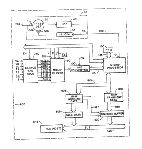
lS IV. The Preferred Embotiment Of The Inv~ntion
A preferred embodiment of the power monitor of
the invention is shown in block diagram form in FIG.
ll as power monitor 800. E~cept for the following
modifications, power monitor 800 is substantially
similar to power monitor 10 of FIG. 1 with like
elements being indicated by like numbers. In power
monitor 800 an int~gr~l numb~r of samples are taken
per cycle of the line input signal FL during an
obsorvstion window which is select~d to b~ 8 cycles
lon~ for purpos~s of example. In this particular
example, the divisors of divider circuits 50 and 60
are s~l~cted such that 16 sample s~ts are taken per
cycl~ of the FL signal ov~r every 8 cycles of the FL
signal. That is, an ensemble of data i~cludes 128
sample sets collected ov~r the ~ cycles of the
ensemble, 16 sample sets bein~ collected during each
30-CF-1010
- 33 - ~ 3 ~
cycle of thQ FL signal. In this embodiment, the
samplin~ times of the 16 sampls sets per cycle are
timed to be distributed substantially uniformly
throu~hout each cycle of the observation window.
Those skilled in the art will appreciat~ that other
observation windows of ~reater or lesser duration than
8 cycles may b~ employed as well in accordanoe with
th~ invention.
As in power monitor 10, the output of A/D
converter 100 is coupled to microproces-Sor llO such
that digital representations of th~ data from each
cycle are supplied to microprocessor 110 which
coordinates the storago of such data in memory. In
this embodiment of the invention, microprocessor 110
lS is coupled to a ~working data~ RAM 805 and a
"transient data~ RAM 810 via a connecting bus 815.
In actual practice, RAM 805 and RAM 810 may be
part of the sama memory chip by using differ2nt
s~artin~ addresses in that memory for the "working
data~ and the "transient data". RAM 805 and RAM 810
will also be referred to as the working data buffer
and the transient data buffer, r~sp~ctively. Working
data buffer 805 and transient data buff~r 810 are of
the first in - first out typ~ and each have sufficient
capacity to hold an entir~ ensemble of data therein,
that is, 128 sample s0ts over ~ cycle~. For example,
1792 bytes was found to be a sufficient size for
workin~ data buffer 805 and transient data buffer 8lO
althou~h this should not be taken a~ bein~ in any way
limitin~.
Th~ nature of the working data and transient data
will be discussed in more detail subs~quently.
However, for now it is noted that th~ working data
30~CF-1010
~ 3~ ~ ~3~8~
buffer 805 and transienk data buffer 810 are couplad
to the input of a transmit buffer 820 via data busses
825 and 830. Transmit buffer ~20 exhibits the same
size as buffers 805 and 810. Transmit buffer 820 is
coupled via a connecting bus 835 to a host bus 840 to
which a programmable lo~ic controller (PLC) 845 or
other host is coupl~d. Host 8~5 requests working
data, transient data and calculated data from power
monitor 800 as will b~ se~n subsequ~ntIy. For exampl~
a programmable lo~ic controller may be employed as PLC
or host 845. The communication bus within such
controll~r may be conveniently employ~d as host bus
~40.
Although 128 sampl~ sets ar~ collected in a
sequential manner over the 8 cycles of a particu1ar
ensemble, the 128 samples sets are stsred in working
tata buffer 805 in an intarlea~ed manner. More
specifically, the 1~8 samples sets of an 8 cycle
ensemble ar~ taken sequentially in the order shown in
the leftmost column of FIG. 12 startin~ with sample
set 1 of cycle l ~SSl). It will be racall~d that each
sample actually includos a samples taken
simultanoously, namoly VA, VB, VC, IA, IB and IC (plus
IN and spare S). Sampling o~ th~ first cycl~
continu~s with the taking of samplo s~ts SS2-SSl6.
Then, sampling of the second cycle comm~nces with
sample set SS17 and continues through sampl~ set SS32.
In a like mann~r, sampling of th~ third cycle
commences with the taking of samplo s~t SS33 and
continues throu~h SS48. Samplin~ continues in the
same fashion with remaininB cycles 4-8 until ~ll 12B
cycles of the ensemble are coll~cted.
30-GF-1010
~ 3 1 ~
As mentioned above, althou~h sample sets SS1-
SS128 are collected sequentially, these samples are
not stored in memory in the order col lected but rather
are stored in the interleaved fa~hion shown in the
S cen~er ~olumn of FIG. ~2. In this manner ei~ht cycles
of data ar~ formed into the ~quivalent OI a ~in~,le
cycl~ of data prior to watts, vars and power factor
processin~ by microprocessor 100. In more detail,
the leftmost column of FIG. 12 represents the sampl in~
order of the sample sets SS1-SS128 and the rightmost
column represents th~ interleaved storage order in
Wor~iA~ data memory ~05 of sampl~ sets SSl-SS128. To
achieve such interleavin~, as the data is ta~en,
sample set SS1 is stored in memory location 1, SS2 is
stored in location 9, SS3 is stored in location 17 and
so forth for the remainder of the data of the first
cycle as shown in FIG. 12. When the first sample set
of the second cycle, namely SS17, is taken, SSl7 is
interleaved back into the alreaty stored data by
storing SS17 in memory location 2 which is i~mediately
subsequent to memory location 1 used for the first
cycle. Sample set SS18 is stored in memory location
10 which is immediately ~ubs~quent to memory location
~ used for the first cyclo. In summary, th~ storage
locations of the 16 sample sets of the second cycle
are advanced on~ forward with r~spect to the storage
locations of th~ sample sats of the first cycle.
Continuin~ in the same fashion, tho stora~e locations
of the 16 sample sets of the third cycle are advanced
one forward with respect to the storage locations of
the sample sets of tho second cycle and so forth until
all 8 cycles of data SSl-SS128 are interleaved to form
the equivalent of a single conden-~ed cycle of volta~e
.
30~GF-1010
- 36 - ~31~
and current data. Thus the working data buffer 805 is
filled with an interleaved ensemble of SSl-SS1~8 data
in th~ above described manner to simulate a sin~le
cycle of the observed line si~nal.
After the ensemble of working data is collected
in working data buffer 805, microprocessor 110
processes the working data to determine tho real power
~watts), ima~inary power (vars) and power assoc;ated
with the data in the ensembl~. In this particular
embodiment of the invention, the watt~, vars and p~w~r
factoi are stored in th~ calculated data Icalc data)
buffer 850 which is coupled to wonking data buffer 805
as shown in FIG. 11. The calc data buffer B59 is
coupled to bus 840 such that the calculated data can
b~ provided to bus 840 and PLC 845 approximately once
per second. The calculated data i~ automatically sent
to PLC 845 approximately once per s~cond without PLC
or host 845 requestin~ such calculatet data.
An example of one voltage and current sensing
circuit which may be employed in conjunction with the
power monitor of the present invenkion i.s shown in
FIG. 13 as sensing circuit 855. Sensing circuit 8~5
is of the lina to n2utral typ~ although a line to line
type sensing circuit could be employ~d as well. FIG.
13 shows three phases of power as phases A, B and C
and a neutral lin~ designated N. In s~nsing circuit
855, tho lin~ to neutral voltages ar~ sensed and
designated VA, VB, VC as shown. The currents in the
resp~ctive phases A, B and C are sensed and are
desi~nated IA. IB and IC, respectively. as shown. The
current in th~ neutral lin~ i5 desiBnated IN.
30-~F-1010
- 37 -
~ 3~4~
More specifically A transformer 860 is coupled to
lin~ N to sense the current IN ther0in as shown in
FIG. 13. Current ~ransformer ~CT) windings 865A, 865B
and 865C are inductively coupled to phases A, B and C
as shown. Each of windings 865A, 865B and 865C
includes opposed ends desi8nated 1 and 2 combined with
the windin~ number. Ends 86~A1, ~65B1 and 865C1 are
coupled together and to ground as shown in FIC. 13.
Additionally, ends 865A1, 865B1 and a65c1 ~re coupled
via conductors 870A, 870B and 870C to ends 865A2,
865B2 and 865C2, respectively. Currsnt transformer
windin4s 875A. 875B and 875C ar~ inductively coupled
to conductors 870A, B70B and 870C such that the
voltag~ induced in each of wintings 875A, 875B and
875C i s i nd i cat i v~ of th~ currents IA, IB and IC
flowing throu~h phases A. B and C respectively.
Sensing circuit 855 includes potential
transformer (PT) windings 880A, 880B and 880C. One
end of each of potential transformer windings 880A,
880B and a80c are electrically coupled to phases A,
and C as shown in FIC. 13. The load associated with
phases A, ~ and C is coupled betw~n n~utral N and
node ~85. The remainin~ ends of each windings 880A,
880B and 880C are coupled to~eth~r at nod~ 885.
Potential transformer windin~s 890A, 8908 and 890C are
inductively coupled to windin~s 880A, 880B and 880C
such that phase volta~es VA, VB and VC appear across
windings 890A, 890B and 890C as shown in FIG. 13. One
end of each of windings 890A, 890B and 890C is coupled
to ground. In this manner, sensing circuit 855
provides th~ power monitor with VA, VB, VC, IN, IA, IB
and IC data for processing. This data is used to
determine true RMS volta~e and current alon~ with real
30-GF~lOlO
- 3~ ~
13~8~9
and ima~inary power on a per phase basis. Total
enor~y and system power factor are al~o provided.
Microprocessor llO calculates th~ real power
WATTS, ima~inary power - YARS, and power factor - PF
associated with a particular ensemble as follows:
For line t~ n~utral connected potential transformers
~PT's):
llATTSA = --- ~ VA ( j ) * IA( j )
M J=l
.
1 12~
~ATTSB = ~ VBSj)*IB~j)
M J=
1 128
WATTSC ~ ~ VCtj)*IC~j)
M j~l
TOTAL WATTS 3 ~ATTSA ~ WATTSB + WATTSC
wherein WATTSA, ~ATTSB and WATTS~ ropr~sent the real
power of phas~s A, B and C, rospectivoly ant wherein M
oquals tho number of sampl~ in tho ~n~emble. VA~;),
15 YBt j ) and VC~ j ) repre~;ont tho voltag~ samplas from
line to neutral of th~ respectiv3 phas~ being
calculated and I~ j ) represent the current samples of
tho resp~ctive phas~ beinB calculated. It is noted
that in this embodiment of the invention, for
convenionc~ phase an~le terms in th~ WATTS and VARS
equations are not shown sinc~ phase angl~ information
is included in th~ IA, IB and IC variables. Tho value
of j correspontin~ to th~ volta~o and current samples
stored in m~mory ar~ shown in tha ri~htmost column of
FIG. 12.
30 - GF - 1 0 1 0
1 3 1 ~
1 128
VARSA - --- ~ YA(j)~IA(j ~ 90 de~rees)
M j-l
1 128
VARSB - -- ~ VB(j)~IB(j ~ 90 degrees)
M j=1
1 128
VARS~ = --- ~ VC(j)*IC~j + 90 degr0es)
J~
TOTAL VARS - ~ARSA ~ VARS8 ~ VARSC
wherein VARSA, VARSB and VARSC represent the imaginary
power~ of phases A, ~ and C, respectively. YA~;),
VB(j) and VCtj) still represent th3 volta~e samples
from line to neutral of the r~sp~ctiv0 phases being
calculated, The I(j + 90 degrees) current values are
obtained by retrievin~ the sample which is stored in
memory in a location correspondin~ to 90 de~rees after
the particular I(j) sample. Since the length of the
ensemble (128 sample~ ssts) a~ter ~torage in memory
repres~nts one cycle or 360 d~roos, 90 d~rees
corresponds to 1~3/4 or 32 memory locations. Thus, to
retrieve a current valu~ I(j + 90 de~ree~) wherein j =
1, th~ d~sired current sampl~ at I(1+32) or I(33) i~
actually rotri~ved.
For line to line connected potential transformers
(PT's)
WATTSA = --- ~ IA~j + 90 de~rees)*(VA(j))/(3)1/2
M J=l
30-CF-1010
~ ~0 --
.~ 3 ~ 9
1 128
WATTSB = --- ~ IB(j ~ 90 degrees)*(VB(j))/(3)1/2
M J=1
1 IZ~
WATTSC = --- ~ IC(j + 90 desrees)*(VC(j))/~3)1/~
J-
TOTAL WATTS = WATTSA + WATTSB ~ WATTSC
wherein WATTSA, WATTSB and WATTSC represent the real
power of phases A, ~ and C, respectively. VA~;),
VB~j) and VC~j) in this c se r~present the volta~e
samples from lines ~ to C, C to A, and A to B,
respectively, and I(j) represents the current samples
of the respectiv~ phase b~ing calculated.
1 128
VARSA = --- ~ IA(j)*~VA(j))/~3)1/2
M J=l
1 128
VARS~ (j)*(VBlj))/(3)112
J~
1 128
VARSC = --- ~ IC(j)*~VC(j))/(3)
M j=1
TOTAL VARS = VARSA + VA~S~ + VARS~
POWER FACTOR = TOTAL WATTS
_____________________________
~TOTAL WATT2 + TOTAL VAR2)1/2
In summary, microprocsssor 110 calculates the
parameters expressed above from tho sample information
in workin~ data buffer 805 and sends the calculated
data to th~ Calc Data buffer B50. The calculat~d dat~
30-CF-1010
- 41 - 1 3.~ ~ 8~
is th~n communicated to tha PLC host 8~5 approximately
on~ time per second.
Each current sample I~j) is test~d by
microprocessor 110 to determine if it i5 a transi~nt.
g That ls, each current ample I(j~ i5 com?ared with
predetermined threshold level which if exceeded
indicates that the particular I(j) sampl~ i5 a
transient. In this particular embodiment of the
invention, to assure accuracy in trapping a transient,
a transient is determined to be detected wh~n
microprocessor 110 finds that two successive I(j1
sample~ exhibit an amplitude which 0xcoeds th0
predetermined threshold level. Wh~ther or not a
transaent is found, the same incomin~ data which is
stored in working data buffer 805 in interleaved
fashion is also stored in transient data buffer 810 in
non-interleaved fashion. That is, the sample sets
SSI-SS128 are stored sequentially in transient data
buffer 810 in the same order a~ that in which they
were taken by sample and hold circuit 80.
If it is determined that th~ current cycle
contains a transient, then microprocessor 110
instructs transi~nt data buff~r 810 to retain the data
from the last two protransient cycl~s prior to the
current cycle. Th~ sample data from the current cycle
containin~ the transient is also retained in transient
data buffer 810. Microprocessor 110 also instructs
transient data buffer 810 to stor~ the sample data
from the 5 post-transient cycle~ occurrin~ after the
cycle found to contain th~ transient. In this manner.
after a transient is detect~d, transient data buffer
B10 is filled with 8 cycles of sample data or 128
samples sets stored in non-interleaved fashion. When
30-GF-1010
13~ 5~9
microprocessor llO finds that a transient has
occurred, PLC host 845 is so notified.
If PLC ho~t 845 makes no request for the
transient data contained in transient data buffer 810,
then the sample data from subsequent cycles are
permitted to overwrit~ whatever data is stored in
transient data buffer 810. However, if PLC host 845
should make a request for the transient data in
transient data buffer 810, then the contents of
transient data buffer 810 are sent to transmit buffer
83S. The transient data is transmitted from transmit
buffe~ 820 in bursts to PLC host 845 via busses 835
and 840.
In actual practice, to avoid unnecessarily moving
data from buffer to buffer. transmit buffer a20,
transient data buffer 810 and working data buffer 805
are all the same size and aro part of the same memory.
Each of buffers 820, 810 and 805 is assi~ned a
startin~ address or location by microprocessor 110.
Thus, should microprocessor need to send the transient
data within transient data buffer 810 to transmit
buffer 820, th~n microprocessor 110 redefines the
transient data buffer 810 to bo th~ transmit buff~
8Z0 and vice versa. That i5, microprocessor 110 now
consider~ the starting address of the transient data
buffer 810 to be the startin~ address of transmit
buffer 820. The transient tata within transmit buffer
820 is then transmitted in bursts to PLC host 845.
In a similar manner.. should PLC host 845 request
that microprocessor llO send host 845 the i~terleaved
workin~ data contained in working data buff~r 805,
then rather than actually sendin~ the workin~ data to
transmit buffer 820 (although this still may be done),
l 30-GF-lolo
~3 ~ ~ 3 ~
microprocessor 110 redefines working data buffer 805
to be transmit buffer 820 ant vice versa. More
specifically, microprocessor 110 now considers the
startin~ address of th~ workin~ data buffer 805 to be
the starting addrsss of transmit buffer a20. The
contents of transmit buffer 820 ar~ then sRnt in
bursts to PLC host 845.
V. Flowchart
~IG. 14 is a flow chart showin~ a ~eneralized
control program for microproo~ssor 110. The flow
chart of FIG. 14 also summarizes th~ st~ps in the
process of monitorin~ power of th~ present inv~ntion.
A data ensemble of 128 sampl~ sets SS1-SS128 each
including voltaKe and current samples is collected
ov~r 8 cycles as per block 900. As the current
samples of the ensemble ar~ collect~d. each sample is
tested to determin~ if it is a transient as per block
905. Ea~h ensemble of data is stor~d in transient
buffer 810 as per block 910. That is, if the
transient test shows that two successiv~ current
samples (for exampl~, a curr~nt sample in set SS21 ~nd
SS22) e~ceed a predetermined amplitudQ, then a
transient is determined to exist. Under these
conditions, the data from the current cycle as well as
the two pre-transient cycles is kept in transient
buffer 810. Sample set data from the next 5 post-
transient cycles is also stored in transient buffer
310 in non-interleaved fashion to form a complete
ensemble of 128 sample sets.
The data from 0ach ensembl~ is also stored in
working data buffer 805 in interleaved fashion as p~r
30-GF-1010
_ ~4 - ~31~
block 915 in th~ manner described above. If the host
PLC 845 is found to have requested the transient data
from transient buffer 810 at decision block 920, then
th~ contents of transient buffer 810 are placed in
s transmit huffer 820 an block 925. I'he transient data
is sent from transmit buffer 820 to host PL~ 845 at
block 930. However, if the host PLC 845 is not found
to ha~ requested transient data at decision block
920, then flow continues to decision block 935. If
host PLC 845 is found to have requested the working
data f rom work i ng data buffer 805 in decision block
935~ then the working data from buffer 805 is providod
to transmit buffer 820 as per block 940. The working
data is sent from transmit buffer 820 to PLC host 845
in block 945. However, if host PLC 845 is not found
to have requested the work;ng data at decision block
935, then flow continues to calculation block 950.
At block 950 th~ ~ATTS, VARS and PO~ER FACTOR are
calculated by microprocessor 110 from the interleaved
wor~ing data in workin~ data buffer 805 in the manner
already described. The calculated data is sent to
host PLC 845 approximately onc~ p0r second as per
block 955, Flow thon continu~ back to block 900 and
th~ process of collectin~ the n~xt onsemble of data
commences. From the above description it is clear
that as well as provitin~ power monitorin8 apparatus,
tho invention involves a m~thod for monitoring the
pow~r associated with a signal. In ono embodiment the
m~thod includ~s the the steps of sampling the si~nal
turin~ an observation window including a plurality of
cycles of th~ signal to generat~ a plurality of
voltage-current sample sets during each cycle of the
signal, and timing the samplinB Of the signal such
30-CF- 1 0 1 0
131~8A9
that the sample sets are Benerated at d i f f erent
relative time positions from cycle to cycle with
respect to the be8innin~ of each cycle of the
observation window. The method further includes the
S step of determining from the samples sets th~ real and
ima~inary power associated with the si~nal.
In another embodiment, a method is provided for
monitoring power associated with a periodic si~nal
during an observation window including a plurality of
cycles of the si~nal. That method includes the step
of takin~ voltag~ and current samp 1 es dur i n~ f a rst
and s.econd observ~tion windows of the signal to
Benerate a plurality of volta~-current sample s~ts
per cycle of the f irst and second obs~rvation window,
and the step of storing the voltage-current sample
sets taker. during the first observation window in a
f irst memory area. Tho m~thod furthor includes the
step ofanalyzing th~ samples in th~ first memory area
to d~termine the power associated therewith while
during th~ second ob ervation window storing volta~e-
current samples taken during the second observation
window in a second momory area. The method includes
the step of datermining if any of th~ voltaga-current
samples s~t~ represent transients in the si~nal and
the step of desi~nating one of the first and second
memory areaæ as a transient memory area when transient
data is det~rmined to be stored therein. The method
further includes storing in a third memory area the
sample sets occurrin~ in a n~xt observation window
subs~quent to an observation window durin~ which a
transient wa~ determined to have occurred. The also
m~thod includes the step of preventing us~ of one of
the first and second memory areas tesignated as the
30 CP-l~lO
- 46 -
~31~8~
transient m~mory area until the transient data th~rein
is analyzed.
In a preferred ernbodiment, a method for
monitoring th~ power of a substartially periodic
signal is provided including th~ step sampl inB the
signal during an observation window including
plurality of cycles of the si~nal to generate a
plurality of voltage-current sample sets. Each sampl~
set contains at least one volta~e sample and at least
on~ current sample taken substantially at the same
time. Th~ m~thod further include3 th~ st~p of timin8
th~ samplin8 of ths signal such th~t th~ voltag~-
current sample sets are distributed throughout each
cycle of the obserYation window. Th~ m0thod also
inclutes the step of storing in interleav~d fashion in
a first memory area tha sample sets occurrin~ durin~ a
particular observation window so a~ to simulat~ a
single cycle of data in th~ first memory area, and the
step of storing in sequential fashion in a second
momory area th~ sampl~ sets occurrin~ during the
particular observation window.
Th~ foregoin~ describes a power monitor and a
method for monitorin~ power which ar0 capable of
determinin~ the UATTS ~real power) and VARS (volt-amps
reactive or imag;nary power) associated with a
particular power line. The power monitor includes
data acquisition circuitry uniquely configured such
that tho speed requirem~nt thereof is relatively low.
Tha power monitor collects a data base of wav~form
3Q information for th~ purpose of conductin~ waveform
analysis an~ permittin~ transient analysis/display of
transient data. The power monitor provides true RMS
30-~F-lolo
~L 3 ~
voltage and current on a per phase basis and system
power factor and total energy on a system basis.
While only certain preferred feature~ of the
invention have been shown by way of illustration, ~any
modifications and changes will occur to those skilled
in the art. It is to be understood that the present
claims are intended to cover all such modifications
and changes which falI within the true spirit of the
invention.