Note: Descriptions are shown in the official language in which they were submitted.
M~CROW~VE CONNECTOR
Field of the nvention
The present invention is directed to a connector
for microwave transmission lines which provides improved
mechanical stability and cable-to-connector retention
strength while not significan~ly altering the electrical
path of the transmission line.
Backqround of the Invention
Microwave transmission lines themselves are well
known and often take the form of a flexible or semirigid
coaxial cable. Such cables are typically provided with a
connector at at least one end of the cable for connecting
the cable to a source of microwave energy or to a load.
Connectors for microwave transmission lines in the form of
coaxial cables are disclosed in, for example, U.S. Patents
3,778,535 and 4,545,637. Connectors for coaxial cables for
non-microwave uses are disclosed in Patents 3~275J737
4,053,200 and 4,156,554.
It is also known that there are several important
requirements that a microwave connector must satisfy. The
connector must present a constant characteristic impedance,
must have controlled compensation of electrical discon-
tinuities resulting from unavoidable dimensional changes,
must meet close mechanical dimensional tolerances ( i 0.001
inch), and must not introduce reflections in the microwave
transmission line. It is also desirable that the connector
provide high cable-to-connector retention strength, so that
the connector does not introduce a weak mechanical link in
4205-58 -l~
.
~3~85~
the microwave transmission line. The connector must
further provide electrical continuity with minimum ohmic
losses and protect the transmission line from environmental
effects.
Summar~ of the Invention
The present invention provides a connector for
microwave transmission lines which meets all of the cha-
racteristics required of a microwave connector and, in
addition, provides excellent cable-to-connector retention
strength without significantly altering the electrical path
of the transmission line. The present invention provides a
cable-to-connector retention strength on the order of 100%
of the tensile strength of the coaxial cable to which the
connector is attached, in co~trast to prior connectors
which offer cable-to-connector retention strengths only
about half as great.
The present invention is a connector for microwave
transmission lines which have an inner conductor, a low-
density polytetrafluoroethylene dielectric layer surround-
ing the inner conductor, a thin outer conductor surrounding
the dielectric layer, a woven wire braid shield surrounding
the thin outer conductor and an exterior insula-ting cover-
ing surrounding the shield. The connector comprises a
contact ring surrounding and in physical and electrical
contact on an interior surface of the ring with the Quter
conductor. A first end of the contact ring, the outer
conductor and the dielectric layer all terminate in a
common plane. The contact ring has a second end spaced
from the first end of the contact ring. The contact ring
has a shouldered portion between the first and second ends
thereof for contacting the shield and causing the shield to
terminate in a plane parallel to and spaced apart from the
common plane of the first end of the contact ring, the thin
outer conductor and the dielectric layer. A clamp nut
movably surrounds the shield and contact ring along at
least a portion thereof, and a connector shell is provided
4205-58 -2-
~31~
which is removably engageable with the clamp nut and sur-
rounds at least the shouldered portion of the contact ring.
The connector shell has an extending portion adapted to
receive a coupling nut. The outer conductor, the contact
ring, the shield, the clamp nut and the connector shell are
all in physical contact to provide an electrical path from
the thin outer conductor to the connector shell while
keeping a constant characteristic cable impedance.
Descript;on of the Drawin~s
For the purpose of illustrating the invention,
there is shown in the drawings a form which is presently
preferred; it being understood, however, that this in-
vention is not limited to the precise arrangements and
instrumentalities shown. ~
Figure 1 illustrates in simplified form a microwave
transmission line in the form of a coaxial cable fitted at
each end with connectors according to the present inven-
tion. ~`
Figure 2 is a partially-exploded view of a connec-
tor according to the present invention showing the connec-
tor shell removed from the clamp nut.
Figure 3 is a longitudinal sectional view of a
portion of the cable and the connector taken along the
lines 3-3 of Figure 1.
Figures 4, 5 and 6 are transverse sectional v~ews
of the cable and connector taken along the lines 4-4, 5-5
and 6-6, respectively, of Figure 3.
Figure 7 is a longitudinal sectional view of a
portion of a microwave transmission line in the form of a
coaxial cable fitted at one end with a connector according
to an alternate embodiment of the present invention.
Figure 8 is a longitudinal sectional view of a
portion of a microwave transmission line in the form of a
coaxial cable fitted at one end with a connector according
to a third embodiment of the present invention.
4205-58 -3-
1 3 ~
Description o~ the Invention
ReEerring now to the drawings, wherein like numer-
als indicate like elernents, there is shown a microwave
transmission line in the form of a coaxial cable 10 fitted
at each end with a connector 12 according to the present
invention. Connector 12 includes a coupling nut 14, shown
exploded from connector 12 in Figure 1, which is rotatably
attached to connector 12 to enable connector 12 to be
attached to a source of microwave energ~ or to a load.
Coupling nut 14 may be optionally configured as either
male or female to mate with a corresponding female or male,
respectively, connector on the source or load. Coupling
nut 14 may thus be any desired configuration suitable for
attaching cable 10 to a source~or load, and the particular
configuration of coupling nut 14 is not critical to the
invention~
The major elements of connector 12 are shown in
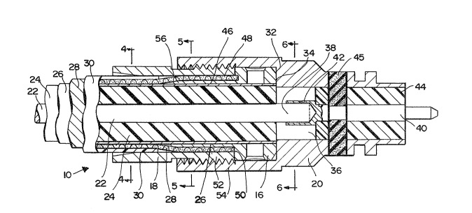
Figure 2. Connector 12 comprises a:`contact ring 16, a
clamp n~t 18 and a connector shell 20, shown exploded from
clamp nut lg in Figure 2.
Connector 12 is best understood by reference to
Figures 3-6. As shown in those figures, cable 10 com-
prises, viewed from the inside out, an inner conductor 22,
a dielectric layer 24 concentrically surrounding inner
conductor 22, a thin outer conductor 26 concentrically
surrounding the dielectric layer 24, a woven wire brai~d
shield 28 concentrically surrounding the thin outer conduc-
tor 26, and an exterior insulating covering 30 concentric-
ally surrounding the shield and forming an outer jacket for
cable 10.
Outer conductor 26 is preferably, but not neces-
sarily, in the form of a thin conductive ribbon wound
spirally with about 40% overlap around dielectric layer 24.
As those skilled in the art will understand, inner
conductor 22 and thin outer conductor 26 form the primary
electrical path for microwave energy being carried by cable
4205-58 -~-
~3~$~6
lo. Typically, -the center conductor is considered to be
the "signal~ conductor and the thin outer conductor is con-
sidered to be the return, or groun~, and acts as an RF
(radio frequency) shield. Wire braid 28 is not the RF
shield, but acts only as a backup for the thin outer
conductor.
Contact ring 16 is provided with a central bore and
concentrically surrounds thin outer conductor 26. The
interior surface of the bore in contact ring 16 is in close
physical and electrical contact with outer conductor 26 and
permits a near-perfect transmission line to be maintained
in the area of contact between the outer conductor 26 and
the interior surface of the bore in contact ring 16. A
first end 32 of contact ring l'~,abuts an interior shoulder
34 on connector shell 20. As can be seen from the figures,
connector shell 20 has a larger diameter interior bore to
surround contact ring 16 and clamp nut 18, and a reduced
diameter bore 36. Shoulder 34 is forme,d between the larger
diameter bore and reduced diameter bore 36. Thin outer
conductor 26 also abuts shoulder 34 of connector shell 20.
Thus, first end 32 of contact ring 16, outer conductor 26
and dielectric layer 24 all terminate in a common plane
defined by shoulder 34. An end 38 of inner conductor 22
proiects beyond the common plane defined by shoulder 34 of
connector shell 20. End 38 of inner conductor 3~ is
received in a pin 40. Pin 40 is substantially coaxial witk
inner conductor 22 and extends within reduced bore 36 and
beyond the end of connector shell 200 A dielectric plug 44
concentrically surrounds pin 40 and supports pin 40 while
insulating it from connector shell 20.
Although dielectric layer 24 may be any suitable
dielectric, it has been observed that the loss characteris-
tics of the cable are improved when the dielectric layer 24
is made of an extruded low-density polytetrafluoroethylene
(PTFE), also known by its trademark "TEFLON." The dielec-
tric constant of solid PTFE ranges from 2.0 to 2.1; "low
4205-58 -5-
8 ~ ~
density" PTFE is defined as haviny a specific gravi~y less
than 2Ø The loss tangent for a cable made with solid
PTFE, for instance, has been observed to be .0002; for low-
density PTFE, .00006~. Clearly, low-density PTFE is very
desirable for its electrical properties. However, low-
density PTFE does not have the mechanical rigidity of solid
PTFE. It has been found that when low-density PTFE is used
as a dielectric, flexing forces on pin 40, due to engaging
and disengaging connector 12, will cause pin 40 to recede
into the cable or pull out from the cable.
To prevent this axial motion of pin 40 or center
conductor 22, pin 40 and plug 44 are retained in place, or
~captivated", by epoxy 45 in known manner (see, e.g., U.S.
Patent 3,292,117). Epoxy 45 e~gages two oppositely-facing
shoulders created by a reduced diameter portion of pin 40.
In the embodiments shown in Figures 3-7, a second
end 46 of contact ring 16 extends for a distance betweer.
outer conductor 26 and wire braid shie~d 28 so that shield
28 surrounds the second end 46 of contact ring 16. Shield
28 is preferably joined to second end 46 by soldering, such
as at 48. Contact ring 16 is provided with a shoulder 50
against which the end of shield 28 abuts. Shoulder 50
defines a plane parallel to the plane of shoulder 34 on
connector shell 20 and spaced apart from it. Thus, shield
28 does not terminate in the plane of the first end 3~ of
contact ring 16 and the ends of outer conductor 26 and~
dielectric layer 24, but terminates a distance behind it.
Clamp nut 18 movably surrounds a portion of cable
10 and is in physical and electrical contact with at least
that portion of shield 28 which surrounds the second end 46
of contact ring 16. Clamp nut 18 is free to rotate with
respect to cable 10 and has an externally threaded portion
52 which engages an internally threaded portion 54 of the
larger-diameter bore in connector shell 20. When connector
shell 20 is threadably engaged with clamp nut 18, there is
4205-58 -6-
.
~ 31~8~;~
a direct electrical path from outer conductor,26 to connec-
tor shell 20.
Second end 46 of contact ring 16 is provided wikh a
slight chamfer 56 to allow a smooth transition of shield 28
over second end 46~ Second end 46 of contact ring 16
provides improved mechanical stability to connector 12
while not disturbing the electrical path of the transmis-
sion line. That is, uniform spacing between inner conduc-
tor 22 and outer conductor 26 is maintained in the contact
area. In addition, by placing the second end 46 of contact
ring 16 between the outer conductor 26 and wire shield 28,
more surface area of the wire braid 28 can be soldered to
second end 46, providing superior mechanical stability
between the outer conductor 2~ and wire braid 28. The
result is a mechanical robustness not found in prior
connectors. The present invention allows for a connector-
to-cable retention force of at least 100~ of the cable
tensile strength, as compared to only ~5~0% in prior connec-
tors. Moreover, terminating wire braid 28 behind the
plane of the first end of the contact ring, outer conductor
26 and dielectric layer 24 facilitates machining the end of
cable 10 to a smooth surface. With the structure of the
present invention, the possibility of the hraid wires of
shield 28 "smearing" over dielectric layer 24 and the
resultant likelihood of voids being created between~the
braid wire is eliminated. This results in a connector with
highly consistent electrical characteristics.
A slightly different embodiment of the connector of
the present invention is illustrated in Figure 7. The
embodiment shown in Figure 7 is the same as the embodiment
already described, with the exception of the dielectric
plug in connector shell 20 and the pin contact. Instead
of the contact receiving an extending end of the center
conductor 22, conductor 22 terminates in the common plane
of conductor 26, dielectric layer 24 and first end 32 of
contact ring 16, and is provided with a socket 58 to
4205-58 -7-
~ 3 ~
receive a shouldered projection 60 on pin contact 62.
Projection 60 is preferably soldered in place in socket 58.
As seen in Figure 7, projection 60 has a slight shoulder 6~
which abuts the end of center conductor 22. Diel~ctric
plug 44 surrounds and supports pin 62 and abuts dielectric
layer 24 of cable lo. In this embodiment there is only a
single step, at shoulder 64, from the diameter of conductor
22 to the diameter of pin 62, which allows connector 12 to
e~en more closely approach a reflectionless termination.
The embodiment shown in Figure 8 shows another
arrangement of the concentric layers around the conductor
22. It has been found that the loss characteristics
through the connector are improved when the shielding braid
28 around the outer conductor ~6 terminates at a distance
from the plane at which the outer conductor 26 and the
dielectric 24 terminate. To allow this arrangement of
parts, contact ring 72 fits into clamp nut 18, as with the
previous embodiments. However, in embodiment of Figure 8,
contact ring 72 is provided with an axial bore having
three different diameter portions on the interior surface
of the bore. In the first portion, the diameter of the
bore is large enough to receive the entire diameter of
cable 10. The next diameter portion is large enough to
receive only that part of the cable including wire braid 28
but excluding outer jacket 30. These two diameter porbions
define an interior shoulder 72a, against which jacket 3Q
abuts. The last diameter portion is only large enough to
receive the part of the cable comprising center conductor
22, dielectric 24 and outer conductor 26. The second and
last diameter portions define a second shoulder, 72b,
against which braid 28 abuts. Shoulder 72b ensures that
braid 28 will terminate a distance from the common plane of
center conductor 22, dielectric 24 and outer conductor 26,
while allowing the radial distance between center conductor
22 and outer conductor 26 to remain constant all the way to
the common plane.
4205-58 -8-
-` ~31~
The embodiment of Figure 8 also shows another
ncaptivation" techni~ue, which may be used with -the embodi-
ments of Figures 3 or 7 as well. In this embodiment pin 80
is soldered through opening 82 to the conductor 22. Pin 80
is shaped with a reduced diameter section to form two
opposite facing shoulders which are embedded in captivating
assembly 74, 76, 78. The shoulders of pin 80 are held by
epoxy 74, which thus prevents any axial motion of pin 80 or
conductor 22 relative to the connector.
Although the particular captivating assembly 74,
76, 78 is shown in Figure 8 in conjunction with the contact
ring 72, the captivating means of Figure 8 may be used with
the contact ring 16 of Figures 3 or 7. Conversely, cap-
tivating means 45 shown in Fig~res 3 or 7 may be used in
conjunction with contact ring 72 shown in Figure 8.
The present invention may be embodied in other
specific forms without departing from the spirit or
essential attributes thereof and, ac~ordingly, reference
should be made to the appended claims, rather than to the
foregoing specifications, as indicating the scope of the
invention.
4205-58 -g-