Note: Descriptions are shown in the official language in which they were submitted.
~ 13~8~
IMAGE PROCESSING SYSTEM
BACKGROUND OF THE INVENTION
1. Field of the Invention
~ he present invention relates to an image
processing sys~em enabling clear reproduction of an
original document including mixed characters, ruled
lines, and photos. The characters, ruled lines t and
photos in the original document are scanned by an image
scanner and a scanned image is converted to a multi-
level signal and further converted to a binary signal.
1~ The original document is clearly reproduced based on
processing of the binary signal according to the present
invention.
2. Description of the Related Art
Image processing systems are widely used in
the field of inormation processing systems. In image
processing, a character can be easily converted to a
binary signal based on a predetermined threshold level
because the contrast of light and shade thereof is very
clear. That is, for example, when the character portion
(black portion) is a value "1", ~he remaining portion
(white portion) is a value "0". Accordingly, when all
areas of the document comprise only characters, the
image processing of the original document is very easy.
When characters, ruled lines, and photos are
mixed on one sheet of the original document, the image
processing thereof is very troublesome because the
photos contain half-tone colors such as gray colors so
that the multi-level signal includes gray color areas,
and fine lines of characters or ruled lines also become
grày.
One known method for processing half-tone
colors is called "dithering". In the dither method, the
light and shade level of each pixel o~ the original
image are compared with a plurality of threshold levels
(variab]e threshold level), and ON/OFF of the display
,~
- 2 - ' 131~885
elements are determined based on the resultant data after com-
parison. In this case, each of threshold levels is selected at
random at every pixel by using, for example, a table o~ random
numbers.
Japanese Unexamined Patent Puhlication (Kokai) No. 58-3374
discloses a method for processing a half-tone color based on the
density level of the black pixel. That is, this method includes
steps for dividing the original image into a plurality of blocks,
and for obtaining the difference between a maximum density level
and a minimum density level in each block. When the difference
value is larger than a predetermined threshold level, the area
of such a block is binary-coded by a constant threshold level as
a binary image area. When the difference value is smaller than
a predetermined threshold level, this area is binary-coded by
dithering as a half-tone area.
Japanese Unexamined Patent Publication (Kokai) No. 60-196068
discloses a method for determining either the binary image area
or the half-tone area. This method incudes the steps for binary-
coding of the scanned data based on a plurality of threshold
levels, for counting the number of values "0" and "1" in each
threshold level, for comparing the counted numbers with each
threshold level, and for detecting a change of the counted
numbers by comparing them with a previous number. Whether the
binary image area or the half-tone image area is to be selected
is determined from this change of the counted mlmbers.
SUMMARY OF THB INVENTION
A feature of one embodiment of the present invention is to
provide an image processing system enabling clear reproduction
of an original document including mixed characters, ruled lines,
~0 and photos.
In accordance with an embodiment of the present invention
there is provided an image processing system for obtaining a
binary signal from a multi-level signal read by an image scanner
from an original document including mixed characters, ruled
lines, and photos, and then obtaining a reproduced image from the
binary signal, the image processing system comprising: fixed
slice processing means for receiving the multi-level signal, for
s~:
3 - ~3~8~
slicing the multi-level signal by a pre~etermined fixed -thres-
hold, and for outputting the binary siynal sliced by the fixed
threshold level; half-tone processing means for receiving the
multi-level signal, for slicing the multi-level siynal by a
plurality of threshold levels defined by a dither method, and for
outputting the binary signal sliced by the plurality of threshold
levels defined by the dither method; charac~er/photo separating
means for receiving the multi-level signal, for detecting a
pattern of the multi~level signal, for separating either a
character portion or a photo portion based on the pattern and for
outputting a selection signal, the character/photo separating
means comprises a successive gray color detection circuit for
receiving the multi-level signal, and for obtaining binary
signals after slicing the multi-level signal based on the fixed
threshold level, and detecting a number of the binary signals
occurring in succession within one line of the binary signal; and
a fine line detection circuit for receiving the multi-level
signal, and for detecting a change of density level of the multi-
levels signal between adjacent lines; and selection means for
selecting either the fixed slice processing means or the half-
tone processing means based on the selection signal from the
character/photo separating means.
BRIEF DESCRIPTION OF THE DRAWINGS
In the drawings:
Fig. 1 is a schematic block diagram of a general image
processing system;
Fig. 2 is a schematic block diagram of a conventional image
processing system;
Fig. 3A is a view for explaining an original document
including characters, photos, and ruled lines;
Fig. 3B is a view for explaining a multi-level slgnal
including characters and photos;
Fig. 4 is a schematic block diagram of an image processing
system according to the present invention;
Figs. 5A, 5B and 5C are views for explaining a slicing state
of a multi-level signal including characters and photos;
Fig. 6 is a schematic block diagram of a fine line
~ 3 ~
detection circuit according to the present invention;
Fig. 7 is a schematic block diagram of a successivP
gray color detection circuit according to the present
invention;
~ig. 8 is a schematic block diagram of an image
processing system according to one embodiment of the
present invention;
Fig. 9 is a schematic block diagram of an image
processing system according to another embodiment of the
present invention;
Figs. 10A, 10B and 10C are views for explaining
slicing state of a multi-level signal including ruled
lines, photos, thick characters, and fine line charac-
ters; and
Fig. 11 is one embodiment of a successive black
color detection circuit in Fig. 9.
DESCRIPTION OF THE PREFERRED EMBODIMENTS
Before describing the preferred embodiments,
problems in a conventional method are explained below in
detail.
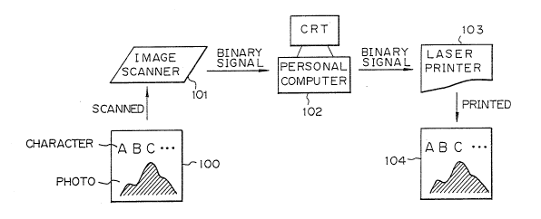
Figure 1 is a schematic block diagram of a general
image processing system. In Fig. 1, reference num-
ber 100 denotes an original image of a document to be
scanned, 101 an image scanner, 102 a personal computer
with a display (CRT), 103 a laser printer and 104 an
image reproduced by the printer. The original image
includes characters, ruled lines, and photos. They are
scanned by the image scanner 101 and converted to a
multi-level signal and then converted to a binary signal
having values of "0" or "1". The binary signal is input
into the personal computer 102 and printed by the laser
printer 103 so that the original image can be
reproduced.
In this case, the scanned multi-level signal of the
character portions of the original image 100 is binary
coded by the image scanner 101 based on a fixed slice
level method having a step in which the multi-level
1 3 ~
signal is binary coded by the predetermined fi~ed
threshold level. Further, the mulki-level signal of the
photo portions of the original image is binary-coded by
the half-kone processing method based on dithering for
binary coding the multi-level signal based on a prede-
termined dither pattern.
As explained above, the character and the photo
portions are sepaxately binar~-coded by using the fixed
slice level method and the half-tone processing method
(dithering). This reason is explained as follows. That
is, when both characters and photo are simultaneously
binary-coded by the predetermined fixed threshold level,
the photo portions cannot be clearly reproduced since
the photo portions contain half-tone colors. In con-
trast, when both characters and photos are simulta-
neously binary-coded by dithering, the character
portions cannot be clearly reproduced since the
character portions comprise only two colors such as
black and white colors.
In general, the photo portion has a tone gradation
in half-tone colors. The gradation is expressed by a
concentration of black dots.
Figure 2 is a schematic block diagram of a conven-
tional image processing system. This system is dis-
closed in Japanese Unexamined Patent Publication (Kokai)No. 61-221886. In Fig. 2, reference letter A denotes a
dither processing means, B a multi-level signal pro-
cessing means, C a separation means and D a selection
means. The dither processing means A obtains a dither
value from the multi-gradation data of each pixel of the
image including characters and photos. The multi-level
signal processing means B obtains multi-level data after
comparing the multi-gradation data with at least two
threshold. The separation means C separates each block
of the image in accordance with either the binary image
area or the half-tone image area. The selection means D
selects the dither processing means A or the multi-level
- 6 - ~ 3~
signal processing means B based on the resultant data
from the separation means C.
The conventional system utilizes the characteristic
by which the density gradation of the edge of the
character is sharpened compared with that of the half-
tone. Accordingly, each block of the image is separated
based on the change of the density gradation of the edge
as to whether the binary image area or the half tone
image area is selected.
However, when fine ruled lines are mixed among the
character portions and the photo portions in the
original image, these fine lines are not clearly
reproduced as with the ruled lines in the above conven-
tional system. This problem is explained below in
derail.
Figures 3A is a view for explaining an original
document including characters, photos, and ruled lines.
Figure 3B is a view for explaining the multi-level
signal scanned along an arrow line shown in Fig. 3A. In
Fig. 3A, 110 denotes an original image, and RL a ruled
line. In this case, when the character portions C are
binary-coded by the ~ixed slice level after converting
to the multi-level signal, peak/valley portions thereof
are clearly obtained. However, the ruled line and the
photo portions P becomes unclear when using this fixed
slice level because the multi-leval signal MS of the
photo portion includas gray colors. In contrast, when
the photo portions are binary-coded by dithering, the
character portions become unclear. Further, since the
line width of the ruled line is very fine compared with
that of one scan line of the image scanner, the image
scanner cannot separate the ruled line.
An image processing system according to the present
invention is explained in detail hereinafter.
Figure 4 is a schematic block diagram of an image
processing system according to the present invention.
In Fig.4, reference number 1 denotes a fixed slice level
1 3 ~
7 --
processing circuit, 2 a half-tone processing circuit,
3 a character/photo separation circuit, and 4 a
selection circui-t. Further, FSS denotes a fixed slice
signal HTS denotes a half-tone signal, and MS denotes a
multi-level signal, for example, sixty-four levels
(values) indicating the density gradation of the color
of the image.
In Fig. 4, the multi-level signal ~S is input in
parallel to the circuits 1 to 3. The outputs of the
circuits 1 and 2, i.e., the fixed slice signal FSS and
the hal-tone signal HTS r are input to the circuit 4.
The circuit 3 separates the multi-level signal MS as to
whether the multi-level signal indicates a character
portion or a photo portion. In the selection circuit 4,
when the circuit 3 detects a Gharacter portion, the
fixed slice signal FSS is selected. When the circuit 3
detects a photo portion, the half-tone signal HTS is
selected.
Figures 5A, 5~ and 5C are views for explaining a
slicing state of the multi-level signal including
characters and photos. Reference is a character
portion, and P a photo portion. Further, Tho denotes a
threshold level, and MS the multi-Ievel signal. As
shown in the drawing, the multi-level signal MS includes
the gray colors in the photo portion P, and denotes
clear white and black colors in the character portion C.
When the multi-level signal MS is sliced by the thres-
hold level Tho at which level is set in the neighborhood
of the white level, the resultant data is obtained as
shown in Fig. 5B. In this case, the value "0" is
continued during the term T in the photo portion P, but
"0" and "1" are repeated at every cycle "t" in the
character portion C.
In the present invention, when the number of ''O's'
which occur in succession exceeds a predetermined
reference value "tho", this portion is determined as the
photo portion P so that the half-tone signal HTS of
- 8 - ' ~ 3~
Fig. 4 is selected as the half-tone image portion.
Accordingly, when the number of "0's" does not exceed
the predetermined reference value "tho", this portion is
determined as the character portion so that the fixed
slice signal FSS is selected.
Further, when a character is written by fine lines,
the multi-level signal MS is shown by Fig. 5C (see,
Fig. 10C). In this case, when the multi-level signal MS
is sliced by the threshold level Tho ~ the character
~o portion C is incorrectly determined as the photo portion
if the number of 'l0's'' exceeds the reference value
"tho". Accordingly, a fine line detection circuit is
provided in the system to avoid the above mis-judgement.
Figure 6 is a schematic block diagram of a fine
line detection circuit according to the present
invention. This circuit is included in the charac-
ter/photo separation circuit 3 in Fig. 4. In Fig. 6, M
denotes a multi-level signal holding block, 21 and 22
shift registers, 23, a read only memory (ROM), and 24 a
register group. References X1 to X8 and S0 denote
pixels each constituted by the multi-level signal. S0
is a center pixel of this block. The fine line
detection circuit is constituted by a differential
circuit which detects a change of the light and shade of
~5 adjacent vertical and horizontal pixels relative to the
center pixel. The differential circuit includes a
primary differential circuit (ROM 23) and a secondary
differential circuit (ROM 23'). In these circuits, the
primary differential value Y1 and the secondary differ-
ential value Y2 are given as follows.
Y1 = S0 - 1/4 (X~ + X4 + X6 + X8) (1)
Y2 = 1 X6 ~ X2 1 + I Xg ~ X4 1 (2)
Accordingly, to calculate the above formulas,
first, the multi-level signals X4 , S0 and X8 (line Ln)
are sent to the shift resister 21, and then the multi-
level signals X5 , X6 , and X7 (I.ine Ln+1) are sent to
the shift register 21. ~t the same time, the line Ln
_ 9 _ ~315~
previously stored in -the shift register 21 is shifted to
the shift register 22. Further, the multi-level signals
X1 , X2 and X3 (line Ln-1) are sent directly to the
register group 24. As a result, a 3 x 3 matrix is
obtained in the register group 2~.
Each of the multi-level si~nals X2 , X4 , X6 , X8 ,
and S0 is extracted from the register group 24 and input
to the ROM 23 ~or calculating the formula (1). q'he
ROM 23 has the function that the Yalue "1" is output
therefrom when the primary differential value Y1 is
equal to or larger than a threshold level Yh. Simi-
larly, each of the multi-level signals X2 , X4 , X6 ,
and X8 is extracted from the reyister group 24 and input
to the ROM 23' for calculating the ~ormula (2). The
ROM 23' has the function that the value "1" is output
therefrom when the secondary differential value Y2 is
equal to or larger than a threshold level Yh'.
Figure 7 is schematic block diagram of the succes-
sive gray color detection circuit according to the
~o present invention. This circuit is also included in the
character/photo separation circuit 3 in Fig. 4. This
circuit is used for detecting number of "0's" during the
term T in the photo portion of Fig. SB. In Fi~. 7, 21,
22, and 24 are the same elements as that of Fig. 6.
Each of pixels Xll to X33 correspond to X1 to X8 in
Fig. 6. Reference number 31 denotes a comparator, 32 a
counter, 33 a flip-flop circuit, 34 an AND gate, and 35
an inverter.
First, the threshold level Tho and the multi-level
signal X21 of the center line are input into the com-
parator 31, and the signal X21 is compared with the
threshold level Tho so that the binary signal X21A is
output ~rom the comparator 31. The threshold level Tho
is the same as that of Fig. 5A. The binary signal X21A
is input into the counter 32. the counter 32 is up-
counted when the binary signal X21A is the value "1~.
Further, a reference value LH and a clock signal CLK are
- 10 ~
input into the counter 32. The output "1" of the
counter 32 i6 obtained when the count number thereof is
equal to or larger khan the reference value LH. This
reference value LH is used for separating either the
character or the photo and is previously determined to
be a larger value than the successive number of the
binary signal X21~ at the character portion.
Accordingly, when the multi-level signals are
sequentially input into the comparator 31 in response to
the clock signal CLK of the scanning direction, the
output binary signal X21A becomes "1" in succession when
the phoko portions are scanned. The counter 32 is
up-counted when the value "1" is input. When the count
number of the counter 32 reaches the reference value LH,
the counter 32 outputs the value "1". The value "l"
from the counter 32 is continued while the binary signal
X21A is the value "1". The value "1" is input to the
flip-flop circuit (F/F) 33 and the value "l" is also
output from the flip-flop circuit 33. Accordingly, the
flip-flop circuit 33 outputs the value "l~' in the phoko
portions.
Meanwhile, when the original image is not a photo
portion, the binary signal X21A becomes the value "0"
and the value l'0'' is inverted to the value "1" by the
inverter 35. The value "1" from the inverter 35 is
input to the clear terminal CL of the counter 32 so that
the counter 32 is reset. Further, the flip-flop cir-
cuit 33 is also reset when the counter 32 is reset. The
clock signal CLK is inverted by the inverter 36 and the
inverted clock signal CLK' is input to the flip-flop
circuit 33.
The ROM 37 constitutes a part of the differential
circuit and corresponds to the ROM 23 of the thin line
detection circuit in Fig. 6. The ROM 37 includes an
inversion function, and outputs the value "1" in the
photo portion. This value "1" is input to khe AND
gate 34. The output of the AND gate 34 is applied to
~ 3~
the selection circuit 4. When the value "1" is applied
from the AND gate 34 to the selection circuit 4, the
selection circuit 4 selects the half-tone proce~sing
circuit 2 in Fig. 4. In contrast, when the v~lue "0" is
applied ~rom the A~D gate 34 to the selection circuit 4,
the selection circuit 4 selects the fixed slice level
circuit 1.
Figure 8 is a schematic block diagram of the image
processing system according to one embodiment of the
lo present invention. In Fig. 8, the character/photo
separation circuit 3 in Fig. 4 is constituted by the
successive gray color detection circuit 10 (see,
Fig. 7), ~he thin line detection circuit 11 (see,
Fig. 6), the decision circuit 12 and the inverter 13.
The fixed slice level circuit 1, the half-tone pro-
cessing circuit 2 and the selection circuit 4 are the
same as that of Fig. 4.
The successive gray color detection circuit 10 is
mainly constituted by the counter 32 and the flip-flop
circuit 33 in Fig. 7 and detects the photo portions in
the original images. The fine line detection circuit 11
is mainly constituted by the ROM 23 in Fig. 6 and
detects either the character portion or the ruled line
from the multi-level signal.
The decision circuit 12 is mainly constituted by
the AND gate 34 and outputs the value ~1" as the selec-
tion signal SL to the selec~ion circuit 4 when the
multi-level signal S0 indicates a photo portion. The
selection circuit 4 selects the half-tone signal HTS
from the half-tone processing circuit 20 When the
se.Lection signal SL is the value 'l0~, the selection
circuit 4 selects the fixed slice signal FSS from the
fixed slice level circuit 1. Accordingly, the decision
circuit 12 outputs the value "1" when the successive
gray color detection circuit 10 detects the photo
portions and outputs the value "l", further, when the
fine line detection circuit 11 detects "non-character
8 ~ ~
- 12 -
and ruled line portions~' and outputs the value "O" and
further outputs the value "1" from the inverter 13.
Figure 9 is a schematic block diagram of the image
processing system according to another embodiment of the
present invention. In Fig. 9, the character/photo
separation circuit 3' is constituted by the fine line
detection circuit 41 (see, Fig. 6), the successive gra~
color detection circuit ~2 (see, Fig. 7), a successive
blac~ color detection circuit 43, the decision
circuit 44 and the inverters ~5 and 46. The fixed slice
level circuit 1, the half-tone processing circuit 2 and
the selection circuit 4 are the same as that of Fig. 4.
The successive black color detection circuit 43 is
provided for detecting thick character portions in the
multi-level signal.
The decision circuit 44 outputs the value "l" when
the circuit 43 outputs the value ~O~ and the inverter 45
outputs the inverted value "1", when the circuit 42
outputs the value "1", and when the circuit 41 outputs
the value "O" and the inverter 46 outputs the inverted
value "1". The selection circuit 4 selects the half-
tone signal HTS of the half-tone processing circuit 2
when the value "1" is input thereinto. In contrast, the
selection circuit 4 selects the fixed slice signal FSS
~5 of the fixed slice level circuit 1 when the value "O" is
input thereinto.
Figures lOA, lOB and lOC are ~iews for explaining
the slicing state of the multi-level signal including
ruled lines, photos, thick line characters, and fine
3n line characters. In Fig. lOA, C is a character portion
comprised of fine lines, for example, "1111" in
Fig. lOC. BC is also a character portion, but comprised
of thick lines~, for example, "T" in Fig. lOC. RL is the
ruled line portion shown in Fig. lOC, and P is the photo
portion shown in Fig. lOC. Further, Tho denotes the
first threshold level, and Thl denotes the second
threshold level. As shown in the drawing, the multi~
_ 13 -
level signal MS denotes the gray color in the portions
of the photo P, the ruled line RL, and the fine line
characters C. The multi-level signal MS denotes clear
white and black colors in the thick line character
portion BC. When the multi-10vel signal MS is sliced by
the threshold levels ~ho and Th1. In this case, the
threshold lev~l Tho is set in the neighborhood of the
white level, and the threshold level Thl is set in the
neighborhood of the black level. Accordin~ly, the thick
character portion BC is sliced by the threshold level
Thl and the successive value o "0" can be obtained
during the term TB. The thick character portions are
detected by the successive black color detection cir-
cuit 43 in Fig. 9.
Figure 11 is one embodiment of the successive black
color detection circuit 43 in Fig. 9. In Fig. 11,
reference number 51 denotes a comparator, 52 a counter,
53 a flip-flop circuit, and 54, 55 inverters. The
counter 51 compares the multi-level signal X21A with the
threshold level Th1. When the multi-level signal ~21A
is equal to or larger than the threshold level Th1 (that
is, the m~lti-level signal X21A is near to the black,
the counter 51 outputs the value "1".
The counter 52 counts the number of "l's" which are
successively output from the comparator 51. When number
of "l~s~ exceeds the reference value BH, the counter
outputs the value "1" and this value is input into the
flip-flop circuit 53. The flip-flop circuit 53 outputs
the value "1" when the value "1" is input. Meanwhile,
when the comparator 51 outputs the value "1", the value
~ is inverted to "0" by the inverter 54 and input to
the clear terminal CL of the counter 52. Further, the
inverted "0" is also input to the reset terminal of the
flip-flop circuit 53 so that this circuit is reset. In
this case, the reference value BH is smaller than the
reference value LH shown in Fig. 7. According to the
results of an experiment, the reference value BH is
- 14 - ~3~5~5
larger than the value O.3 mm, and the reference value LH
is larger than the value O.5 mm.
.