Note: Descriptions are shown in the official language in which they were submitted.
1 31 6207
TITLE OF THE INVENTION
Image Reading Apparatus
BACKGROUND OF THE INVE~TION
Field of the Invention
The present invention relates to an image reading
apparatus which is capable of reading images by means of a
plurality of image sensors.
Related Background Art
Image sensors ordinarily used in reading images can be
sorted into two types: namely, silicon crystal type sensors
such as CCDs and bipolar-type sensors, and thin-film type
sensors such as cds film sensors and amorphous silicon
sensors. On the other hand, optical systems used in image
reading apparatus can also be sorted into two types: namely,
image contraction type and real-size type. As to color
image reading apparatus, there are two types of color
separation method. One of these methods is to use a single
image sensor while selectively using one of a plurality of
2C light sources or one of a plurality of color ilters. In
another method, an image is read simultaneously in different
colors, followed by a color separation.
There are several types of method which relies upon
simultaneous reading of image in different colors. In one
of these methods, a plurality of image sensors sensitive to
different colors are arranged in a side-by-side fashion. In
1 3 1 6207
1 another method, a single-line image sensor is striped with
filter elements of different colors so that color-separated
films are read in a time-sharing manner.
In designing an image reading apparatus, various types
of methods described hereinabove are selected in accordance
with the performance of the image reading apparatus to be
obtained. For instance, when a specifically high reading
speed is demanded, an image sensor of the thin-film type,
which inherently has a high reading speed, is preferably
10 used. Similarly, when a specifically high sensitivity is
used, an image sensor of real-size type, which provides a
comparatively large light-receiving area for a given reading
resolution, is used preferably.
A color image reading apparatus in particular requires
15 an image sensor having a high sensitivity, considering that
the quan~ity of light received is decreased because of the
presence of a color separation filter and that the image
sensor itself has a certain spectral sensitivity
characteristic. Therefore, for the purpose of conducting a
20 high-speed reading under illumination by a practically
available light source device, the image sensor most
preferably used is a sensor of real-size silicon crystal
type sensor with stripe filter. The present assignee
already has proposed image reading apparatus which makes use
of a real-size type image sensor mentioned above, in US
1 3 1 6~37
Patent No. 4,691,114 issued on September 1, 1987, Japanese
Patent Publications Nos. 60-31357 and 60-31358 both
published in 1985, and Japanese Patent Publications Nos.
61-134178, 61-134176 and 61-134169 all published in 1986.
As a matter of fact, however, it is extremely
difficult to produce a single-chip silicon crystal image
sensor capable of covering the full length (297 mm) of A4-
size paper, mainly for the reason concerning restrictions
in the manufacture. Under this circumstance, a single- -
line sensor capable of performing high speed reading has
been proposed in which a plurality of sensor elements of
real-size silicon crystal type are connected in series and
physically arranged suitably so as to constitute a line
sensor.
Such a single-line image sensor constituted by a
plurality of image sensor elements connected in series in
the direction of main scan can suitably be used in reading
color images. It is assumed here that a color separation
stripe filter is composed of blue (B), green (G) and red
(R) filters each having a reading resolution on the order
of 16 dots/mm. In such a case, the pitch of pixels is
represented by 1/16 mm x 1/3 = 20.8 ~m. This means that
the series of sensor elements have to be positioned and
assembled at a precision on the order of this small pitch
of pixels. According to a current technique, however,
there is no substantial difficulty in attaining this order
of precision in assembling the sensor elements. It is
even possible to obtain a single-chip line sensor having a
higher reading precision. This type of single-line image
~,,J~
131620,
sensor, however, a problem is encountered in regard to the
difference in the reading density between different sensor
elements, attributable to fluctuation in the
characteristics. In particular, deviation in colors is a
serious problem in a color image reading apparatus
employing this type of sensor. The deviations in image
density and colors between different sensor elements are
mainly attributable to (1) difference in sensitivity and
dark current level between different sensor elements, and
(2) fluctuation in the characteristics of signal
processing circuits for different sensor elements or for
filters of different colors.
The present assignee also has proposed a method which
provides matching of outputs from different sensor
elements while eliminating any influence of fluctuation of
characteristics between the image sensor elements. This
method, however, is still unsatisfactory in that the
matching between levels of outputs from the image sensor
elements cannot be attained to a satisfactory level.
An apparatus has been proposed in US Patent No.
4,653,111 issued on March 24, 1987, for displaying data of
image read by an image pickup apparatus. This apparatus
has a drawback in that it does not have any
1316207
I eans for enabling the user to know the state of shading
orrection perEormed by a shading correction means.
SUMMARY OF THE INVENTION
.
Under this circumstance, an object of the present
invention is to provide an image reading apparatus for
reading an original image by a plurality of sensors ,
capable of producing image signals of high levels of
quality.
Another object of the present invention is to provide
an image reading apparatus having a plurality of channels
capable of outputting signals corresponding to different
portions of an original image, wherein any deviation or
fluctuation of levels of output from these channels are
compensated for in a good order.
To these ends, according to the present invention,
there is provided an image reading apparatus in which the
levels of outputs from the image sensor elements or color
filters are independently shifted such that levels of
outputs from such sensor elements or filters, obtained when
a reference black color is read by these sensor elements or
filters, are connected smoothly without any non-linearity
between the outputs from the adjacent sensor elements or
filters before an A/D conversion of such outputs. The
output levels obtained when a reference white is read are
similarly level-shifted through a gain control of each
1 31 6207
1 channel. The results of the level-shifts are A/D converted
and the data obtained through the A/D conversion are used in
effectin~ offsetting of independent bits of pixels, followed
by a shading operation. With this arrangement, the image
signals are quantized in such a state that all the image
sensor elements have an equal dynamic range between the
reerence black level and the reference white level, so that
all the image sensors produce the same level of signal for
all levels of gradation between the reference black and the
10 reference white.
Still another object of the present invention is to
provide an image reading apparatus which is improved to
eliminate any influence of disturbance or external noises.
More specifically, still another object is to provide an
15 image reading apparatus which is capable of eliminating any
influence external noises in conducting correction or
compensation for fluctuation in the levels of output from a
plurality of sensor elements.
To comply with these demands, according to a preferred
20 for~ of the present invention, there is provided an image
reading apparatus by means of a plurality of sensor
elements, wherein data for correcting any fluctuation or
deviation of the output levels from the sensor elements are
obtained through filtering of the outputs from the senæor
25 elements so as to exclude any influence of external noises
7 1 3 1 6207
1 which otherwise may be involved in the result of the
correction.
A further object of the invention is to provide an
image reading apparatus capable of reading an image by means
S of a plurality of image sensor elements, improved in such a
manner as to enable any fluctuation or deviation of output
levels between difference sensor elements to be corrected as
necessitated.
A still further object of the present invention is to
10 provide an image reading apparatus capable of reading an
image by means of a plurality of sensor elements, improved
in such a manner as to enable the operator to conirm the
state of operation conducted by the apparatus for correcting
or compensating for any deviation of the output level
lS between different image sensor elements.
A still further object of the present invention is to
provide a signal processing device which can eliminate any
error which may otherwise be incurred during quantization
performed by an A/D converter.
These and other ob~ects, features and advantages of the
present invention will become clear from the following
description of the preferred embodiments when the same i3
read in conjunction with the accompanying drawings.
13~62~7
1 RIEF DESCRIPTION OF THE DRAWINGS
Fig. 1 is an illustration of a digital color copier as
an embodiment of the present invention;
Fig. 2 is a control block diagram showing the
5 controlling operation perormed by a controller in a reader
unit;
Fig. 3 is an illustration of protocols of a motor
driver 15 and a CPU 22 in the control block shown in Fig. 2;
Fig. 4A is a timing chart illustrating the timing of
10 the control signal exchanged between the reader unit and a
printer unit;
Fig. 4B is a circuit diagram of a video signal delivery
circuit between the reader unit and the printsr unit;
Fig. 4C i8 a timing chart illustrating timings of
15 various signals carried by a signal line SRCOM;
Fig. S is a detailed circuit diagram of a video
processing unit in the contr~l block shown in Fig. 2;
Fig. 6A is an illustration of arrangement of color CCD
sensor~;
Fig. 6B is a timing chart showing timings of signals
available in various portions of various portions of the
arrangement shown in Fig. 6A;
Fig. 7A is an illustration-of a CCD driving signal
generating circuit in am system control pulse generator 57;
'3 1 31 6207
1 Fig. 7B is a signal timing chart showing the timings of
various signals in various portions of the circuit shown in
Fig. 7A;
Fig. 8A is a block diagram of an analog color signal
processing circuit 44 in the video processing circuit shown
in Fig. 5;
Fig. 8B is a detailed circuit diagram of one of the CCD
channels in the block shown in Fig. 8A;
Fig. 8C is a timing chart showing timings of signals
10 available in various portions of the circuits shown in
Figs. 8A and 8B;
Fig. 8D is a timing chart illustrating the timing of
driving of CCDs;
Fig. 8E is an illustration of the manner in which the
15 gain control is executed;
Figs. 9A, 9B, 9C and 9D are illustrations of the
manners in which line signals are derived from staggered
sensors;
Fig. lOA is a circuit diagram of a black correction
20 circuit;
Figs. lOB, lOC and lOD are illustrations of black
correction;
Fig. ll-lA is a circuit diagram of a white level
cvrrection circuit;
10 13l62o7
I Figs. ll-lB, ll-lC and ll-lD are illustrations of white
level correction;
Figs. 11-2A, 11-2B and 11-2C are illustrations of the
connections between CCD chanels;
S Fig. 11-3 is a flow chart illustrating the channel
connecting operations between the channels;
Fig. 12 is an illustration of a line data pickup mode;
Fig. 13A is a circuit diagram of a logarithmic
conversion circuit;
Fig. 13B is a characteristic diagram of logarithmic
conversion;
Fig. 14 is an illustration of spectral characteristics
of a reading sensor:
Fig. 15 is a chart showing spectral characteristics of
the developing color toners;
Fig. 16A is a circuit diagram showing a masking
circuit, an inking circuit and a UCR circuit;
Fig. 16B is a chart showing the relationships between
selection signals C~, Cl, C2 and color signals;
f Figs. 17A to 17G are illustrations of the manner in
which region signals are produced;
Figs. 18A to 18E are illustrations o the manner in
which a color conversion is conducted;
Figs. l9A to l9F are illustrations of the manner in
which gamma conversion for controlling the color balance and
color density is conducted;
~1 1`31 6207
1 Figs. 20A to 20G are illustrations of the manner in
which a magnification control is conducted;
Figs. 21A to 21G are illustrations of an edge stressing
and smoothing processings;
Fig. 22 is a circuit diagram of a control circuit in a
control panel,
¦ ~ig. 23 iS an illustration of construction of a film
projector;
Fig. 24 is an illustration of the relationship between
lO'the control input to the film exposure lamp and the lighting
voltage;
Figs. 25A to 25C are illustrations of operation of the
embodiment when the embodiment i5 used together with a film
projector;
Figs. 26A to 26C are illustrations of a PWM circuit and
the operation thereof;
Figs. 27A and Z7B are graphs showing gradation
correction characteristics;
Figs. 28A and 28B are illustrations showing the
20 relationship between triangular wave and the period through
which a laser is kept on;
Figs. 29A and 29B are control flow charts illustrating
the flow of control of the apparatus embodying the present
invention when the apparatus is used in combination with a
film projector;
1~ ~3~62~-1
1 Fig. 30 is a perspective view of a laser print unit;
Fig. 31 is a top plan view of the control panel;
Fig. 32 is a top plan view of a digitizer;
Fig. 33 is an illustration of a liquid crystal standard
display;
Fig. 34 is an illustration of operation of the
apparatus in zooming mode;
Figs. 35A and 35B are illustrations of operation of the
apparatus in shifting mode;
Fig. 36 is an illustration of operation of the
apparatus in area appointing mode;
Fig. 37 is an illustration of operation of the
apparatus in color create mode;
Fig. 38 is an illustration of operation of the
apparatus in enlarging continuous copying mode:
Fig. 39 is an illustration of operation of the
apparatus in image fitting synthesizing mode;
Fig. 40-1 is an illustrat;on of operation of the
apparatus in registration mode;
Figs. 40-2 and 40-3 are illustrations of operation of
the apparatus in service mode
Fig. 41 is a diagram showing functions available in a
color copying apparatus which is the embodiment shown in
preceding ~igures;
1~ 1 31 6207
1 Figs. 42A to 42G are illustrations of operation in
imaqe fitting synthesizing mode;
Fig. 43 is an illustration of a print image formed by
corner shifting operation;
Fig. 44 is a control flow chart illustrating the flow
of control in a color registration modes
Fig. 45 is an illustration of color components of
standard colors;
~ig. 46 is a flow chart illustrating the control of the
10 whole system;
Fig. 47 is a time chart illustrating the control of the
whole system;
Fig. 48 is a flow chart illustrating the flow of
interruption control;
Fig. 49 is an illustration of a memory map of a RAM;
Fig. 50 is an illustration of a bit map;
Fig. 51 is an illustration of operation of a projector;
Fig. 52A is a circuit diagram of a multiplier 258 shown
in Fig. 8b;
Fig. 52B is an illustration of a code table of the
multiplier 258;
Fig. 53A is a circuit diagram of another multiplier 260
shown in Fig. 8b;
Fig. 53B is an illustration of a code table of the
25 multiplier 260; and
1~ 1316207
1 Fig. 54 is an illustration of functions in the service
mode shown in Fig. 40-3.
DESÇRIPTION OF THE PREFERRED EMBODIMENT
S A preferred embodiment of the present invention will be
described in detail hereinunder with reference to the
accompanying drawings.
<Construction of Image Processing System Incorporating Ima~e
Reading Apparatus Embodying Invention>
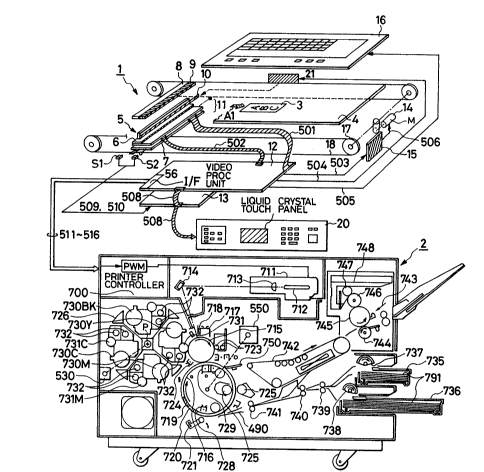
Fig. 1 schematically shows the construction of a
digital color image processing system which incorporates an
image reading apparatus of the present invention. As will
be seen from this figure, the image processing system has an
upper portion constituting a digital color image reading
15 apparatus 1 treferred to as "color reader", hereinafter) and
a lower portion constituting a digital color image printing
apparatus 2 (referred to as "color printer" hereinafter).
The color reader 1 is capable of reading color image
information of an original image on the basis of different
20 colors, by a combination of a later-mentioned color
separation means and a photoelectric conversion element such
as CCD. The color reader 1 then converts the color
information in different colors into electrical digital
image signals corresponding to the respective colors. ~he
25 color printer 2 is a laser beam color printe~ of
electrophotographic type which is capable of reproducing
1~ 1 31 ~20,
1 color images of different colors in accordance with the
digital image signals and performing a plurality of transfer
cycles so as to print a color image in the form of digital
dot patterns on a recording paper.
A description will be made first as to the color reader
1. The color reader has an original 3, a platen glass 4
for carrying an original, a halogen exposure lamp 10 by
which the original is scanned, a rod array lens 5 which
receives and collects light reflected by the ori~inal, and a
10 real-size full-color sensor 6 into which a light image is
input by the rod array lens. The rod array lens 5, the
real-size full-color sensor 6, and the halogen exposure lamp
10 in combination constitute an original scanning unit 11
which is movable in the direction of an arrow Al whereby the
15 original is scanned. The color-separated image signals
obtained through scanning over each scan line are input to a
sen30r output signal amplifier circuit 7 so as to be
amplified to a predetermined voltage level. The amplified
signals are input through a signal line 501 to a video
20 processing unit 12 and are processed by this unit in a
manner which will be detailed later. In order to ensure a
high fidelity of signal transmission, the signal line 501 is
constituted by a coaxial cable. Another signal line 502 is
intended for transmitting driving pulses for driving the
real-size full-color sensor 6. All the pulses necessary for
1~ 1 31 6207
1 driving the full-color sensor 6 are produced in the video
processing unit 12. Numerals 8 and 9 denote, respectively,
white and black boards for use in white-level correction and
black-level correction which will be explained later. More
specifically, the white and black boards 8 and 9 are adapted
to be illuminated by the halogen exposure lamp 10 and are
suitably processed thereby forming signals of predetermined
levels which are used in white-level correction and black-
level correction of the video signal. A reference numeral
10 13 designates a control unit having a microcomputer. The
control unit 13 performs various controls: namely, control
of display and key-input on the control panel 20 through a
BUS 508; control of operation of the video processing unit
12; control of the stepping motor driving circuit for
15 driving a stepping motor 14 which drives the scanning unit
11 through the signal line 502 in response to position
signals representing the position of the scanning unit 11
detected by position sensors Sl, S2 and transmitted through
signal lines 509, 510; control of the state of the halogen
20 exposure lamp 10, as well as the quantity of light from the
sam~e, by means of an exposure lamp driver which in turn is
controlled through the signal line 504; and all types of
control necessary in the color reader unit l including the
control of a digitizer 16, control of internal keys and
25 control of display unitæ. The color image signals read by
1~ 1316207
1 the exposure scanning unit ll during the scanning operation
are input to the video processing unit 12 through the
amplifier circuit 7 and the signal line 501, and undergo
various processings conducted in this unit 12 as will be
S explained later. The thus processed color image signals
are sent to the printer unit 2 through an interface circuit
56.
A description will be made hereinunder as to the color
printer 2. The color printer 2 has a scanner 711 which
10 includes various parts such as a laser output unit for
converting the image signals from the color reader 1 into
light signals, a polygon mirror 712, e.g., an octagonal
mirror, a motor (not shown) for rotationally driving this
polygonal mirror, and an f/~ lens ~image-forming lens) 713.
15 A reference numeral 715 designates a photosensitive drum.
The laser beam emitted from the laser output unit is
reflected by the polygon mirror 71Z onto the surface of the
photosensitive drum 715 thereby to raster-scan the surface
of the photosensitive drum 715, whereby a latent image
20 corresponding to the original image is formed on the surface
of the photosens;tive drum 715.
The color printer 2 further has a primary charger 717,
a whole exposure lamp 718, a cleaner unit 723 for collecting
residual toner particles which have not been used in the
25 image transfer, and a pre-transfer charger 724. The
18 1 31 6207
1 primary charger 717, whole exposure lamp 718, cleaner unit
723, and the pre-transfer charger 724 are arranged around
the photosensitive drum 715.
A reference numeral 726 designates a developing unit
s capable of developing the electrostatic latent image formed
on the surface of the photosensitive drum 715. The
developing unit 726 includes developing sleeves 731Y, 731M,
731C and 731Bk which are adapted for conducting development
upon direct contact with the photosensitive drum 715 toner
10 hoppers 730Y, 730M, 730C and 730Bk for preserving toner
particles and a screw 732 for conveying the toner as the
developer. These parts of the developing unit 726 are
arranged around the axis P of rotation of the developing
unit. When an yellow toner image is to be formed, the
15 development is conducted in the illustrated position by
means of the yellow toner, whereas, when a magenta toner
image is to be formed, the developer unit 726 is rotated
about the axis P in the drawings so as to bring the
developing sleeve 741M into contact with the photosensitive
20 drum 715. Development in other colors, i.e., cyan and
black, can be conducted in the same manner.
The toner image formed on the photosensitive drum 715
is transferred to a paper by means of a transfer drum 716.
A reference numeral 719 designates an actuator plate for
25 detecting the position of the transfer drum 716. More
19 1316207
1 specifically, a position sensor 720 is adapted to produce a
signal representing that the transfer drum 716 has been
brought to the home position, as it is brought to a-position
near the actuator plate 719. The color printer 2 further
s has a transfer drum cleaner 725, a paper retaining roller
727, a charqe eliminator 728 and a transfer charger 729.
These parts 719, 720, 725, 727 and 729 are arranged around
the transfer roller 716.
The copy paper sbeets are fed selectively from paper
10 cassettes 735, 736 by means of paper feed rollers 737, 73~.
The feed and convey of the printing paper sheet are
controlled by means of timing rollers 739, 740 and 741. The
paper sheet which has been fed by the feed rollers is guided
by a paper guide 749 and is wound on the transfer drum 716
lS with its leading end gripped by a later-mentioned gripper so
as to be sent to an image-forming process.
A reference numeral 550 designates a drum motor which
drives the photosensitive drum 715 and the transfer drum 716
in such a manner that these drums rotate in synchronism with
20 each other. A reference numeral 750 designates a separator
claw for separating the copy paper sheet from the transfer
drum 716 after completion of formation of the image. A
numeral 742 denotes conveyor belts for conveying the copy
paper sheet after separation from the transfer drum 716. A
25 num~ral 743 designates an image fixing unit for fixing the
1 31 6207
1 image on the copy paper sheet which has been conveyed by the
conveyor belts 742. The image fixing unit 743 has a pair
of heat-pressing rollers 744 and 745.
A description will be made hereinunder as to the
control unit 13 of the reader unit, with specific reference
to Fig. 2.
(Control Unit)
The control unit includes a CPU 22 which is a
microcomputer. The control unit is adapted for performing
10 various types of control such as the control of the video
processing, control of the lamp driver 21 for effecting
exposure and scanning, control of the motor driver 15,
control of the digitizer 16 and the control of the control
panel 20. These controls are performed through signal
15 lines (BUSes) 508, 504, 503 and 505 and in accordance with
programs stored in the ROM 23 and RAMs 24 and 25, so as to
obtain desired copy of the image. The RAM 25 is backed-up
by a series of batteries 31 which ensures non-volatile
nature of this memory. The signal line 505 is constituted
20 by a line which is ordinarily used for the purpose of serial
signal transmission. The signals transmitted through this
signal line are input by the operator through the digitizer
16, in accordance with the protocol between the CPU 22 and
the digitizer 16. More specifically, signals input through
25 the signal line 505 are, for example, instruction signals
2~ 1 3t 6207
1 for appointing coordinates or regions in editorial
operations such as shiting and synthesis of images,
instructions for selecting a copy mode, instructions for
determining the magnification, and so forth. The signal
line 503 is adapted to transmit signals from the CPU 22 to
the motor driver 15 for givirg instructions concerning the
scanning speed, scanning distance and scanning direction.
Upon receipt of the instructions from the CPU 22, the motor
driver 15 delivers predetermined pulses to the stepping
10 motor 14 thereby operating the motor so as to attain the
desired movement of the scanning unit. The serial I/Fs 29,
30 may be ordinary ones which may be realized by, for
example, by serial I/F LSIs such as Model 8251 available
from IN~EL Co., ~td. Although not shown in the drawings,
I5 similar circuits are also provided in the digitizer 16 and
the motor driver 15. Fig. 3 shows the protocol of the
interface between the CPU 22 and the motor driver 15.
Sensors Sl and S2 are provided for detecting the
position of the original exposure scanning unit 11 (see Fig.
1). More specifically, the sensor Sl detects that the
original exposure scanning unit is in the home position
where the white-level correction of the image signal is
conducted. On the other hand, the sensor S2 detects that
the original exposure scanning unit is on the leading end of
~5
2~ 1 3 1 6207
1 thle image. This position is used as the original reference
position.
(Printer Interface)
Referring to Fig. 2, signals ITOP, BD, VCLK, VIDEO,
~SYNC and SRCOM (511 to 516) are signals for the interface
between the color printer unit 2 and the reader unit 1.
The image signal VIDEO 514 as read by the reader unit 1 is
transmitted to the color printer unit 2 in accordance with
the above-mentioned signals. More specifically, the signal
10 ITOP is a synchronizing signal for attaining synchronism in
the direction of feed of the image. This direction will be
referred to as "sub-scan direction", hereinafter. The
si~nal ITOP is produced once for each color in the
transmission of signals corresponding to one frame of image.
15 Thus, in case of transmission of four-color image
constituted by yellow, magenta, cyan and black, four pieces
o signals I~OP are produced in the transmission of one
frame. This signal is timed to be in synchronism with the
rotations of the transfer drum 716 and the rotation of the
20 photosensitive drum 715 so that the leading end of the copy
paper sheet wound on the transfer drum 715 may be aligned
with the image on the leading end of the original when the
toner image on the photosensitive drum 715 is transferred to
the copy paper sheet at the nip between both drums 715 and
25 716. To this end, the signal ITOP is input as an
23 1 31 6207
1 interruption 511 to the CPU 22 in the controller 13. The
CPV 22 performs control of the image in the sub-scan
direction for the purpose of. for example, edition, in
accordance with the ITOP interruption. A synchronizing
signal BD 512 is produced once per each rotation of the
polygonal mirror 712, i.e., per each raster scan so as to
attain synchronism of signals in the direction of the raster
scar,. This direction will be referred to as "main-scan
direction", hereinafter. The reader unit 1 produces image
10 signals upon reading the original, and the thus obtained
image signals are delivered to the printer unit 2 in a line-
by-line fashion in synchronism with the synchronizing
signals BD. A symbol VCLK 513 is a synchronizing clock
signal for delivering an 8-bit digital video signal to the
15 color printer unit 2. For instance, the 8-bit digital video
signal is transmitted through flip-flops 32 and 35, as shown
in Fig. 4B. A horizontal synchronizing signal HSYNC 515 is
a signal for attaining synchronization of signals in the
direction of the main scan and i8 produced in
20 synchronization with the VCLK 513 in accordance with the
signal BD. The signal HSYNC has the same period as the
signal BD. More strictly, the video signal VIDEO is
produced in synchronization with the horizontal
synchronizing signal XSYNC 515, for the following reason.
25 The signal BD is generated in synchronization with the
24 1 31 6207
1 rotation of the polygon mirror 712, so that this signal
inevitably contains jitter components produced by the motor
for driving the polygon mirror 712. Therefore, if the
signal VIDEO 514 is produced in synchronization with the
signal BD, the signal VIDEO 514 inevitably contains jitter
components. To overcome this problem, the signal VIDEO 514
is generated in synchronization with the horizontal
synchronizing signal ~SYNC 515 which in turn is generated in
accordance with the signal BD in synchronization with the
10 synchronizing clock VCLK which does not contain any jitter
component. The signal line SRCOM is a semi-double signal
line for by-directional serial signal transmission. As
shown in Fig. 4C, a command CM is delivered in
synchronization with an 8-bit serial clock SCLK which is
15 delivered in a period between successive synchronizing
signals csusY (command busy) which are delivered from the
reader unit. In response to this command CM, the printer
unit transmits a status signal ST in synchronization with an
8-bit serial clock produced in a period between successive
20 SBUSY (status busy) signals. The timing chart in Fig. 4C
shows that a status signal "3C~" is sent back in response to
a command "8EH". Thus, instructions from the reader unit
to the printer unit, e.g., appointment of color mode and
selection of cassette, as well as information concerning the
25 statug of the printer, e.g., jamming of paper, absence of
t 31 6207
1 paper, wait.and so forth, are transmitted through this
signal line SRCOM.
Fig. 4A is a timing chart illustrating the timing of
transmission of signals constituting a four-color image, in
accordance with the signals ITOP and HSYNC. A signal ITOP
Sll is produced once per each rotation or every other
rotations of the transfer drum 716. More specifically, an
yellow image, a magenta image, a cyan image and a black
image are delivered from the reader unit 1 to the printer
10 unit 2 in the periods ~ , ~ , .~ and ~ , respectively,
whereby the four color images are superposed so as to form a
full color image on the transfer paper. Assuming here that
the original image of A-3 (420 mm long) is to be read at a
density of 16 pee/mm in the direction of feed, the
15 horizontal synchronizing signal HSYNC is produced 6720 times
(420 x 16 = 6720). The signal HSYNC also is delivered to
the clock input of a timer circuit 28 in the controller
circuit 13. When a predetermined number of signals HSYNC
has been counted, an interruption ~INT S17 is delivered to
20 the CPU 22. The CPU 22 conducts various controls of image
such as extraction or shift of image in the direction of
feed, in response to the interruption HINT 517.
(Video Processing Unit)
A detailed description will be made hereinunder as to
2~ the video processing unit 12, with specific reference to
I 3 1 6207
2 b
1 Fig. 5. As the first step, the original is illuminated by
the exposure lamp 10 (see Figs. 1 and 2) and the light
reflected from the original is read in a color-separated
manner by the color reading sensor 6 in the scanning unit
11. The output from the color reading sensor 6 is
amplified by the amplifier circuit 42 to a predetermined
}evel. A reference numeral 41 designates a CCD driver
adapted to supply a pulse signal for driving the color
reading sensor 6. ~he original pulses for forming this
10 pulse signal are generated by a system control pulse
generator 57.
Figs. 6A and 6B show, respectively, the color reading
sensor and the driving pulses, respectively. Referring
first to Fig. 6, the color reading sensor used in this
lS embodiment has five sensor elements or chips 58 to 62
arranged in a staggered manner such that each sensor chip
reads corresponding one of five sections which are formed by
sectioning the original image in the direction of the main
scan. Each sensor chip has 976 pixels, each pixel having a
20 length of 62.5 ~m (1/16 mm). Since each pixel is divided
into three regions corresponding to G, B and R, the total
number of effective pixels is given by 1024 x 3 = 3072.
The sensor chips 58 to 82 are formed on a common substrate
in such a staggered manner that the first, third and fifth
25 sensor chips 58, 60 and 62 are positioned on a line LA,
2/ 1 31 6207
1 while the second and fourth sensor elements 59, 61 are
disposed on a line LB which is offset from the line LA by an
amount corresponding to four scanning lines (62.5 ~m x 4 =
250 ~m) in the direction of the sub-scan which is conducted
in the direction of an arrow AL in Fig. 6A. In operation,
the first, third and fifth sensor chips 58, 60 and 62 are
driven by a group of driving pulses ODRV 518 in
synchronization with one another, while the second and
fourth sensor elements 59, 61 are driven by another group of
10 driving pulses EDRV 519. As will be seen from Fig. 6B, the
driving pulse group ODRV 518 includes pulses OolA, 002A and
ORS which are charge transfer clocks and charge reset pulse
for each sensor chip of this group. Similarly, the driving
pulse group EDRV 518 includes pulses EOlA, E02A and ERS
15 which are charge transfer clocks and charge reset pulse for
each sensor chip of this group. In order to eliminate any
mutual interference and noise between the first group of
sensor chips including first, third and fifth sensor chips
and the second group including the second and fourth sensor
20 chips, the above-mentioned clock and reset pulses are
produced in a ~ubstantially perfect synchronism so as to
exclude any jitter.
These pulses therefore can be produced by a common
o~cillation source OSC 58' ~see Fig. 5). Fig. 7A is a
25 block diagram of the circuit for generating the driving
2~ 13~6207
1 pulse groups ODRV 518 and EDRV 519, while Fig. 7B is a
timing chart illustrating the operation of this circuit.
This circuit is included by the system control pulse
generator 57 shown in Fig. 5. The single occillation
5 `source OSC 58' produces original clocks CLKO which are
demultiplied to provide clocks KO 535 which are used as
clocks for generating reference signals SYNC2 and SYNC3
which in turn are used in the determination of timings of
generation of the driving pulse groups ODRV and EDRV. The
10 timings of generation reference slgnals SYNC2 and SYNC3 are
determined by values which are set in pre-settable counters
64 and 65 through a signal line 539 connected to the CPU
BUS. These reference signals SYNC2 and SYNC3 are used for
initializing demultipliers 66, 67 and the driving pulse
15 generating portions 68, 69. Thus, the pulses of groups
ODRV 518 and EDRV 519 are generated in synchronization
without any jitter, because they are produced in accordance
with syn~hronous clocks formed by demultiplying the original
clock CLKO produced by a single oscillation source OSC in
20 accordance with the horizontal synchronizing si~nal HSYNC
input to this block, whereby any disturbance of signals
attributable to interference between the sensor chips is
eliminated. The sensor driving pulses ODVR 518 and EDRV
519 are respectively supplied to the odd-number sensor
25 chips, i.e., the first, third and fifth sensor chips, and to
2 9 1 31 6207
the even-number sensor chips, i.e., the second and fourth
sensor chips. In response to these driving pulses, the
sensor chips 58, 59, 60, 61 and 62 independently produce
video signals Vl to V5 in synchronization with the driving
pulses. These video signals Vl to V5 are amplified to
predetermined voltage levels by amplifier circuits 42 which
are provided independently for the respective channels, and
are input to the video processing unit through a coaxial
cable 501 (see Fig. 1). More specifically, the video
signals Vl, V3 and V5 are input at a timing of OOS S29,
while the video signals V~ and V4 are input at a timing of
EOS 534.
Thus, color image signals corresponding to the five
sections of the original in the direction of main scan are
read and input tpo the video processing unit 12. The thus
formed color image signals are color-separated into three
color components of G ~green), B (blue) and R (red) by means
of the sample hold circuit S/H 43. Thus, 15 ~3 x 5 = 15)
signal processing systems are required for processing the
image signals after the sample hold S/H. The construction
and operation of the sample hold circuit S/H 43 will be
explained later in more detail. As will be explained also
with reference to Fig. 8B, the color image signals of the
respective channels after the sample-hold processings are
input to the A/D conver~ion circuit subsequently to
. .
1 31 6207
1 amplification. The video signals input to the A/D
conversion circuit are multiplexed to become digital data
A/Dout. The timing of generation of the digital data Dout
is shown in Fig. 8C, while Figs. 8A and 8B show processing
blocks.
The analog color video signals produced by the 5-chip
real-size color sensor are input to the analog color signal
processing circuits which are provided, as shown in Fig. 8A,
for the respective channels. Since the circuits A to E of
10 the respective channels have the same construction, the
construction and operation of the circuit A will be
explained by way of examplel with reference to Fig. 8A
showing the processing block diagram and Fig. 8C showing the
timing chart.
Referring first to Fig. 8C, the analog color video
signal SiG A includes G, B and R components which appear in
the mentioned sequence. ~s will be seen from Fig. 8D, the
analog color video signal is a composite signal which
includes, in advance of the 3072 effective pixels, a vacant
transport portion which is not connected to the photodiode
of the color sensor and constituted by 12 pixels, a dark
output portion ~optical black) corresponding to 24 pixels
shielded by Ae on the photodiode, and, after the effective
piX21S, 24 dummy pixels. Thus, the analog color video
2S signal SiG A includes 3156 pixels in total.
3l 1 31 ~207
1 The composite analog color video signal SiG A is input
to the amplifier 250 and is amplified to a predetermined
signal output level. At the same time, the component of
this composite signal, which causes the DC level of this
signal to oscillate in an AC-like manner, is removed. Then,
a zero-level clamp is effected by the feedback clamp circuit
251 in order to fix the DC level of the signal SiG A at a
level optimum for the operation of the amplifier 250. The
feedback clamp circuit 251 is constituted by a sample hold
10 circuit S/H 251b and a comparator amplifier 251a. In
operation, the output level of the dark output portion
(optical black) of the analog color video signal SiG A from
the amplifier 250 is detected by the sample hold circuit S/H
215b and is compared by the comparator amplifier 251a with a
15 reference voltage Ref 1 ~Ref 1 = GND in the described
embodiment) which is received by the minus input of the
comparator amplifier 251a. The difference determined
through the comparison is fedback to the amplifier 250 so
that the level of the dark output portion of the output from
20 the amplifier 250 is always fixed at the level of the
reference voltage Ref 1. A signal DK represents the length
of the dark output portion of the analog color video signal
SiG A. This signal is delivered to the sample hold circuit
S/H 251b so that the DC level of the dark output portion of
32 t 31 62 07
the signal SiG A is detected once per each period of
horizontal scanning.
The output of the amplifier 250 is color-separated into
G, ~ and R by the sample hold circuit S/H 43 and is
amplified so as to suit to the dynamic range of the A/D
conversion circuit. Since the same process is conducted for
all color video signals, the process conducted on the B
signal will be explained by way of example. Thus, the same
process is conducted for the G and R signals. ~he
composite output signal from the amplifier 250 is delivered
through a buffer circuit 252 to the sample hold circuit S/H
253 which operates to sample only the pixel outputs
corresponding to the B signals of the composite signal.
The thus color-separated B signal 538 is input to a low-pass
filter(LPG) 256 after amplification through amplifiers
Z54, 255. The low-pass filter 256 removes a component of
frequency of the sampling pulse from the S/H output signal
derived from the S/H circuit 253, whereby only the variance
of the sampled S/H output signal is extracted.
Representing the driving frequency of the CCD by fD,
therefore, each color signal sampled by the sample hold
circuit S/H 253 is a discrete signal having a frequency of
fD/3. It is thus possible to obtain the above-described
effect by using, as the filter 256, a nyquist filter having
a cut-off frequency of fc = (fD/3) x 1/2 - fD/6. It is
3~i 1316207
1 thus possible to extract only the variance of the signal and
to reduce the frequency band width of the subsequent signal
processing systems.
As described, the low-pass filter 256 outputs a color
signal of each color which contains only the signal
component. This color signal is then processed through an
amplifier 257, a white-correction multiplier 258 and a
buffer amplifier 259 under the control of the CPU, whereby
the gain of the signal is controlled as shown by G in Fig.
10 8E. The color signal of each color after the gain control
is then clamped at any desired DC level by a feedback clamp
system which is constituted by a black-level correction
multiplier 260 and a feedback clamp circuit 261. The
operation of this feedback clamp system is identical to that
15 Of the feedback clamp circuit 251. As will be seen from
Fig. 52A, in this embodiment, the multiplier 258 is a
multiplying DAC (D/A converter) which is constituted by a
multiplying DAC 251, operation amplifier 522 and a latch
523, and is adapted to produce an output Vout which is qiven
20 as Vout = -V IN/N (0 < N < 1), where, N represents a binary
fractional value of the input digital code. The function
of a basic multiplying DAC circuit is similar to that of an
analog potentiometer which is unloaded by an operation
amplifier. In other words, this circuit is a voltage
follower constituted by a feedback circuit and a trim
34 1 31 6207
1 circuit (variable resistor circuit) connected to the
feedback circuit, the resistance value of the trim circuit
being variable in accordance with data from the data BUS
508. Therefore, in a channel connecting correction which
will be explained later, the image data produced by the
scanning unit upon reading a white board is amplified to a
level which is determined by the digital data set in an
internal latch 523 through the data BUS of the CPU 22.
Fig. 52B shows the relationship between this digital data
10 and the gain of the multiplier 258. The latch 523
constitutes the I/O of the CPU 22. Setting of data in this
latch is performed through the control lines WR and SEL.
A description will be made hereinunder as to the
feedback clamp system constituted by the feedback clamp
15 circuit 261. This feedback clamp system has a construction
which is substantially the same as the feedback clamp
circuit of the preceding stage. More specifically, the sole
point of difference resides in that, in the feedback clamp
system, the multiplier 260 controlled by the CPU is
20 connected as the reference voltage Ref 2 of the feedback
clamp circuit constituted by the sample hold circuit 261b
and the comparator amplifier 261a. This arrangement is
adopted for the purpose of enabling the color signals
amplified through the amplifier 257, multiplier 258 and the
25 buffer amplifier 259 to be clamped at the level of the
3~ 1 31 6207
1 reference voltage Ref 2 which is varied by the multiplier
260 in accordance with the level determined by the digital
data set in the internal latch 537 through the data BUS 508
of the CPU 22, for the purpose of shifting the level of a
black level signal which is produced by reading a black
board in the channel connecting correction which will be
explained later. This corresponds to the process O shown
in Fig. 8A. The latch 537 is allocated as an I/O of the CPU
22,and setting of data therein is conducted through control
10 lines WR and SEL.
As will be seen from Fig. 53A, the multiplier 260 is a
four-quadrant mode multiplier composed of a multiplying DAC
531, operation amplifiers 532, 533, resistors 534, 535
having a resistance value R and a resistor 536 having a
15 resistance value 2R. The multiplier 260 produces, as shown
in Fig. 53B, a bi-polar voltage output in accordance with
the 6-bit digital data which is set in the internal latch
537 by the CPU.
Thus, the color signals 541(G), 542(B) and 543(R) are
20 gain-controlled and then clamped such that their black
levels are set at a predetermined level. These color
signals are then multiplexed into a single system signal by
an MPX 260 in accordance with multiplex pulses GSEL, BSEL
and RSEL (544 to 546), and the thus-formed single system
25 signal is input into an A/D converter 45 80 as to be
3~ 13162~7
1 converted into a digital signal in accordance with A/D clock
547, whereby digital data AGOUT 548 is obtained as the
output. Representing the reference voltage of the A/D
converter 45 by Vref, since the resolution of the A/D
conversion is 8 bits, the A/D conversion is conducted under
the condition of 1 LSB = Vref/28. According to this
arrangement, the A/D conversion is conducted after the
multiplexing operation performed by the MPX 260. Thus, five
A/D converters each having three systems for three colors
10 are used, and, hence, 15 signal processing system in total
are employed. The described arrangement is adopted also for
other circuits B to E in ~ig. 8A.
<Construction and Operation of FiFo Memory>
As will be understood from the foregoing description,
lS in this embodiment of the present invention, the image of
the original is read by a sensor which has five sensor chips
which correspond to five sections of the original in the
direction of the main scan and which are arranged in a
staggered manner with an offset corresponding to four lines
20 Of main scan (62.5 ~m x 4 = 250 ~m) in the~direction of the
sub-scan. In consequence, the leading channels constituted
by the sensor chips 2,4 and the trailing channels 1,3,5 read
different portions of the original image which are offset
from each other in the direction of the main scan. In order
to properly connect the data read by these two groups of
3~ 1316207
channels, this embodiment of the invention employs a memory
device capable of storing data corresponding to a plurality
of lines. The construction of this memory device is shown
in Fig. 9B. Namely, the memory device has a FiFo-type
arrangement constituted by memories 70 to 74 each storing
data corresponding to a plurality of lines. More
specifically, the memories 70, 72 and 74 are capable of
storing data corresponding to five lines each of which
includes 1024 pixels, while memories 71 and 73are capable of
storing data corresponding to l5 lines. Writing of data is
conducted in a line-by-line fashion from a point indicated
by a last pointer WPO 75 and WPE 76. After writing of one-
line data, the content of the line pointer WPO or WPE is
incremented by +1. The line pointer WPO 75 i8 used
commonly for the odd-number channels 1,3,5, while WPE 76 is
used com~only for the even-number channels 2,4.
The values of the line pointers WPO 75 and WPE 76 are
initialized to the starting values by signals OWRSl' 540 and
EWRST 541. ORST 542 and ERST 543 are signals for
initializing the read pointer to starting value. A
description will be made as to the channels 1 and 2 by way
of example. As will be seen from Fig. 9A, the channel 2 is
ahead of the channel 1 by an amount corresponding to four
lines. Therefore, the timing of reading of a line, e.g.,
line ~ , by the channel 1 is delayed by a period
.
~ 3t 6207
1 corresponding to four scanning lines after the timing of
reading of the same line ~ by the channel 2. It will be
understood that, by putting the writing pointer WPE ahead of
the writing pointer WP0 by an amount corresponding to four
scanning lines and then reading the content of the FiFo
memory at the same timing, data concerning the same line are
obtained from the channels 1,3,5 and the channels 2,4,
whereby the offset of the sensor chips in the direction of
the sub-scan is compensated. For instance, referring to
10 Fig. 9B, the writing pointer WPO points the first line 1 for
the channel 1, while the writing pointer WPE for the channel
2 points the fifth line 5. As the scanning is conducted
from this state, the pointer WPE points 9 when 5 is pointed
by the pointer WPO, and the data of the line ~ of the
15 original is written on the regions of the memories
corresponding to the pointer value 5 in each memory. Then,
reading operation is conducted cyclically while advancing
the read pointers PRO and PRE in the same manner. Fig. 9C
is a timing chart for conducting the above-described
20 control. The image data is delivered in a line-by-line
fashion in synchronization with the synchroni~ing signal
HSYNC. Signals EWRST 541 and OWRST 540 are generated with
an offset of four lines from each other as illustrated. The
signal ORST S42 is produced at an interval corresponding to
25 the capacity of each FiFo memory 70, 72, 74, i.e., for every
39 t 31 6207
1 five scanning lines. Similarly, the signal ORST 542 is
produced at an interval corresponding to the capacity of
each FiFo memory 71, 73 i.e., for every fifteen scanning
lines. The reading is commenced with the reading of one-
s line data from the channel 1 at a speed which is five timeas high as~the writing speed, followed by reading from the
channel 2,channel 3, channel 4 and channel 5, whereby the
signals read from the successive channels 1 to 5 are
connected in series within the period of one horizontal
10 synchronizing signal HSYNC. Referring to Fig. 9D, IRD to
SRD (544 - 548) are signals which represent valid re~ions of
reading operaiton from the respective channels. The described
control for connecting the video signals from the successive
channels by means of the FiFo memory is conducted by a
15 control signal which is produced in a memory control circuit
57' shown in Fig. 5. The circuit 57' is composed of a
discrete circuit such as a TTL. Detailed description of
this circuit is omitted because this circuit does not
constitute any critical portion of the present invention.
20 The memory mentioned before has three color components:
na~ely, a blue component, a green component and a red
component, although the description has been made with
respect to one color component. It will be understood that
the same arrangement is adopted for other color components
25 of the memory.
4~ 1 31 6207
1 <Constructions and Operations of Black and White Level
Correction Circuits>
Fig. 10A shows a black level correction circuit. When
the quantity of light received by the sensor is small, the
black level outputs from the channels 1 to 5 exhibit large
fluctuation between chips and between pixels, as shown in
Fig. 10B. If these outputs are directly used in the
production of the output image, defects such as scores or
local darkening is formed in the data area of the image.
10 Such scores are generated in the regions of high density so
that they are particularly noticeable due to visual
characteristics of the human eyes, even if these scores are
slight. It i5 therefore necessary to conduct the dark
correction so as to compensate for the influence of the
15 fluctuation in the black output. In the described
embodi~ent, this correction is conducted by the black level
correction circuit which will be explained hereinunder with
reference to Fig. 10A. In advance of the copying
operation,the original scanning unit is moved to the
20 position of a black board (see Fig. 9) which is provided on
the leading end of the original table and which has a
uniform density of black color. Then, the halogen lamp is
turned on so that the black level video signal is input to
the black level correction circuit. More specifically, in
25 order that a black level video signal corresponding to one
41 t 31 6207
1 scanning line is stored in a black level RAM 78, a selector
82 operates to select A ~ , white a gate 80 is closed ~
and a gate 81 is opened. In consequence, the data line 551
is connected to data line 553 through data line 552. On the
other hand, a signal ~ is output so that the output of the
address counter 84, which is initialized by ~SYNC, is
received by the address input of the RAMr whereby the black
level signal corresponding to one scanning line is stored in
the RAM 78. This mode of operation for storing the black
10 level signal will be referred to as "black reference value
pickup mode" hereinafter.
The amplitude of the thus picked-up black level data is
extremely small 80 that it tends to be largely affected by
noises which are introduced through various lines from the
15 exterior or through radiation. ~he use of the thus picked-
up black level data is not preferred because it causes the
black image to be coarsened by the noises. To overcome
this problem, the black level data stored in the RAM 78 as
shown in Fig. 10C is subjected to a computation which is
20 conducted in accordance with a flow chart shown in Fig. 10D,
thereby to eliminate the influence of the noises. In Figs.
10C and 10D, a symbol Bi represents the address in the RAM
78, while (Bi) represents the data contained in the address
Bi of the RAM 78. It is assumed here that the original has
25 a length corresponding to the length of an A-4 size paper in
4~ 1 31 6207
1 tlqe direction of main scan. Thus, provided that the pitch
of the pixel is 16 pee/mm, it is necessary to use 4752
pixels/color (16 x 297 mm = 4752). In order to cover this
length of the original, five CCD chips each being 61 mm long
are arranged to form a linear sensor. Thus, the total
number of pixels used is 4880 pixels/color (16 x 61 x 5 =
4880). This means that the suffix i of the address Bi can
take one of the values from 1 to 4880.
Referring to Fig. lOC, the CPU 22 opens the gate 80 and
closes the gate 81 for the latch 85 ~ , ~ , ~ and
and selects the selectors 82, 83 so that the black level
data in the region between the addresses Bi_~ to Bi~; of the
black level RAM 78 shown in (1) of Fi~. lOC is accessed and
read into the work register (RAM 24) of the CPU 22 as shown
in (3) in Fig. lOC. Then, the black level data (Bi_j) to
(Bi~;) in the region between the addresses Bi_j and Bi+j are
added and the sum is divided by the data number 2j~l so as to
be written in the address Mi of the working RAM 24 as the
value of She central pixel Bi. Similar computaSions are
performed from {(Bl) + .... + (8~1) + .... + (B2j~l)} =
(M~l) to {(B4880-2~) + --- + (B48so-;) + --- + (B48so)} =
(M4880-~)- In consequence, the data carried by the central
pixel B~ is written in the RAM 24 as the mean value of the
. data carried by the adjacent pixels B~_~ to B~;, as shown in
(4) in Fig. lOC. Finally, data corresponding to i = J + 1
. . .
43 t 3 ~ 6207
1 is written for the region from i = 1 to i = j, and data
corresponding to i = 4880 - j is written or the region from
i = 4880-j+l to i = 4880. The pixels of addresses from i =
l to i = j and the pixels of addresses from i = 4880 - j + 1
s to i = 4880 are within the invalid regions which are on both
ends of the sensor. (In the illustrated embodiment, j is
assumed to be j = 48.) Then, data in the region between
the addresses Mj~l and M488o_; in the RAM 24 is written again
in the region between addresses Bj~l and M488o-~ of the black
lO level RAM 78, whereby black level data devoid of any noise
is set.
After completion of the described operation for the
blue component in Step B of Fig. lOD, similar computations
are executed for the G signal representing the green
15 component and for the R signal representing the red
component, in Steps G and R, respectively. Although in the
described embodiment the black level data is determined as a
simple mean value of data carried by the central pixel and
adjacent pixels without giving any weight, this is only
20 illustrative and the black level data may be determined by
introducing a concept of weight by multiplying the data of
the respective pixels with different coefficients.
During reading of the image, the memory RAM 78 operates
in data reading mode, so that the data is read from the RAM
25 78 in a line-by-line and pixel-by-pixel fashions and input
4~ t~l6207
1 to the B input of the subtractor 79 through data lines 553
and 557. Namely, in this mode, the gate 81 is closed ~
while the gate 80 is opened ~ . Therefore, in case of the
blue signal for example, the black level correction circuit
output 556 is determined, when the black level data DK(i) is
given, as Bin(i) - DK(i) = sout (i). Similar controls are
performed for the green signal Gin and red signal Rin, by
means of 77G and 77R. In order to execute the described
operation, the control lines ~ , ~ , ~ and ~ o~ the
10 respective selector gates are controlled by the CPU 22 (see
Fig. 2) by means of the latch 85 which serves as an I/O of
the CPU 22.
A description will be made hereinunder as to the white
level correction (shading correction), with reference to
15 Fig. 11-1. The white level correction is executed in
accordance with white color data which is obtained by moving
the scanning unit to the position of a white board of a
uniform white color and illuminating this white board. The
basic circuit arrangement for this correction is shown in
20 Fig. ll-lA. This circuit arrangement is basically the same
as that of the circuit shown in Fig. 10A, except that the
white level correction employs a multiplier 79' in place of
the subtractor 79 used in the b}ack level correction. Other
portions are materially the same so that detailed
25 description thereof is omitted. The white level correction
4~ 1 31 6207
1 is conducted as follows. When the original scanning unit is
stationed on the position of the uniform white board, i.e.,
when the unit is on the home position before commencing the
copying or reading operation, the exposure lamp is lit on so
that the video data of uniform white level is stored in a
one-line correction RA~ 78'. For instance, when the
original has a length corresponding to the length of an A-4
size paper in the direction of the main scan, 4752 pixels
(16 x 297 mm = 4752) are required provided that the pixel
10 pitch is 16 pee/mm. This requirement is met by the use of
five CCD sensor chips each having 976 pixels, because these
five CCD sensor chips provide 976 x S = 4880 pixels in
total. Thus, the RAM has at least 4880 bytes. Referring
to Fig. ll-lB, representinq the white board data of the i-th
15 pixel by Wi (i = 1 to 4880), the RAM 78' stores data
corresponding to the respective pixels as shown in Fig. llC.
When the white board data Wi is given, the data Do obtained
after the correction should satisfy the condition of Do = Di
x FFH/Wi, with respect to the data of ordinary image read
20 from the same i-th pixel. Therefore, the CPU 22 (see Fig.
2) operates to open the gate 81' while closing the gate 80
for the latch 85' ~ ', ~ ', ~ ' and ~ ' and enables the
selectors 82', 83' to select B, thereby enabling the CPU to
make access to the RAM 78'. Subsequently, computations are
25 executed Such as FFH/Wl for the initial pixel Wl, FF/W2 for
4~i 1 31 6207
1 W2 and so foreth, thereby effecting substitution of data.
When this operation is completed with respect to the blue
component in Step B of Fig. ll-lD, similar computations are
conducted for green and red components in Steps G and R,
successively. Then, the gate 80' is opened ~ ', while the
gate 81' is closed ~ ' and the selector 83' selects A, so
that Do = Di x FFH/Wi is output for the original data Di
which are input successively. The thus read coefficient
data FF~/Wi are transmitted through signal lines 553 and 557
10 and is multiplied with the original image data 551, whereby
the product of the coefficient data and the original image
data is output.
A description will be made hereinunder as to the
channel connecting correction which is conducted for the
15 purpose of ensuring that all the chips 58 to 62 of the color
CCD 6 produce signals of the same level when they read the
original images of the same density level, with reference to
flow charts shown in Figs. 11-2A and 11-2B. The black level
processing of B signal for the channel connecting correction
20 is executed in Step D-B. This operation is commenced with
the processing of the black level of the B signal of the
first channel CHl. To this end, in Step D-Bl, the CPV 22
operates to set Dl (80~ inthe illustrated embodiment) in the
latch 537 (see Fig. 53A) in the multiplier circuit 260 (see
25 Fig. 8B), through the data BUS 508, thereby setting the B
4 1 3 t 6207
1 signal offset of the first channel CHl at the reference
level, thus setting data for the multiplying D/A 531 (Step
1). In this state, a black level signal obtained throu~h
reading of the black board is stored in the black level RAM
78 as in the case of the black level correction explained
before (Step 2). The black level data stored in the RAM 78
is shown in Fig. 11-2C. Subsequently, the value i o the
content of the counter is initialized to 1, and FFH is set
in the minimum value storage temporary memory address Ml of
10 the CPU working RAM 24 (Step 3). Subsequently, the data
(Bi) in the black level RAM 78 is compared with the data
(Ml) in the memory Ml. If the value of ~he data (Bi) is
smaller than the value of the data ~Ml), the data (Ml) of
the address Ml is changed to Bi), and this operation is
15 repeated from Bi = Bl to Bi = Bg76, in Steps 4, 5 and 6.
Consequently, the minimum value throughout the channel CHl
is stored in the memory Ml. Then, a judgment is conducted
in Step 7 as to whether the minimum value data in the memosy
Ml is equal to the reference value D2 (08H in the
2Q illustrated embodiment) of the black level. If they are not
equal, the process proceeds to Step 8 in which they are
compared with each other to determined which one of them is
greater. If the minimum value data Ml is smaller than the
reference value D2, the process proceeds to Step 9 in which
25 the CPU sets a value Dl~a in the latch 537 of the multiplying
4'~ 1 31 6207
1 circuit 260. The process then returns to Step 3 and
proceeds to Step 7 in which the judgment is conducted again
as to whether the condition of (Ml) = D2 is met.
Conversely, if the comparison conducted in Step 8 has proved
that the condition of (Ml) > D2 is met, the CPU 22 sets a
value Dl_a in the latch 537 of the multiplying circuit 260 so
as to lower the offset level (Step 10). The process then
returns to Step 3 and proceeds again to Step 7 in which the
judgment is conducted again as to whether the condition of
(Ml) = Dl is met.
As will be seen from the foregoing description, the CPU
repeatedly conducts the operation while varying the data Dl
by substituting Dl+~ or Dl_~ for the data to be input to the
multiplying D/A 531 until the condition of (Ml) = Dl is met.
15 When this condition is met, the process proceeds from Step 7
to Step D-B2, in which the value of the content of the
counter is initialized to 977 and the processing which is
the same as that executed in Step D-Bl for the channel CHl
is conducted for the data from the channel CH2 inthe RAM 78,
20 thereby setting the minimum value at D2. Similarly, Steps
D-B3, D-B4 and D-BS are executed to set the minimum values
of the data from the channels CH3, CH4 and CH5 at D2. The
described process is executed in Steps D-G and D-R for the G
and R signals, respectively, for each of the channels CH2,
49 1 31 6207
1 CH3, CH4 and CH5, thereby setting the minimum values of all
color data of all channels at D2.
Subsequently, Step W-B is executed for the purpose of
white level processings of the B signal in the channel
5 connecting white level processing. First o~ all, Step W-Bl
is conducted for performing the white level processing of
the B signal of the first channel CHl. To this end, the CPU
22 operates so as to set a level D3 (AOH in the illustrated
embodiment) in the latch 523 of the multiplying circuit 258,
10 through the data S 508, thereby setting the gain of the B
signal at a reference level, and so as to set the data of
the multiplying D/A 521 (Step 11). In this state, the
white level signal of the white board is set in the white
level RAM 78' (Step 12) as in the case of the white level
15 correction explained before (Step 11). The white level
data stored in the RAM 78' is shown in Fig. 11-2C.
Subsequently, the value i of the content of the counter is
initialized to 1, and OOH is set in the maximum value
storage temporary memory address M2 of the CPU working RAM
20 24 ~Step 3). Subsequently, the data (Wi) in the white
level RAM 78' is compared with the data (M2) in the memory
M2 . If the value of the data (Wi) is greater than the
value of the data (M2), the data (M2) of the address M2 is
changed to (W~), and this operation i5 repeated from Bi = B
25 to B~ = Bs76, in Steps 14, 15 and 16. Consequently, the
~{~ 1 3 t 6207
1 maximum value throughout the channel CHl is stored in the
memory M2. Then, a judgment is conducted in Step 17 as to
whether the maximum value data in the memory M2 is equal to
a reference value D4 (AOH in the illustrated embodiment) of
S the white level. If the maximum value data (M2) is greater
than the reference value D4, the process proceeds to Step 19
in which the CPU 22 sets a value Dg_~ in the latch 523 of the
multiplying circuit 258 so as to lower the gain level. The
process then returns to Step 13 and proceeds to Step 17 in
10 which the judgment is conducted again as to whether the
condition of (M2) = D4 is met. Conversely, if the
comparison conducted in Step 18 has proved that the
condition of (M2) ~ D4 ~s met, the CPU 22 sets a value D
in the latch S23 of the multiplying circuit 258 so as to
lS raise the gain level (Step 20). The process then returns to
Step 13 and proceeds again to Step 17 in which the judgment
is conducted again as to whether the condition of (M2) = D4
is met.
As will be seen from the foregoing description, the CPU
20 repeatedly conducts the operation while varying the data D4
by substituting D4~ or D4 ~, until the condition of (M2) =
D4 is met. When this condition is met, the process proceeds
from Step 17 to Step W-B2, in which the value of the content
of the counter is initialized to 977 and the processing
25 which is the same as that executed in Step W-Bl for the
51 1 31 62~7
1 channel CHl is conducted for the data from the channel C~2
inthe RAM 78', thereby setting the maximum value at D4.
Similarly, Steps W-B3, W-B4 and W-B5 are executed to set the
maximum values of the data from the channels CH3, CH4 and
s CH5 at D4. The described process is executed in Steps W-G
and W-R for the G and R signals, respectively, for each of
the channels CH2, CH3, CH4 and CH5, thereby setting the
. maximum values of all color data of all channels at D4.
The channel connecting process is executed following
10 the flow chart shown in Fig. 11-3. After the power of the
-reader unit 1 is turned on, the process is started from Step
S-ml in which, if the original scanning unit 11 i9 not set
at the position of the home position sensor Sl, the CPU 22
operates so as to give a home position resetting instruction
15 to the stepping motor driver (see Fig. 2) through the signal
line 503, whereby the stepping motor 14 operates to reset
the original scanning unit 11 to the home position. Then,
in Step S-m2, the CPU produces a lighting instruction to the
lamp driver 21 through the signal line 504, thereby to turn
20 the halogen lamp 10 on. After turning the halogen lamp 10
on, the CPU 22 operates in Step S-m3 so as to set, in the
driver 15, pulses of a number corresponding to the distance
to be traveled by the original scanning unit 11 from the
home position Sl to the position of the reference black
25 board 9, thereby to drive the original scanning unit 11 to
5 2 1316207 `
1 the position of the reference black board. The channel
connecting black level processing explained in connection
with Fig. 11-2A is conducted in this state (Step S-m4).
Subsequently, the process proceeds to Step S-mS in which the
CPU sets in the driver 15 pulses of a number coreesponding
to the distance between the reference black board 9 and the
reference white board 8, thereby driving the original
scanning unit 11 to the position of the reference white
board. The channel connecting white level processing
10 explained in connection with Fig. 11-2B is conducted in this
state ~Step S-m6). Subsequently, the halogen lamp is
turned off in Step S-m7 and the original ~canning unit 11 is
reset again to the home position in Step S-m8.
The channel connecting process is thus completed. It
15 will be understood that the described arrangement and
operation ensure a high speed of processing, while enabling
correction on the basis of each pixel.
It is al90 to be noted that, in the described
embodiment, one-line video data can be inpu~ at a high speed
2Q and can be accessed by the CPU for reading and writing.
This makes it possible to detect the ratio of color
components B, G and R of the video data on a point which is
determined by coordinates (X mm, y mm) on the original, by
driving the original scanning unit 11 in the x-direction by
25 a distance corresponding to (16 x x) lines and then picking
1 31 6207
53
1 up the data of the (16 x y)-th pixel. This mode of
operation will be referred to as "line pickup mode",
hereinafter. It will be obvious to those skilled in the
art that the described arrangement makes it possible to
5 determine a mean density of a plurality of lines (referred
to as "mean value computing mode") and to determine the
density histogram (referred to as "histogram mode").
<Logarithmic Conversion>
Through the processes explained hereinbefore, black
10 level and white level corrections are effected to eliminate
any influence of various factors such as fluctuations in the
black level sensitivity of the video input system, dark
current level, sensor output characteristics, light quantity
in the optical system and white level sensitivity, whereby a
15 color video data proportional to the input light quantity
and uniformalized in the direction of main scan is obtained.
The thus obtained color video data is input to a logarithmic
conversion circuit 86 (see Fig. S) conforming with the
spectral luminous efficiency of human eyes. This circuit 86
20 is adapted to perform a conversion to set the white and
black levels at OOH and FFH, respectively. The conversion
is conducted by making selective use of a plurality of
logarithmic conversion tables LUT ~Look-up Table) as shown
in Figs. 13A and 13B, in accordance with the types of the
25 image source such as ordinary reflective original,
~ 1316207
1 transparent originals such as those used in projectors
including both negative and positive films, and films of
different sensitivities and exposure conditions, because
different types of image source provide different gamma
5 characteristics. The change-over between different LUTs is
conducted through signal lines e90, egl and eg2 (560 to 562),
in accordance with input given from the control unit through
the I/Oport of the CPU 22. The levels of the data given
for the B, G and R colors correspond to the density value of
10 the output image. Thus, the output concerning B (blue)
corresponds to the amount of yellow toner, the output
concerning G (green) corresponds to the amount of magenta
toner, and the output concerning R corresponds to the amount
of cyan toner. In the following description, therefore,
15 the color video data are expressed in terms of Y, M and C.
<Color Correction>
The following color compensation is conducted for the
color component video data, i.e., yellow component, magenta
component and cyan component, obtained from the original
20 image through logarithmic conversion. It is well know that
the spectral characteristics of the color separation ~ilter
provided on the color reading sensor for each pixel has an
unnecessary transmission area as hatched in Fig. 14. It is
also well known that the color toners (Y, M, C) to be
~ 1 31 62~7
1 transferred to the transfer paper have unnecessary
absorption components as shown in Fig. 15.
In order to eliminate unfavorable effects o~ these
unnecessary transmission area and unnecessary absorption
component, various color correction methods have been
proposed and used. For instance, it is well known to
conduct masking correction in which color correction is
performed by computing the following first degree equation
for each color component video data Yi, Mi and Ci.
Yo~ aYl -bMl -CCI ~ ~Yi
Mo = ~ -~Y2 bM2 -CC2 M~
~Co, ~-aY3 -bM3 C~ ~Ci,
In a method known as "inking", the minimum values
15 Min(Y~, M~, C~) of the color component data Yi, Mi, Ci are
computed and black toner is added by treating the minimum
values as black level. An under-color removal (UCR) is also
known in which the amounts of the respective color toners
are reduced corresponding to the amount of the black `
20 component added. Fig. 16A shows the arrangement of
circuits for the masking correction, inking and UCR
operations. This circuit arrangement has the following
featuress
5~ 13162~7
1 (1~ Two masking matrix systems are used, and switching
therebetween can be executed at a high speed by switching of
the level of a signal line between "1" and "0".
(2) Switching between a mode which employs UCR and a mode
5 which does not employ UCR is conducted at a high speed by
switching of the level of a signal line between "1" and "0".
~3) There are two systems of circuit for determining the
amount of inking, and switching therebetween is conducted at
a high speed by switching of the level of a signal line
10 between "1" and "0".
Before the commencement of the reading of the ima~e,
any desired first matrix coefficient Ml and second matrix
coefficient M2 arq set though a BUS connected to the CPU.
In the described embodiment, the following coefficients M
15 and M2 are set in registers 87 to 95 and registers 96 to
104, respectively.
aYI - bMI - Ccl a Y~ - ~ Ml - r Cl~
Ml ~ -ay2 bM2 -CC2 ~ M2=~ - ~ Y2 ~ M2 - 7 C2 )
~ -ay3 -bM3 CC3J ~ - ~ Y3 - ~ M3 ~ C3
Numerals 111 to 122, 135 and 131 denote selectors each
being adapted to select "A" and "B", respectively, when the
level of the S terminal thereof is "1" and "0",
2s respectively. Therefore, the matrix coefficients Ml and M2
5`,. 1 31 6207
1 are selected by setting the switching signal MAREA 564 at
"1" and "0", respectively. Numeral 123 also designates a
selector which provides one of outputs a, band c in
accordance with a truth table shown in Fig. 16B, in response
5 to selection signals Co and Cl (566, 567). The selection
signals Co~ Cl and C2 correspond to the color signals to be
output. Namely, color-corrected Y, M, C and Bk color
signals are obtained by setting the selection signals Co, C
and C2 as (Co~ Cl, C2) = (0,0,0), (0,,0,1), (0,1,0) and
10 (1,0,0), respectively. A color-corrected monochrome signal
is obtained by setting the selection signals Co~ Cl and C~ as
(Co, Cl, C2) = (0,1,1). If the selection signals Co, Cl and
C2 areset as (Co, Cl, Cz) = ~0,0,0) while the MAREA is set as
MAREA = "1", the contents of the registers 87, 88 and 89,
15 i-e., (ayl, -bMl, -ccl) are obtained as the output (a,b,c) of
the selector 123. On the other hand, the black component
signal 574, which is computed as Min(Y~, Mi, Ci) from the
input signals Yi, Mi, Ci, is subjected to a primary
conversion which i8 conducted by 134 in accordance with a
20 formula Y = ax - b (a and bare constants), and is input to
.~
the B inputs of subtractors 124, 125 and 126 through the
selector 135. For the purpose of the under-color removal,
the subtractors 124 to 126 execute computations of Y = Yi ~
(ak - b), M = M~ - (ak - b) and C = C~ - (ak - b),
25 respectively. The results of the computations are input to
5~ 1 31 6207
1 the multipliers 127, 128 and 129 for the masking
computations. The selector 135 is controlled by a signal
~AREA 565 which is capable of conducting a high-speed
switching between a mode which employs the under-color
removal (UCR) and a mode which does not employ the UCR, by
switching of its level between "1" and "0". Each of the
~ultipliers 127, 128 and 129 receives at its A input the
siqnal (ayl, -bMl, -Ccl) and at its B input the signal [ Yi ~
(ak - b), Mi - (ak - b), Ci - (ak - b)l = lYi, Mi, Gil-
10 Therefore, as will be seen from his figure, an output Yout =Y~ x (ayl) + Mi x (-bMl) + Ci x (-Ccl) is obtained at the
output Dout, on condition of C2 = 0 (select Y or M or C),
whereby an yellow video data after masking color correction
and under-color removal is obtained.
Similarly, outputs Mout = Yi x (-ay2) ~ Mi x (bM2) ~ Ci
x (-Cc2) and Cout = Yi x-(-ay3) ~ Mi x (-bM3) + C~ x (Cc3) are
obtained at the output Dout. The color selection is
controlled by the CPU 22 in accordance with the table shown
in Fig. 16B by suitably setting the values (Cn, Cl, C2) in
20 the sequence of development performed by the color printer.
The registers 105 to 107 and 108 to 110 are monochrome image
forming registers and are obtained by weighted addition of
the colors in accordance with the formula of MONO = klY~ +
~IMi ~ mlCi. The switching signals MAREA 564, UAREA 565 and
25 KAREA 587 are for conducting, respectively, the high-speed
1 31 6207
s~
1 switching between the masking color correction coefficient
matrixes Ml and M2, the high speed switching between the
mode which employs UCR and the mode which does not employ
the UCR, and the high-speed primary switching of the black
s component signal which is delivered from the Dout through
the signal line 569 and the selector 131. More
specifically, the KAREA 587 conducts a high-speed switching
between Y = ck - d and Y = ek - f (c, d, e and f are
constant parameters) for a given value K = Min (Yi, Mi, Ci).
10 it is therefore possible to apply different masking
coefficients to different areas of a single image or to vary
the amount of UCR and amount of inking according to areas.
This arrangement,therefore, can be used for synthesizing
images derived Erom different image input sources of
15 different color-separation characteristics or a plurality of
images of different black tone levels, as in the described
embodiment of the invention. The area signals MAREAm UAREA
and KAREA 564, 565, and 587 are produced by an area signal
generating circuit 51 (see Fig. 2) which will be detailed
20 hereinunder.
<Area Signal Generating Circuit>
The principle of generation of the area signals such as
MAREA 564, UAREA 565 and KAREA 587 will be explained with
reference to Figs. 17A to 17G. The term "area" is used to
25 mean, for example, a region which is hatched in Fig. 17E.
~o 1316207
1 This area can be determined by ~eneratin~ a signal AREA at a
timing shown in Fig. 17E in each scanning period in a region
between A and B as measured in the direction of the sub-
scan. Each area can by appointed by the digitizer shown in
5 Fig. 1. Figs. 17A to 17D show an arrangement which enable~
a multiplicity of area signals to be formed in a
programmable manner by the CPU 22. With this arrangement,
therefore, it is possible to provide a variable number o
area signals at variable timings and with variable lengths.
In this arrangement, each area signal is constituted by one
bit of a RAM which is accessible by the CPU 22. For
instance, a pair of RAMs 136, 137 (Fig. 17D) each having n
bits are used for the purpose of generating n-pieces of area
signals AREA0 to AREAn. Thus, area signals AREA0 and AREAn
15 as 8hown in Fig. 17B can be obtained by setting "1" in the
bit 0 at the addresses xl and X3 of the RAMs, while setting
"0" in bits 0 at all other addresses. On the other hand,
"1" is set in the bit n at addresses 1, xl, x2 and x4, while
"0" is set in bit n at all other addresses in the RAM.
20 Then, by sequentially reading the data from the RAM in
synchronization with clocks based on the signal ~SYNC, data
"1~ i8 read at each of the addresses xl and X3 as shown in
Fig. 17C. The thus read data are input to J and K
terminals of the J-K flip-flops 148-0 to 148-n shown in Fig.
25 17D so that a region signal such as AR~A0, i.e., the area
,, ~
~i 1316~07
1 signal, is produced by a toggle operationr i.e., an
operation which changes the output level from "0" to "1" and
vice versa when CLK is input white "1" is read from the RAM.
If data "0" is set in all addresses, the area signal is not
5 generated so that no area is set. Fig. 17D shows the
arrangement of this circuit having the RAMs 136 and 137.
These two RAMs 136 and 137 are used alternately in such a
manner that, while a line data is being read from the RAM
136, data for setting the area is set by the CPU into the
10 other CPU 22 ~see Fig. 2), thereby attaining a high-speed
switching of the area length. For instance, when an area
hatched in Fig. 17F is appointed, the ~AMs A and B are
switched from A to B, from B to A, from A to B and then from
B to A. This operation will be explained in more detail
15 with reference to Fig. 17D. When data (C3, C4, C5) are set
as ~C3, C~, C5) = (O, 1, O), the output from the counter
which counts in synchronization with VCLK is delivered as an
address data to the RAM 136 through a selector 139 ~Aa). At
the same time, a gate 142 is opened white a gate 144 is
20 closed so that the RAM 136 is used in the reading mode to
.,_
allow data to be read therefrom, whereby n-bit data are
input to the J-K flip-flops 148-0 to 148-n, whereby a region
signal ~REA0 to AREAn is generated in accordance with the
value set in the RAM 136. Meanwhile, writing of the data by
the CPU to the RAM B is conducted through an address BUS A-
. ~ .
6~ 1 31 6207
1 Bus and data BUS D-Bus, in accordance with an access signal
R/W. The generation of the region si~nal on the basis o
the data set in the RAM B 137 is conducted in the same
manner, by setting the data ( C3, C4, C5 ) as ( C3, C4, Cs ) =
5 (1, 0, 1). Meanwhile, data is written by the CPU into the
RAM A 136. These two RAMs will be reerred to as A-RAM and
B-RAM, respectively, while the data C3, 4 , Cs will be
collectively referred to as AREA control signai (ARCNT).
The AREA control signal C3, C4, C5 are generated through the
10 I/O port of the CPU. Fig. 17G illustrates a table which
contains correlations between the bits and the names of
signals.
<Color Conver~ion~
The circuit arrangement for color conversion will be
15 explained hereinunder with reference to Fig. 18. The term
ncolor conversion" is used to mean a replacement of an input
color component data (Yi, Mi, Ci) of a specific density or
color component ratio with another color. Practically,
this operation is conducted for changing. for example, the
20 red color of hatched area of the original shown in Fig. 18C
into, for example, blue color. The color data ~Y~, Ml, C~)
input to this circuit is averaged on 8-pixel basis by
smoothing circuits 149, 150 and 151. The average data is
input to an adder 155 which computes (Y~ + Mi + Ci) and
25 inputs the same to the B inputs of dividers 153, 154. The
6;3 1 3t 62a7
1 average data also is input to the A inputs o~ these
dividers, whereby color ratios including the yellow ratio
ray = Yi/(Yi ~ Mi + Ci), magenta ratio ram = Mi/(Yi + Mi ~
Ci) and the cyan ratio rac = Ci/(Yi + Mi + Ci) are derived
through signal lines 604, 605 and 606, respectively, and are
input to the window comparator 156 to 158. These window
comparators 156 to 158 are adapted to produce outputs oE "1"
level on conditions that the values of the color ratios fall
within a ranges between the upper and lower limits (Yu, mu,
10 Cu), (yt, mt~ct)~ Namely, outputs "1" are obtained from the
respective window comparators on conditions of y~ 5 ray <
Yu~ mt 5 ram < mu and ct s rac < cu. The CPU judges that
the input color is the very one which has been expected,
when all of these three conditions are met. When all of
these three conditions are met, a 3-input AND gate 165
produces an output of "1" level. This output is input to
the So input of a selector 175. When the level of the
signal output from the I/O port of the CPU and carried by a
signal line CHGCNT 607 is "1", the adder 155 produces an
20 output 603 =l3Ai. When the same signal is "0", the adder
produces an output 603 = 1. Therefore, when the level o~
the above-mentioned signal is "0", the dividers lS2, 153 and
154 directly deliver the signals received by their A inputs.
Thus, color density data rather than the desired color
25 component ratio are set in the registers 159 to 164. The
6~ 1 3 1 6207
1 selector 175 mentioned above has four input lines and one
output line. The inputs 1, 2 and 3 of the selector 175
receive the Y, M and C components as the color data of the
color to be obtained after the color conversion. Meanwhile,
the input 4 receives the data Vin which has been obtained by
conducting masking color correction and UCR in the read
original image data. Thus, the input 4 is connected to the
output Dout shown in Fig. 16A. The switching input So
ta~es a level "1" when the color detection is "true", i.e.,
10 when a predetermined color is detected, otherwise a level
"O". A symbol Sl is an area signal C~AREA0 615 produced in
the area generating circuit shown in Fig. 17D. This signal
takes "1" level for the data within an appointed area
and "0" for the data which are out of the area. Thus, the
15 color conversion is conducted only when this signal Sl is
set at "1". The inputs S2 and S3 (Co and Cl) 616 and 617
are the same as the signals Co and Cl shown in Fig. 16A.
The color printer performs formation of an yellow image,
magenta image and cyan image conditions of (Co, Cl) = (0,
20 0), (C0, Cl) = (0, 1) and (Co~ Cl) = (1, 0), respectively.
Fig. 18B show~ the truth table for the selector 18B. The
color component ratios to be obtained after the color
conversion or the color density data to be obtained after
the color conversion are set in reqisters 166 to 168 by the
25 CPU. In the area where y', m' and c' are color component
~5 t 3 1 6207
1 ratios, since the CHGCNT 607 has been set to "1", the output
603 of the adder 155 represents (Yi + Mi + Ci) which is input
to the B inputs of the multipliers 169 to 171. In
consequence, the selector inputs 1, 2 and 3 receive,
5 respectively, signals (Yi + Mi + Ci) x y', (Yi ~ Mi + Ci) x
m' and (Yi + Mi + Ci) x c', whereby color conversion is
executed in accordance with the truth table shown in ~ig.
18B. In contrast, when y' t m' and c' are color component
density data, the CHGCNT is set as CHGCNT = "0", so that the
10 signal 603 takes "1" level. Therefore, the inputs 1, 2 and
3 of the selector 175 directly receive the data (y', mm',
c') thereby causing a color conversion through replacement
of the color component density data. As explained before,
the area signal CHAREA0 615 allows the region length and
15 region number to be set freely. It is therefore possible to
apply the color conversion only to a plurality of regions
rl, r2, r~. It is also possible to conduct a high-speed and
real-time color conversion in a plurality of regions with a
plurality of colors, e.g., from red to blue in the region
20 r1, from red to yellow in the region r2 and from white to
~ed in the region r3, by using a plurality of circuit~ shown
in Fig. 18A. Namely, a plurality color detection and
conversion circuits of the same construction as that
explained above are prepared, and a selector 230 selects the
25 desired output from among the outputs A, B,C and D of these
~ 1 31 6207
~b
1 circuits in accordance with signals CHESELO and CHSELl and
the thus selected output is delivered through an output 619.
The area signals CHAREAO to CHAREA3 applied to the
respective circuits, as well as CHSEL0 and C~SELl,are
generated by the area generating circuit 51 as shown in Fig.
17D.
<Gamma Conversion Circuit>
Fig. 19 shows a gamma conversion circuit which is used
for the purpose of controlling the color balance and the
10 color densities of the output image in the described system.
The gamma conversion basically relies upon data conversion
by means of an LUT (Look-Up Table). The data contained in
the LUT can be rewritten in accordance with input from the
control unit. Writing of data in the RAM 177 constituting
15 the LUT iS conducted as follows. By setting the level of
the signal on the selection signal line RAMSL 623 at "0",
the selector 176 selects the B input so that the gate 178 is
closed while the gate 179 is opened, whereby the BUSes ABUS
and DBUS (address data) leading from the CPU 22 are
20 connected to the RAM 177, thus enabling wiring or reading of
data into and from the RAM 177. Once the conversion table
is formed, the RAMSL is set to"l" so that the video input
from the Din 620 is input to the address input of the RAM
177 so that addressing can be done by the video data,
25 whereby the desired data is input through the open gate 178
1 31 6207
6;
1 to the magnification control circuit of the next stage. At
least two types of gamma characteristics (A and ~ in Fig.
1913) are provided in the gamma RAM for five color types of
yellow, magenta, cyan, black and MONO. As in the case of
the operation explained in connection with Fig. 16, the
switching of each color is executed in terms of the data Co,
Cl,C2 (566, 567, 568). In addition, as shown in Fig. l9C,
the area A is provided with a gamma characteristic A, while
the area B is provided with a gamma characteristic B, in
10 accordance with an area signal GAREA 626 generated by the
area generating circuit ~see Fig. 17), whereby both areas of
different gamma characteristics form corresponding images in
a single print.
Thus, the gamma RAM has two types of magnification
15 characteristics A and B which are switchable at a high speed
for independent regions. Obviously, high-speed switching
between three or more magnification characteristics is
obtainable by increasing the type of the magnification
characteristic. The output Dout 625 in Fig. l9A is
20 connected to the input Din 626 of the magnification control
circuit (see Fig. 20A) of the next stage.
As will be seen from the drawings, the described gamma
conversion RAM is constructed to enable the conversion
characteristics to be changed for independent colors. The
25 contents of the RAM can be rewritten by the CPU in relation
1 31 62~7
1 to the operation of liquid-crystal touch panel key on the
control panel.
<Procedure of Gamma Conversion>
Assume here that a density adjusting key e or f on a
S standard picture P000 (see Fig. 33) is touched by the
operator. If the key touched by the operator i5 the key e,
the setting is shifted to the left as from -1 to -2, as will
be seen from Figs. l9D and l9E. The characteristics set in
the RAM 177 also is shifted correspondingly from -1 to -2,
10 from -2 to -3, from -3 to -4 and so on. When the key
touched by the operator is the key f, the characteristics
are shifted as from +l to +2, from ~2 to +3, from ~3 to +4
and so forth, thus rewriting the content of the RAM 177.
Thus, the whole table ~RAM 177) for the Y, M,C, Bk or MONO
15 can be rewritten by touching the key e or the key f on the
standard picture mentioned above, whereby the density of the
image can be changed without causing any change in the color
tone. Fig. 37 shows a picture P 420 displaying a color
balance control function in <color create> mode. The
20 function enables the data for the independent colors Y, M, C
and Bk only within the area of the RAM 177, so as to enable
the color balance to be controlled. For instance, when it
is desired to change the color tone of the yellow component,
the black display belt on the picture P 420 is extended
25 upward in response to pressing of a touch key Yl so that the
~3 1316207
1 conversion characteristic is changed in the Yl direction as
indicated by -Y in Fig. l9F, whereby the density of the
yellow color component is increased. Converselyr when the
touch key Y2 is pressed, the characteristic is shifted in
the direction Y2, whereby the density of the yellow color
component is decreased. Thus, the color balance function
enables the color tone to be changed through a change in the
density of each color component.
<Magnification Control>
Referring to Fig. 20A, numerals 180 and 181 denote FiFo
memories each having a capacity of 16 x 297 = 4752 pixels
(pixel pitch of 16 pee/mm over a length of 297 mm
corresponding to length of A-4 size paper)in the direction
of the main scan. As will be seen from Fig. 20B, each FiFo
15 memory conducts writing of data into the memory throughout a
period of AWE, BWE = "Lo" and reading of data throughout the
period of ARE, BRE = "Lo". The output A and the output B of
the memory is changed into high-impedance state on condition
of ARE = "Hi" and BRE = Hi, respectively. The wired OR of
20 these outputs A and B is then output as the output Dout 627.
Each of the FiFo A 180 and FiFo B 181 is constructed such
that the position of an internal counter is advanced in
accordance with the write address counter and read address
counter (see Fig. 20C) which operate in response to write
and read clocks WCK and RCK. It is therefore possible to
;ù 1 31 6207
1 reduce the size of the output data from this circuit as
compared with the input data, by delivering, as the clock
WCR, a clock CLK which is produced by thinning out the video
data transfer clock CCLK 588 by means of a rate multiplier
630, while directly using the clock VCLK as the clock RCK
without an thinning. Conversely, the size of the output
date is increased as compared with the size of the input
data, if the clock VCLK is directly used as the W~K while
the thinned out clock CLK is used as the clock RCK. This
10 operation for increasing and decreasing the size of the data
is well known. The FiFo A and FiFo B conduct the reading
and writing operations alternately.
The W address counter 182 and the R address counter 183
in the FiFo memories 180 and 181 can conduct up-counting
15 only when the enable signals WE, RE 635, 636 are "Lo" and
are initialized in response to a reset signal RST 634 =
"Lo". For instance, referring to Fig. 20D, signal AWE (and
BWE) are set as ~WF = "Lo" for a period corresponding to m
pixels as counted from nl-th pixel after the resetting by
20 RST which is, in this case, the synchronizing signal ~SYNC
for attaining synchronization in the direction of main
scan), thereby writing pixel data. Then, the data is read
by setting the signal ~ (and BRE) are set as ARE = nLo"
for a period corresponding to m pixels as counted from n2-th
25 pixel. In consequence, the data is shifted from the
?`
~1 1 31 6207
1 position shown in WRI~E DATA in Fig. 20D to the position of
READ DATA in the dame figure. It is therefore possible to
shift the image as desired in the direction of the main scan
as shown in Figs. 20E, 20F and 20G, by varying the positions
and durations of the signals ~ (and BWE) and ARE (and
BRE) . ThiS shif ting of image can be combined by the
aforementioned magnification control which is effected by
selectively using the clocks produced by thinning and the
clocks without thinning as the writing and reading clocks
10 WCK and RCK, whereby shifting of image in combination with a
change in the magnification can be conducted easily. The
signals AWE, ARE, BWE and BRE which are input to this
circuit are generated by the area generating circuit in Fig.
17D as described before.
15 <Edge Stressing and Smoothing>
After the magnification control in the direction of the
main scan conducted in the manner described above, the stress-
ing (emphasizing) and Smoothing operations are executed in a
manner which will be described hereinunder with reference to
20 Figs. 21A to 21G. Fig. 21A is a block diagram of a circuit
which performs t~e edge stressing and smoothing operations.
Each of memories 185 to 189 has a capacity corresponding to
one line of main scan. These memories are arranged as a FiFo
type memory which is capable of cyclically storing data
2S corresponding to five main scan lines and capable of
1 3 1 6207
1 outputting the stored data in a parallel manner. A
reference numeral 190 designates a quadratic differentiation
spatial filter which is used ordinarily. Upon detection of
an edge component, this filter produces an output 646 which
s is gain-controlled by a characteristic shown by 196 in
Fig. 21B. The hatched region in Fig. 21B is clamped at "0"
level so as to remove smaller components of the edge
stressing outputs, i.e., noise components. The buffer
memory output corresponding to five lines is input to
10 smoothing circuits 191 to 196 each of which is capable of
computing averages on the basis of f;ve sizes of pixel block
from 1 x 1 to 5 x 5, thereby outputting smoothed outputs 641
to 645. Then, a selector 197 selects the desired one of the
smoothed outputs 641 to 645. An SMSL signal 651 is output
15 from the I/0 port of the CPU 22 and is controlled in
relation to the appointment given through the control panel,
as will be explained later. A reference numeral 198
desi~nates a divider. For instance, when the selected
smoothing block size is 3 x 5, the CPU sets "15" in the
20 divider 198, whereas, when the selected smoothing size i8 3
x 7, the CPU sets "21" in the divider 198, thereby effecting
the smoothing on the basis of the selected block size.
A gain circuit 196 is constituted by a look-up table
LUT which is a RAM into which data is writtèn by the CPU 22
25 as is the case of the gamma circuit shown in Fig. l9A.
7~ 1316207
1 When the input EAREA 652 is set to "Lo", the gain circuit
1~6 produces an output "0". The edge stressing control and
the smoothing control described hereinabove are related to
the liquid-crystal touch panel on the control panel. More
specifically, as the operator operates the touch panel to
increaser the <SHARPNESS> from 1 to 2, from 2 to 3 from 3 to
4 and so forth on the picture frame of Fig. 21D (P 430 in
Fig. 2-7), the conversion characteristic of the gain circuit
is rewritten by the CPU 22 in a manner shown in Fig. 21C.
10 Conversely, when the touch panel is operated by the operator
to reduce the <SHARPNESS> as from 1' to 2', from 2' to 3',
from 3' to 4' and so forth, the smoothing block size is
progressively increased as from 3 x 3 to 3 x 5, from 3 x 5
to 3 x 7, from 3 x 7 to 5 x 5 and so forth, in accordance
15 with the switching signal SMSL of the selector 197. The
block size 1 x 1 is selected at the center point C, so that
the gain circuit input EAREA 651 is set as EAREA 651 = "Lo",
so that the input Din is directly output as the output Dout
of the adder 199, without being subjected to smoothing and
20 edge-stressing. Any influence of moire generated when, for
example, a halftone original image is read is suppressed by
the smoothing operation, while the sharpness of characters
and lines is improved by the edge-stressing. In general,
however, elimination of influence of moire and improvement
25 in the sharpness are incompatible because the former
7~ 1 3 1 6207
1 essentially requires smoothing at a cost of reduced
sharpness of characters and lines, while the latter
essentially requires edge-stressing which strengthens the
moire. The described embodiment overcomes this problem as
follows. Namely, the smoothing block size 3 x 5 is selected
by the signal SMSL 652 through controlling the signals EAREA
651 and SMSL 652 generated in the area generating circuit
shown in Fig. 17D, so that areas A' and B' are generated by
the EAREA 651 as shown in Fig. 21E. When these areas are
10 applied to the reading of an original which has both a half-
tone image and character image, the influence of moire is
reduced in the half dot region of the original image while
the sharpness is improved in the character image portion of
the original image. A signal TMAREA 660 i8 generated by
15 the area generating circuit 51 as in the case of the EAREA
651. When the signal TMAREA is set as TMAREA = "1", the
output Dout is obtained as Dout = "A ~ B", whereas, when the
signal TMAREA is set as TMAREA = "O", the output Dout is
obtained as Dout = "0". Therefore, by forming a signal
20 660-1 (Fig. 21F) through suitable control of the signal
TMAREA 660, it is possible to conduct a trimming by
extracting the hatched area within the rectangle.
Similarly, by forming a signal 660-2 a~ shown in Fig. 21G,
it is possible to trim the hatched area outside the
7;, 1 31 6207
1 rectangle, i.e., white blanking of the area within the
rectangle.
Referring to Fig. 22, a reference numeral 200 denotes
an original coordinates recognition circuit capable of
recognizing coordinates of four corners of the original
placed on the original table. The coordinates are stored in
an internal register which is not shown, and are read by the
CPU 22 after a pre-scan which is conducted for recognizinq
the position of the original. This circuit is not
10 described in detail because it is disclosed in the
specification of the United States Patent Application Serial
No. 946,093. In the pre-scan for the recognition of the
original position, the black level correction and the white
level correction explained with reference to Figs. lO and
15 ~lA are conducted and masking computation coefficients kl,
~1~ ml for the monochrome image data are selected. At the
same time, the signal UAREA 565 is set to "Lo" so as not to
effect the UCR operation. In consequence, a monochrome
video data is input as the original position data into the
original position recognition circuit 200.
<Control Panel>
Fig. 22 shows the control panel, particularly a portion
for controlling the liquid crystal display and a key matrix.
,Thi8 control panel is operated in accordance with
instructions given through the CPU ~US 508 (see Fig. 5) to
,,
1 3t 6207
7 ~
I the I/O port 206 for controlling the liquid crystal
controller 201 (see Fig. 22) and for controlling the key
matrix 209 which is used for key-input and touch-key-input.
Fonts to be displayed on the liquid crystal display are
stored in a FONT ROM 205 and are transferred as desired to a
refresh RAM 204 in accordance with a program in the CPU 22.
The liquid crystal controller delivers display picture data
to the liquid crystal display 203 through the liquid crystal
driver 202, thereby presenting the desired picture on the
display. On the other hand, all the key-inputs are
controlled by the I/O port 206. When a key is pressed, an
ordinary key scanning operation is executed to detect the
pressed key and the data concerning this key is input to the
CPU 22 through the receiver 208 via the I/O port.
lS <Operation of Apparatus When Used Together With Projector>
Fig. 23 shows an arrangement in which a film projector
211 is mounted on and connected to the system of the
invention shown in Fig. 1. Thus, the same reference
numerals are used in this figure to denote the same parts or
members as those in Fig. 1. A mirror unit composed of a
reflecting mirror 218, Fresnel lens 212 and a diffusion
plate 213 is placed on the original table 4. The image of
light projected by a film projector 211 and transmitted
through a film 216 is scanned by the original scanning unit
in the direction of the arrow so that the light image is
7~- 1 3 t 6207
1 read in the same manner as the reflective original image.
The film 216 is fixed in a film holder 215, while the lamp
21~ is turned on and off by a lamp controller 212 in
accordance with signals PJON 655 and PJCNT 657 input through
the I/O port of the CPU 22 (see Fig. 2) in the controller
13. As will be seen from Fig. 24, the lamp lighting
voltage is determined by the lamp controller 212 in
accordance with the 8-bit input PJCNT 657. Usually, the
lamp lighting voltage is set within a range between Vmin and
10 Vmax. Digital data of the input in this state are
represented by DA to DB. Fig. 25A shows the flow for
reading an image from the film projector, while Fig. 25B
schematically shows the timing chart. In Step S 1, the
operator sets the film 216 in the film projector 211. Then,
the lamp lighting voltage Vexp is determined through later-
mentioned shading correction (Step S 2) and AE (Step S3) in
accordance with a procedure input from the control panel in
a manner explained later. Then, the printer 2 is started
up in Step S 4. Prior to the signal ITOP (image leading
end synchronizing signal) transmitted from the printer, the
signal PJ~NT is set at a level Dexp which is a voltage
corresponding to the optimum exposure, whereby the light
quantity is optimized and stabilized when the image is
formed. Then, a Y image is formed in accordance with the
signal ITOP and the light is kept on with reduced intensity
7~ 1316207
1 by DA corresponding to the minimum exposure voltage till the
next exposure. Since the lamp is kept on, any deterioration
of the filament which otherwise may be caused by rush
current when the lamp is turned on is suppressed so as to
s ensure a longer life of the filament. Subsequently, M
image, C image and black image are formed in the same manner
as the Y image in Steps S7 through S 12. ~hereafter, the
signal PJCNT is set to "00" thereby turning the lamp off.
<Procedure of AE and Shading Correction Under Use of
10 Projector>
A description will be made hereinunder as to the AE and
shading correction in the projector mode of operation of the
system, with specific reference to Figs. 29A and 29B. The
operator selects the projector mode through the control
panel. The operator then detects the type of the film used,
e.g., whether the film is a positive film or a negative film
or whether the film is a color positive film, monochrome
negative film or a monochrome positive film. When the film
is a color negative film, the operator sets on the projector
a film carrier 1 with a cyan color correction filter! and
fixes the unexposed portion (film base) of the film in the
film holder. ~hen, a judgment is conducted as to whether
the ASA value of the film is not below 100 and less than 400
or not below 400, and then presses a shading start button,
so that the projector lamp is turned on at the standard
7~ 1 31 6207
l lighting voltage Vl. The orange base portion of the color
negative film is cut by the cyan filter so that the color
balance of the color sensor having R, G and B filters is
adjusted. According to this embodiment, the shading data
is picked up from the unexposed portion of the film so that
a wide dynamic range is obtained even when the film is a
negative film. When the film is of a type other than the
color negative film, the operator presses the shading start
key on the liquid crystal touch panel after setting a film
10 carrier 2 with an ND filter or without any filter. In
consequence, the projector lamp lights up at a standard
lighting voltage V2. The arrangement may be such that the
switching between the lighting voltages Vl and V2 can be
conducted automatically upon recognition of the type of the
15 film carrier in response to the discrimination by the
operator between negative and positive films.
Subsequently, the scanner unit is moved to the central
portion of the area where the image is projected. In this
state, mean values of the R, G and B color datas over a
20 single or a plurality of lines of scan by the CCD are input
to and stored in the RAM 78' (see Fig. llA) as the shading
data. The projector lamp is then turned off.
Subsequently, the film which carries the image to be
copied is set in the film holder 215. If any focusing
25 operation is necessary, the image is focused through a
~, 1 31 6207
1 visual observation after turning the projector lamp on. The
operator turns this lamp off after the image has been
satisfactorily focused.
When a copy button is turned on, the projector lamp is
automatically turned on or off either at the voltagP Vl or
the voltage V2 in accordance with the result of the judgment
as to whether the film is a color negative film or not,
followed by a pre-scan (AE) of the area where the image is
projected. The pre-scan is conducted for the purpose of
10 judging the level of the photographing exposure, and is
conducted in accordance with the following procedure. As
the first step, R signals from predetermined lines in the
area where the image is projected are input by means of the
CCD, and the correlation between the R signals and frequency
15 of appearance are accumulated so as to form a histogram as
shown in Fig. 25C. (see "histogram forming mode" in Fig.
ll) The max value shown in the figure is determined from
this histogram, and the maximum and minimum R signal values
RmaX and Rm~n are determined as points where the histogram
20 crosses the level which is l/16 of the max value.
Subsequently, a lamp light-quantity multiplication factor a
is computed in accordance with the type of the film
initially selected by the operator. The value a is computed
as = 255/Rmax for a color or monochrome positive film, a =
25 Cl/Rmin for a monochrome negative film, and a = C2/Rmin for
1 31 6207
1 a color negative film having an ASA value below 400 and a =
C3/Rmin for a color negative film having an ASA value not
smaller than 400. Coefficients Cl, C2 and C3 are beforehand
determined in accordance with the gamma characteristic of
s the film. These coefficients can take any value from among
255 values, though usually they fall within a range between
40 and 50. Thus, the a value can be converted through a
predetermined look-up table into an output data to be
delivered to the variable voltage source of the projector
10 lamp. The projector lamp is then turned on with the thus
determined lamp lighting voltage V, and one of the
logarithmic conversion table (see Fig. 5) is selected in
accordance with the type of the film. At the same time,
the masking coefficients of the color correction circuit
15 ~see Fig. 5) are set suitably so as to match for the type of
the film. Thereafter, copying operation is executed in an
ordinary manner so as to copy the light image projected by
the projector. As will be seen from Fig. 13A, iogarithmic
conversion table is selectable from eight tables 1 to 8 in
20 accordance with a 3-bit change-over sig~al. For instance, a
logarithmic conversion table 1 is used for reflective
originals, table 2 is used for color positive films, table 3
is used for monochrome positive films, table 4 is used for
color negative films having ASA values below 400, table 5 is
25 used for color negative films having ASA values not smaller
8~ 1 31 6207
1 than 400 and table 6 is used for monochrome negative film.
The content of each table can be revised for each of colors
independently. Fig. 13B shows an example of the content of
the table shown in Fig. 13A. In this figure, axis of
S abscissa represents the input while the axis of ordinate
represents the output.
The copying operation is thus completed. ~efore
commencing the copying of a next film, the operator judges
whether any change exists between the preceding film and the
10 next film in regard to the nature of the film, e.g.,
negative or positive, color or monochrome, and so forth.
When there is any change, the process returns to ~ in Fig.
29A. Conversely, when there is no change, the process
returns to ~ and, thereafter, the described copying
15 operation is executed.
It is thus possible to obtain, in the projector mode of
operation of the system, a print output corresponding to the
type of the film set in the film projector 211, e.g., a
negative film, a positive film, a color film and a
20 monochrome film. As will be understood from Fig. 23, in
the described system, the image of the film is projected on
the original table through magnification of the image size.
Usually, image projected through a film contains only a
small character portion. In addition, it is usually
necessary that the reproduction be made with smooth change
~33 1316207
1 of gradation. In this system, therefore, the gradation
processing conducted at at the output side of the color LBP
in the projector mode is modified from that executed in
printing of image from an ordinary reflective original.
This gradation processing is performed by a PWM circuit 778
in a printer controller 700.
<PWM Circuit>
Fig. 26A shows a block diagram of the PWM circuit,
while Fig. 26B shows a timing chart.
The VIDEO DATA 800 input to this circuit is latched by
a latch circuit 900 at a timing on current with the rise of
the clock VCLK 801 so as to be synchronized with this clock.
(see 800 and 801 in Fig. 26B1 The VIDEO DATA 815 output
from the latch circuit is subjected to a gradation
correction which is effected by an LUT (look-up table)
constituted by a ROM or a RAM, followed by a D/A ldigital-
to-analog) conversion performed by a D/A converter 902,
whereby a single analog video signal is formed. The thus
formed analog video signal is input to comparators 910 and
911 of the next stage so as to be compared with triangular
waves signals 808, 809 which are received by other inputs of
these comparators and generated independently in
synchronization with the clock VCLK.
More specifically, a synchronizing clock 2VCLK 803 is
formed by doubling the frequency of the clock VCLK 801. One
~ 1 31 6207
1 of the above-mentioned triangular wave signals is a signal
WVl which is generated by a triangular wave generating
circuit 908 in accordance with the triangular wave
generation reference signal 806 which in turn is obtained by
demultiplying the synchronizing clock 2VCLK 803 by two by
means of the J=K flip-flop 906. The other triangular wave
signal is a signal WV2 which is generated by a triangular
wave generating circuit 909 in accordance with a signal 807
(see 807 in Fig. 26B) which in turn is obtained through
10 demultiplication of the synchronizing clock 2VCLK into 1/6
by a 1/6 demultiplier circuit 905. Thus, both triangular
wave signals and the VIDEO DATA are generated in
synchronization with the clock VCLK, as will be seen from
Fig. 26B. Furthermore, the circuits 905 and 906 are
initialized by a signal HSYNC 802 which is generated in
synchronization with the clock VCLK, so that the triangular
wave signals and the VIDEO DATA are synchronized by the
signal ~SYNC 802. In consequence, signals of pulse widths
as shown in Fig. 26C are obtained at the outputs 810 and 811
of CMP 1 910 and CMP 2 911, in accordance with the value of
the input VIDEO DATA 800. More specifically, in this
system, the laser is turned on when the level of the output
from the AND gate 913 shown in Fig. 26A is "l",so that dots
are printed on the print paper. Conversely,when ~he output
Of the gate 913 is "0", the laser is not turned on so that
1 31 62~7
1 no printing is conducted on the print paper. It is
therefore possible to control the turning off of the lamp by
the control signal LON 805. Fig. 26C shows the manner in
which the level of the video signal D iS changed from
"black" to "white" from the left-hand side to the right-hand
side. The "white" and"back" are input to the PWM circuit as
"FF" and "00", respectively, so that the output of the D/A
converter 902 is changed as indicated by Di in Fig. 26C. In
contrast, the triangular wave signal is the signal WVl in
la) and WV2 in (b), so that the width of the output pulse
from each of the comparators CMPl and CMP2 is progressively
decreased as indicated by PWl and PW2, as the video signal
level shifts from "black" to "white". As will be seen from
this figure, when PWl is selected, the dots on the print
paper are formed at a pitch as expressed by P1, P2, P3 and
P4. Thus, the variance of the pulse width has a dynamic
range of Wl. On the other hand, when PW2 has been
selected,the dots are formed at a pitch expressed by P5 and
P6. In this case, the dynamic range of pulse width is W2
which is about three times as large as that of PWl. For
instance, the printing density (resolution) is about 400
lines/inch when PWl has been selected and about 133
lines/inch when PW2 has been selected. As will be clearly
understood from this fact, when PWl is selected, the
resolution can be increased by about three times as compared
&~
1 3 1 6207
1 with that obtained when PW2 is selected. Conversely,when
PW2 has been selected, the gradation is remarkably improved
because this signal PW2 has a dynamic range of pulse width
which is about three times as large as that provided by the
signal PWl. In this embodiment, therefore, a selecting
input signal SCRSEL 804 is given from an external circuit so
as to select the signal PWl when a high resolution is
desired and to select the signal PW2 when a high level of
gradation characteristic is to be obtained. More
specifically, referring to Fig. 26A, a selector 912 selects
the "A" input when the level of the signal SCRSEL 804 is "0"
so that the signal PWl is output from the output terminal O.
Conversely, when the level of the signal SCRSEL 804 is "1",
the signal PW2 is output from the output terminal O. In
consequence, the laser lights up for the period
corresponding to the finally obtained pulse width,thereby
printing dots.
The LUT 901 constituted by a table conversion ROM used
for the purpose of correcting the gradation is adapted to
receive the Kl and K2 data 812, 813, a table changing signal
814 and a video signal 815, and produces a corrected VIDEO
DATA through and delivers the same through its output. For
instance, when the signal SCRSEL 804 is set at "0" so as to
select PWl, all the outputs from a ternary counter 903 are
set to "0" thereby enabling the correction table for the
1 31 6207
1 signal PWl from among the tables stored in the L~T 901.
The data Ko, Xl and K2 are changed in accordance with the
color of the signal to be output. For instance, when the
data Ko, Kl and K2 are set as "0, 0, 0,", an yellow color
s output is obtained. Similarly, magenta color output, cyan
color output and black color output are obtained by setting
the data Ko, Kl and K2 are set as "0, 1, 0,", "1, 0, 0," and
"1, 1, 0,", respectively. Thus, the gradation correction
characteristic is changed depending on the color in which
the print is to be made, thereby compensating for any
variation in the gradation characteristics attributable to
variation in the image reproducing characteristic according
to colors to be printed by the laser beam printer. Then,
the signal SCRSEL i8 set at "1" in order to select the
signal PW2. As a result, the ternary counter 603 counts
the number of the synchronizing signals of the line so as to
output a signal "1-2~3" and "1~2~3" to the address 814 of
the UT. This operation enables the gradation correction
table to be changed according to line, so that the gradation
characteristic is further improved.
This operation will be described in more detail with
reference to Fig. 27A onwards. In Fig. 27A, a curve A
represents input-data vs print density characteristic as
obtained when the input data is changed from "FF" (white) to
"0" (black) after selecting PWl. As a standard, the
.
&~ 1316207
1 characteristic K is preferably selected. Therefore, a
characteristic B which is formed by inverting the
characteristic A is set in the gradation correction table.
In Fig. 27B, curves A,B and C represent, respectively,
gradation correction characteristics for each line as
employed when the signal PW2 has been selected. Thus, the
pulse width is variable in the direction of the main scan
Idirection of scan by laser beam) by the use of the
triangular wave signal, and the gradation is changeable in
10 three stages in the direction of sub-scan (direction of feed
of image), whereby the gradation characteristic is further
improved. More specifically, the characteristic A becomes
dominant in the region where the change in the density is
steep so as to reproduce the image with a steep gradation.
lS The gradation characteristic C is used for reproducing the
image with a gentle gradation. The characteristic B is an
intermediate one which effectively reproduces the gradation
in the region where the density of image is changed at a
medium rate.
Thus, in the embodiment, the gradation of a certain
level is ensured even when the signal PWl has been selected,
and a further improvement in the gradation characteristic is
obtainable by the use of the signal PW2. Ideally, the pulse
width W is selected to meet the condition of 0 ~ W ~ W2.
Actually, however, there is a range (0 5 W 5 Wp in Fig. 28)
8~ 1 31 6207
1 where dots cannot be printed, i.e., the printer does not
respond, when the pulse width is reduced below a
predetermined value, as well as a region (wq s W ~ W2 in
Fi~. 28) in which the density is saturated. The presence
of these regions are inevitable due to the
electrophotographic characteristic of the laser beam printer
and the response characteristic of the laser driving
circuit. In this embodiment, therefore, an adjustment is
done such that the pulse width varies within a valid region
10 represented by wp s ws wq in which the pulse width and the
density have linear changing characteristics. That is,when
the level of the input data as shown in Fig. 28B is changed
from "0" (black) to FFH (white), the pulse width is changed
from wp to w~, whereby the linearity of the relationship
15 between the input data and the density is ensured.
The video signal thus converted into pulse width is
supplied through a line 224 to the laser driver 711L thereby
modulating the laser beam LB.
The signals Ko~ Kl, K2, SCRSEL and LON shown in Fig. 26A
are output from a control circuit (not shown) in the printer
controller 700 shown in Fig. 2, and are output in accordance
with the aforesaid serial communication between the reader
unit 1 and the printer unit 2. The signal SCRSEL is set at
"0" and "1", respectively, in the reflective original mode
9U 1 31 6207
1 and in the film projector mode of operation of the system,
thereby ensuring a higher smoothness of the gradation.
[Image Forming Operation]
The laser beam LB modulated in accordance with the
S image data is reflected by the polygon mirror 712 which
rotates at a high speed, thereby conducting a high-speed
scanning in the horizontal direction over a width
represented by arrows A-B in Fig. 30. The laser beam is
focused on the surface of the photosensitive drum 715
through the f/0 lens 13 and the mirror 714, thereby to
effect dot exposure corresponding to the video data. One
horizontal scan of the laser beam corresponds to one
horizontal scan on the original image. In the described
embodiment, this corresponds to the width of 1/16 mm in the
feeding direction (sub-scan direction).
Meanwhile, the photosensitive drum 715 rotates at a
constant speed in the direction of an arrow L in Fig. 30.
Therefore, the main scanning on the surface of the drum 715
is effected by the oscillation of the laser beam in the
horizon~al direction, while the scanning in the direction of
sub-scan is effected by the rotation of the drum 715 at the
constant speed,whereby a planar image is successively
exposed to form a latent image. The photosensitive drum is
uniformly charged by a charger 717 in advance of the
exposure. Thus, a developing process includes a series of
9 ~ 1 31 6207
1 steps including the uniform charging of the photosensitive
drum 715, exposure of the photosensitive d~rum 715, and toner
development by the developing sleeve 731. For instance, if
the development is conducted with yellow toner rom the
5 . developing sleeve 731Y in response to the first exposure
scanning by the color reader, a toner image corresponding to
the yellow component of the original 3 is formed on the
photosensitive drum 715.
Subsequently, the yellow toner image is transferred
from the photosensitive drum 715 to a copy paper 791 which
is wound on a transfer drum 716 with its leading edge
grippe~ by a gripper 751, by means of a transfer charger 729
which is disposed at the area of contact between the
photosensitive drum 715 and the transfer drum 716, whereby
an yellow image is formed on the copy paper 791. This
process is repeatedly conducted so as to successively form
and transfer toner images in M (magenta), C(cyan) and Bk
(black) colors. These color toner images ae precisely
superposed on the copy paper 791, whereby a full-color image
is formed on tle copy paper 791 by four color toners.
Subse~uently, the copy paper 791 is separated from the
transfer drum 716 by means of the movable separation claw
750 (see Fig. 1) and is conveyed to an image fixing section
743 by means of the conveyor belts 743, whereby the toner
image on the copy paper 791 is fused and fixed onto the
1 31 6207
1 latter by heat and pressure applied by means of the heat-
pressing rollers 744, 745.
<Explanation of Control Section>
Fig. 31 is an illustration of the control section of
the color copying apparatus of the described embodiment.
The control section 401 has various keys including a reset
key 401 for resetting the operation mode to the standard
mode, an enter key 402 for setting a later-mentioned
registration mode or a later-mentioned service mode, a ten-
key device 404 for -inputting numerical data such as the
number of copies to be produced, a clear~stop key for
clearing remaining number of copies and stopping continuous
copying operation, and keys 40~ on the touch panel key for
setting various modes and the state of the printer 2. A
lS key 407 is a center shift key which is used for shifting an
image to the central position in a later-mentioned shift
mode. A key 408 is an original recognition key which is
used for automatically detecting the size and position of
the original in advance of the copying operation. A key 406
is a projector key which is used for appointing a later-
mentioned projector mode. A key 40g is a recall key for
recovering the conditions set for the preceding copying
operation. A key 410 is a memory key for reading various
set values programmed beforehand and for setting various
values in memories (Ml, M2, M3, M4). A key 411 is a
9~s 1 31 6207
1 registration key for allowing data to be registered in the
respective memories.
<Digitizer>
Fig. 32 is a view schematically showing the appearance
of the digitizer 16. The digitizer 16 has entry keys 422,
423, 424, 425, 426 and 427 for setting later-mentioned
operation modes. The digitizer 16 also has a coordinates
detection plate 420 which is used in appointing any desired
region on the original or in setting magnification. The
appointment of the coordinates values is conducted by a
point pen 421. The data input through these keys, as well
as the coordinates data, are exchanged between the digitizer
16 and the CPU 22 through the BUS 505 ànd are stored in the
RAM 24 and the RAM 25.
<Explanation of Standard Picture>
Fig. 33 illustrates a standard picture. The standard
picture P000 is put on display when neither the copying
operation nor the setting operation is conducted. This
picture is presented for the purpose of enabling setting of
various operation factors such as the magnification,
selection of paper type and density control. The left lower
corner portion of the picture is adapted for giving an
instruction for effecting so-called real-form magnification
changing operation. For instance, when a touch key a
(contraction) is touched, the change in the size and the
9~ t 31 6207
1 magnification are displayed as shown in the picture P010.
Similarly, when a touch key b (enlargement) is touched, the
size and the magnification are displayed as in the case of
the contraction. In the copying apparatus of the described
embodiment, the original image size can be increased in
three stages and reduced also in three stages. The operator
can reset the operation to the real-size mode (100%
magnification), by touching a touch key h(real size). The
user can also select one of an upper cassette and a lower
10 cassette by pressing a touch key c on the center of the
display. It is also to set an APS (Automatic Paper Select)
mode in which a cassette containing copy papers of a size
which best matches for the original size is selected
automatically. This mode can be selected by pressing a
touch key d. Keys e and f on the right portion of the
display are keys for controlling the density of the print
image. Instructions given through these keys are valid even
during copying. A touch key g is for displaying a picture
which illustrates a guide menu explaining how to operate
touch keys and how to operate the copier, as a guidance for
the operator. The operator therefore can operate the system
without difficulty, upon consultation with the display of
this guide menu. The guide menu is provided not only for
the standard picture but also for various operation modes
25 for the purpose of explaining-these modes. The states of
9~ t316207
1 setting of various modes are displayed on the black belt-
like strip area on the top portion of the display, so as to
enable the operator to confirm the states of setting of
moves thereby to avoid any wrong operation. A message
display area provided under the stripe portion displays the
state of the color copier as shown in the picture P 020, as
well as suitable messages for informing the ope~ator of any
erroneous operation. In order to give messages concerning
jamming of paper and shortage of toners, the shape of the
printer unit is displayed on the whole display area and a
sign is displayed to visually indicate the portion of the
printer where the jam is taking place, as well as which one
of color toners is to be supplied.
<Zooming Mode>
The zooming (zoom magnification change) mode M lO0
is a mode in which the image of thé original is printed
through suitably changing the size of the original.
There are two types of zooming mode: one is a manual
zooming mode M llO, while the other is an auto-zooming
mode M 120.
,
9~ 131 b~
1 When ~he manual zooming mode M 110 is selected, the
magnification of the image is varied independently both in X
direction (sub-scan direction) and Y direction (main scan
direction) on 1% basis as desired, by means of an editor or
the touch panel. The auto-zooming mode M 120 is a mode in
which a suitable magnification is computed automatically in
accordance with the size of the original image and the size
of the selected copy paper. This auto-zooming mode M 120
can be realized in four forms including an X-Y independent
10 auto-zoominq mode, an X-Y equal auto-zooming mode, X auto-
zooming mode and Y auto-zooming mode. nhen the X=Y
independent auto-zooming mode is selected, magnifications
are independently and automatically controlled both in X and
Y directions such that the size of the original or the size
of an appointed region on the original is deformed in
conormity with the size of the selected copy paper. When
the X-Y equal auto-zooming mode is selected, the original
image size is changed at the same magnification both in X
and Y directions, the magnification being the smaller one of
the results of the X-Y independent auto-zooming computation.
The X auto-zooming mode and the Y auto-zooming mode are the
mode~ in which the original image size is changed only in
the X and Y directions, respectively.
~he method of operating the apparatus in the zooming
mode will be described hereinunder with reference to the
~`~` 1 31 6207
1 display on the liquid crystal panel. When the user presses
the zoom key 422 on the digitizer 16, the content of the
display is changed to a picture P 100. If the user wishes
to select the manual zooming mode, the user points the point
of intersection of X and Y magnifications written on the
coordinates detecting plate 420 on the editor 16, by means
of the point pen 421. As a result, the display is changed
to P 110 so that the appointed magnifications in X and Y
directions are displayed. When a minute or fine adjustment
10 of the displayed magnifications is necessary, the user
presses one of up and down keys on the left and right sides
of the touch key b, if the adjustment is necessary only in
the X direction. When the fine adjustment is to be made at
the same rate both in the X and Y directions, the user
touches one of the keys on the left and right sides of the
touch key d, so that the image size is increased or
decreased at the same rate both in the X and Y directions.
When the user wishes to select the auto-zooming mode,
he can appoint this mode by means of the digitizer 16 in the
same manner as that described before when the picture P 100
is on the display, or proceeds the display to the picture P
100 by pressing the touch key a. ~he four forms of the
auto-zooming mode also are selectable through key operation.
For instance, the X-Y independent auto-zooming mode is
appointed when the use presses both the touch key b and c
93 1 31 6207
1 simultaneously, while the X-Y equal auto-zooming mode is
selectable by pressing of the touch key d. The X auto-
zooming mode and the Y auto-zooming mode are appointed by
pressing the touch keys b and c, respectively.
<Shift Mode>
The shift (movement) mode M 200 includes four types of
modes: namely, a center shift mode M 210, a corner shift mode
M 220, destination shift mode M 230 and a binding margin
shift mode M 240. The center shift mode M 210 is a mode in
10 which the image is shifted such that the image of the
selected region on the original is printed on the center of
the selected copy paper. The corner shift mode M 220 is a
mode in which the whole original image or the image of a
selected region in the original i5 moved to one of four
15 corners of the copy paper. It is to be understood that
this shift mode enables the image to move from an appointed
corner, even when the size of the print image is larger than
the size of the selected copy paper. The destined shift
mode M 230 is a mode which enables the image of the whole
20 original or the image of a selected region on the original
to be moved to any desi~ed destined position on the
original. When the binding margin shift mode M 240 has
been selected, the image is automatically moved such as to
leave binding margins along left and right edges of the
25 selected copy paper.
9g 1 31 6207
1 A description will be made hereinunder as to the
practical manipulation or operation of the color copying
apparatus of this embodiment, with specific reference to
Fig. 35A. As the operator presses the shift key 423 on the
digitizer 16, the content of the display is changed and a
picture P 200 is put on display. This picture P 200 enables
the use to select one from among the four forms of the shift
mode explained before.
The center shift mode can be appointed simply by
pressing the touch key a on the picture P 200. When the
user wishes to select the corner shift mode, he presses the
touch key b so that the display is changed to a picture P
230 which enables the user to select one of four corners.
It is to be understood that the relationship between the
direction with respect to the actual print paper and the
direction on the picture P 230 is the same as that obtained
by placing the selected paper cassette on the digitizer 16
without changing orientation of the cassette as shown in
Fig. 35B. When the user wishes to select the destined shift
mode, he presses the touch key c on the picture P 200 so
that the display is changed to a picture P 210 on which the
user can appoint the destination by means of the digitizer
16. In this state, the display is changed to a picture P
211 which has up/down keys for enabling the user to effect a
fine adjustment of the destination. When the binding margin
lU~J 1 31 6207
1 shift mode is to be selected, the user presses the touch key
d on the picture P 200 and appoints the lengths of the
margin by means of the up/down keys on the picture P 220.
<Explanation of Area Appointin~ Mode>
When the area appointing (area designation) mode M 300 has
been selected, the user can appoint one or areas on the
original. One of three modes, i.e., trimming mode M 310,
masking mode M 320 and image separation mode M 330, can be
adopted for each of the appointed areas. The trimming mode M
310 is a mode in which only the image portion within the
appointed area is copied. The masking mode M 320 is a mode in
which the copy is produced such that the appointed area is
covered by a white blank. The image separation mode M 330 is
further divided into a color mode M 331, a color conversion
15 mode M 332, a paint mode M 333 and a color balance mode M
334. The operator can select any one of these four modes.
When the color mode M 331 has been selected, the appointed
area can be copied in any of nine colors: namely, 4-full-
color, 3-full-color, Y, M, C, Bk, RED, GREEN, and BLUE.
20 The color conversion mode M 332 is a mode which conducts the
copying operation while replacing a portion of the appointed
area having a color falling within a predetermined density
level with any other desired color.
When the paint mode M 333 has been selected, a copy is
25 obtained in which the appointed area is uniformly "painted"
31 6207
I with any desired color. The color balance mode M 334 is a
mode which performs adjustments of densities of Y. M, C and
Bk colors in the appointed area, thereby to produce a copy
in which the appointed area is printed with a color balance
(color tone) which is different from that of the image
portions other than the appointed area.
A description will be made hereinunder as to the
practical way for operating the apparatus in the area
appointing mode M 300, with specific reference to Fig. 36.
The user first presses the area appointing key 424 on the
digitizer 16, so that the content of the liquid crystal
display is changed to a picture P 300. The user places the
original on the digitizer 16 and points the desired area by
means of the point pen 421. When two points in the area
are presses by the point pen 421, the content of the display
is changed to a picture P 310. If the area has been
appointed correctly, the user presses the touch key a on the
picture P 310. Then, the user selects one of the trimming
mode, masking mode and the image separation mode which are
displayed in the picture P 310 and presses a key
corresponding to the selected mode. If the trimming mode or
the masking mode has been selected, the user presses the
touch key a on the picture P 320 so that the process
proceeds to a next step for appointing the area. On the
~s other hand, if the mode selected on the picture P 320 is the
1(j2 1 31 6207
1 image separation mode, the content of the display is changed
to a picture P 330 which enables the use to select one from
the four modes: namely, the color conversion mode, paint
mode, color mode and the color balance mode. For instance,
s if the user wishes to print the image in the appointed area
in 4-full-color consisting of Y. M. C and Bk, he presses the
touch key a (color mode) on the picture P 330 so as to
select the 4-full-color mode f rom the nine color modes, thus
completing the operation for appointing printing of the
10 appointed area in 4-full-color.
If the user has pressed the key b on the picture P 330,
the content of the display is changed to P 340 which enables
the user to appoint a point in the appointed area having the
color inormation which is to be converted. If this point
15 is pointed correctly, the user presses the touch key a of
the picture P 341, so that the display proceeds to a picture
P 370. The picture P 370 is intended for allowing the user
to appoint the color to which the color of the point
appointed on the picture P 340 is to be converted, i.e., the
20 color to be obtained after the color conversion. In this
case, the user can select one f rom four types of color,
i.e., standard color, designated colors, registered colors
and white, as the color after the conversion. When a
standard color is to be selected as the color to be obtained
25 after the conversion, the user presses the touch key a on
103 1 31 6207
1 the picture P 70 so as to appoint one of standard colors
displayed on the picture P 390. These colors are: yellow,
magenta, cyan, black, red, green and blue. Thus, the
standard colors are color informations peculiar to the
copying apparatus. In the illustrated embodiment, the
standard colors have ratios as shown in Fig. 45 so that the
print image is formed with a medium level of color density.
It is, however, quite natural that the user wishes to
increase or decrease the color density from the previously
10 set density. In such a case, the user an appoint any
desired density of the color after the conversion, by
pressing a density appointing key on the center of the
picture P 390.
If the user has pressed the key c (designated color) on
lS the picture P 370, the content of the display is changed to
a picture P 380. The user then appoints a point having a
color information to be obtained after the conversion by
means of the point pen, in the same manner as the
appointment of the color coordinates of the color
20 information before the conversion. If the user wishes to
vary only the density without chang-ng the color
coordinates, he presses the density control key a on the
enter of the picture P 381 thereby to ~et the density of
the color to be obtained after te conversion at any desired
25 level.
1(j4 1 3 1 6207
1 When the desired color is not found on the original nor
in the list of the standard colors, the user can effect the
color conversion by making use of the color information
which is registered through the process of the later-
mentioned color registration mode. To this end,the user
presses the touch key c on the picture P 370 and then
presses the touch key of the No. corresponding to the color
number to be used, from among the colors registered through
the picture P 391. It is possible to change only the
density of color without changing the ratios of the color
components, also in this mode. When the touch key c (white)
is pressed on the picture P 370, the effect same as that
produced by the operation in the masking mode M 310.
When the user wi~hes to appoint the paint mode M 33 in
the image separation mode M 330, he presses the touch key c
on the picture P 330 so that the content of the display is
changed to a picture P 370. Then, the painting color is
appointed in the same manner as that of the procedure which
is conducted in the color conversion mode M 332 after the
display of the picture P 370.
When the user wishes to print only the appointed area
in a desired color balance (color tone), he presses a touch
key d (color balance~, so that the content of the display is
changed to a picture P 350 which enables the user to
control the densities of color components, i.e., yellow,
1~5 1 3 1 6207
1 ma~enta, cyan and black, by means of an up/down key. In the
picture P 350, the states of appointment of the density
levels are indicated by black bar graphs together with a
gradation or scale.
<Explanation of Color Creation Mode>
Referring to Fig. 41, the color creation`(create) mode M
400 is further divided into five types of mode: namely, a
color mode M 410, color conversion mode 420, paint mode M 430,
a sharpness mode M 440 and a color balance mode M 450.
The user can appoint one or more of these five modes.
It is recalled that the area appointing mode M 330
described before also has the color mode M 331, color
conversion mode M 332, paint mode M 333 and the color
balance mode M 334. The sole point of difference between
these modes in the color creation mode M 400 and those of
the area appointing mode M 300 resides in that, in the color
creation mode M 400, the effects of these modes are applied
to the whole area on the original, unlike the area pointing
mode in which the effects are produced only on selected
area. Other portions of these modes are the same as those
of the corresponding modes in the area appointing mode M
300. The description therefore is omitted as to these sour
modes: namely, the color mode M 410, color conversion mode M
420, paint mode M 430 and the color balance mode M 450.
10~, 1 31 6207
1 The sharpness mode M 440 is mode for enabling the
sharpness of the image to be adjusted. This can be
conducted by, for example, effecting an edge stressing on
the character images or by controlling the rate of smoothing
effect on halftone image.
The practical manner of setting of the color create
mode will be explained hereinunder with reference to Fig.
37. When the color create mode key 425 on the digitizer 16
is pressed, the content of the liquid crustal display
proceeds tc a picture P 400. If the user presses the touch
key b (color mode) on the picture P 400, the display
proceeds to a picture P 410 which enables the user to select
the color mode to be copied. When the monochrome color mode
other than 3- and 4-full-color modes is selected, the
content of the display is further changed to a picture P 411
which enables the user to select either one of negative and
positive.
When the user has pressed the touch key c (sharpness)
on the picture P 430, the content of the display is changed
to a picture P 430 which enable the use to adjust the
sharpness of the copy image. If the user wishes to
strengthen the sharpness, he presses the strengthening touch
key i so that the amount of edge stressing is increased as
explained before, so that minute lines such as those of
characters are printed clearly. Conversely, when the user
1 31 6207
1 wishes to weaken the sharpness, he presses a weakening touch
key h so that the smoothing is effected on the peripheral
pixels so as to increase the smoothing effect, whereby
defects such as moire inevitably produced when halftone
image is copied can be suppressed.
The operations in the color conversion mode M 420,
paint mode M 430 and the color balance mode M 450 are not
described because they are materially the same as those in
the area appointing mode.
(Explanation of Fitting Synthesizing Mode>
The fitting (insertion) synthesizing mode M 600
is a mode which is executed when there are two ~ypes of
originals such as those shown in Figs. 42E and 42F.
Namely, this mode is conducted when it is desired to
shift an appointed color image area into an appointed
area of a monochrome or color image region, with or
without magnification, and to print an image synthesized
from these two types of images.
The manner of setting of the fitting synthesizing mode
will be described with reference to a picture on the liquid
crystal panel and keys on the touch key panel. As the first
step, the user places the original on the coordinates
detection plate of the digitizer 16, and presses a fitting
synthesizing key 427 which is an entry key for allowing this
mode to enter. As a result, the content of the liquid
crystal display is changed from the standard picture P 000
lo~ 1 31 6207
1 shown in Fig. 33 to a picture P 600 shown in Fig. 39. Then,
the user appoints the color image area to be shifted, by
pointing two points on a diagonal line of this area. In
this state, a picture P 610 appears on the display so as to
show two dot points similar to the appointed points. In
order to shift this area to another area, the user presses
the touch key a on the picture P 610 and then appoints two
points again. If the area to be shifted is correctly
appointed, the user presses the touch key b and then
appoints the destination area to which the area is to be
shifted, by appointing two points on a diagonal line by
means of the point pen 421. If the destined area is
correctly appointed, the user presses a touch key c on the
picture P 630 so that the content of the display on the
liguid crystal display is changed to a picture P 640 which
enables the user to set the magnification of the color image
to be shifted. If the user wishes to shift the area in
real size, i.e., without magnification, he presses the touch
key d and then presses an ending touch key thereby
completing the operation. When the size of the image area
to be shifted is greater than the size of the destined area
as in the case of Figs. 42A and 42B, an automatic control is
performed such that the shifted image area is fitted in
accordance with the destined area. Conversely, if the size
~5 of the image area to be shifted is smaller than the size of
lOg 1 31 6~07
1 the destined area, the shifted image is fitted in the
~estined area with the vacant portion printed as a white
image, by an automatic control.
When it is desired to fit the shifted image to the
destined area after a change in the size of the shifted
image, the user presses the touch key e on the picture P
640. In consequence, the content of the display is changed
to a picture P 640 which enables the user to appoint the
magnifications both in the X direction (sub-scan direction)
10 and Y direction (main scan direction) in the same manner as
that explained before in connection with the zooming mode.
More specifically, when the user wishes to fit the shifted
color image area in X-Y equal auto-zooming mode, he presses
the touch key g on the picture P 650 so as to reverse the
15 key display. When the user wishes to print the shifted
color image area in the same size as the destined area, he
presses touch keys h and i on the picture P 650 so as to
reverse the key display. The change in the size of the
shifted color image area only in X or Y direction, as well
20 as change of the image size at an equal rate both in X and Y
directions, can be conducted simply by manipulation of the
up/down key.
After the completion of the described operation, the
operator presses the touch key j so that the display is
25 reset to show the standard picture P 000 shown in Fig. 33,
llO 1 3 1 6207
1 thus completing the setting of operation in the fitting
synthesizing mode.
<Enlarging Continuous Copying Mode,>
The enlarging continuous copying (enlargement
serial copy) mode M 500 is a mode which is executed when
the size of the copy image of the whole or selected area
on the original produced at a predetermined magnification
is greater than the size of preselected copy paper.
Namely, in such a case, the apparatus set in this mode
automatically divides the original into two areas in
accordance with the set magnification and the selected
paper size, and the images of these two areas are copied
on different copy paper sheets, whereby a copy image of a
size greater than the preselected paper size can easily
be obtained by adhering these two copy paper sheets.
The operation of the apparatus in this mode is as
follows. ~or selecting this mode of operation, the user
presses an enlarging continuous copying key 436 on the
digitizer and then presses an end key a on the picture P 500
shown in Fig. 38 Thereafter, the operation is
automatically performed in the above-described manner simply
by selection of the magnification and paper size.
<~egistration Mode>
1 31 62~7
1 The registration mode M 700 includes three forms:
namely, a color registration mode M 710, a zoom program mode
M 720 and a manual paper feed appointing mode M 730.
The color registration mode M 710 is a mode which
enables registration of the color obtained after the color
conversion in each of the color creation mode M 400 and the
area appointing mode M 300. The zoom program mode M 720 is
a mode which automatically computes the magnification upon
receipt of data concerning the size of the original and the
length of the copy paper. The thus computed magnification
is displayed on the standard picture P 000 and the copy is
produced with this magnification.
The color copying apparatus of this embodiment is
constructed to allow a manual feed of the copy paper besides
the paper feed from the upper and lower paper cassettes.
The manual paper feed appointing mode M 730 is a mode for
allowing the user to feed a copy paper manually. When the
user wishes to use the apparatus in so-called APS (Automatic
Paper Select) mode, the user can appoint the size of the
paper to be manually fed, by using this function.
For commencing the operation in the registration mode,
the user presses a * key 402 on the control section shown in
Fig. 31, so that the content of the display is changed to a
picture P 700 shown in Fig. 40-1. When the user wishes to
register a color by the color registration mode M 710, he
li2 1316207
1 presses the touch key a on the picture P 700 so that the
content of the display is changed to a picture P 710. The
user then places on the digitizer 16 the original having the
color region of a color to be registered, and points this
color region by the point pen 421.
In consequence, the content of the display is changed
to P 711 to enable the user to set the registration No. with
which the color is to be registered, by pressing a key of
the corresponding No. When the user wishes to register
another color simultaneously, he presses the touch key d on
the picture P 711 so that the content of the display is
returned to the picture P 710. The user then conducts the
described operation for appointing the additional color to
be registered. After the input of the coordinates of the
color region to be registered, the user presses the key e
and then presses the touch key f which is a reading start
key appearing on the picture P 712.
After the pressing of the key f, the process proceeds
following the flow chart shown in Fig. 44. Namely, the
halogen lamp 10 is turned on in Step S 700. In Step S 701,
computation is executed to determine the number of the
driving pulse for the stepping motor on the basis of the
distance to the appointed coordinates in the sub-scan
direction. Then, the aforesaid appointed shift command is
issued to cause the original scanning unit to move. In Step
li3 1316207
1 S 702, the data contained by one line in the appointed sub-
scan position is picked up by operation in the line data
pickup mode, and is stored in the RAM 78' shown in Fig. 11-
1. In Step S 703, the CPU 22 computes the mean values of
data of 8 pixels on the leading and trailing side of the
coordiantes-appointed main scan position, from the data
stored in the RAM 78',and the thus computed mean value is
stored in the RAM 24. In Step S 704, a judgment i5
conducted as to whether all of the registered coordinates
have been read. If there still is any coordinates which
are to be read, the process returns to Step S 701 so repeat
the described operation. Upon conforming the reading of all
the registered coordinates, the process proceeds to Step S
705 in which the halogen lamp 10 i5 turned off and the
original scanning unit is returned to the home position,
thus completing the operation.
When the user presses the touch key a (zoom program),
the content of the display is changed to a picture P 720
which enables the user to set the size of the original and
the copy size by means of up/down key. The thus set
numerical values are displayed on the picture P 720 and,at
the same time, the ratio copy size/original size is
displayed in terms of percents. The result of the
computation is displayed on the magnification display area
2S
. .
1l~ 1 31 6207
1 on the standard picture P 000, whereby the copying
magnification is set.
When the user presses the touch key c (manual paper
feed appointing mode) on the picture P 700, the content of
the display is changed to the picture P 730 which enables
the user to set the size of the copy paper to be fed
manually. With this arrangement, the user can operate the
apparatus in,for example, the APS mode or the auto-zooming
mode,while manually feeding the copy paper.
The numerical values and data set through the touch
panel or through the digitizer in the operation modes
described hereinabove are stored, under the control by the
CPU 22, in predetermined areas of the RAMs 24 and 25,and are
read and used as parameters in the execution of the copying
sequence.
A description will be made hereinunder as to the
operation in the service mode.
To start the operation in the service mode, the * key
402 in the control section shown in Fig. 31 is pressed so
that the content of the display is changed to the picture P
700 in Fig. 40-1. As the * key 402 is pressed once again,
the display content is changed to a picture P 800 shown in
Fig. 40-2. When the user wishes to conduct the black level
adjustment in accordance with the invention, he presses the
touch key a on the picture P 800 so that the content of the
115 1 31 6207
1 display is changed to a picture P 850. As the user presses
the touch key b on the picture P 850, the content of the
display is changed to a picture P 852. In advance to the
copying operation, a data as to whether the present mode is
a mode for picking up one-line black level data from the CCD
16 is to be picked up by the RAM 78, by means of the touch
key C and the display C on the picture P 852. If the state
as shown in Fig. 40-2 is indicated by the display C, the
operation mode which does not pickup the one-line black
level data is set in the RAMs 24 and 25. If the character
portion of the display C has been reversed by an input
through the touch key C, a mode for picking up the black
level signal is fiet in the RAMs 24 and 25. The touch key
performs a toggle-type action. Other functions of the
service mode are not described because they do not
constitute any critical portion of the invention.
Fig. 51 shows a procedure for operating the operatinq
section in a case where the film projector (211 in Fig. 24)
is mounted. After the film projector 211 has been
connected, if the projector mode selection key 406 in Fig.
31 is turned ON, the display on the liquid crystal touch
panel changes to P 800. In this picture, selection is made
as to whether the film is negative or positive. For
example, if the negative film is then selected, the picture
changes to P 810, i.e., the picture for selecting the ASA
1~ 6 1 3 1 6207
1 sensitivity of the film. Then, for example, the film
sensitivity ASA100 is selected. Subsequently, as described
in detail in the procedure in connection with Fig. 29, the
ne~3ative base film is set, and the P 820 shading start key
is turned ON to correct the shading. The negative film to
be printed is then set in the holder 215, and the copy
button (400 in Fig. 31) is turned ON to effect an AE
operation for determining the exposure voltage.
Subse~uently, image formation is repeated in the order of
10 yellow, magenta, cyan, and black, as in the case of Fig.
25A.
Fig. 46 is a flow chart of the sequence control of this
color copying apparatus. A description will be given
hereafter of this sequence control with reference to the
15 flow chart. The copy key is pressed to light the halogen
lamp in Step 100, the shading processing of the black
correction mode and the white correction mode, the operation
of which has already been described, is effected in Steps
101 and 102, respectively.
A description will now be given of the black correction
mode in Step 101. Specifically, the black correction mode
includes the black reference value fetching mode, the black
level data calculation processing mode, and the black
correction mode for correcting the actual image data, as has
already been described in connection with Figs. 10A, 10B,
11~ 1 31 620,
1 lCC, and lOD. The black level data fetched in the black
reference value fetching mode is susceptible to the effect
of noise, as described above, so that a measure is taken to
alleviate the effect of noise in the CCD main scanning
direction in the calculation processing mode. However,
level variations, though small, are also contained between
the CCD channels in the repetition of the main scanning of
the CCDs. Consequently, if the data fetched as the black
level data contain level differences between the channels,
these level differences give rise to a color discrepancy of
an image between the channels. To avoid this, the touch key
C in the DARK ADJ mode in the ADJUST mode P 852 in the
above-described ADJUST mode (Fig. 40-2) i5 pressed, and the
mode for fetching the black level signal to the black level
RAM 78 is set in the RAMs 24, 25 shown in Fig. 2. The mode
set in the RAMs 24, 25 is discriminated in Step 101-1 in the
black correction mode Step 101 shown in Fig. 46, the black
level signal is fetched through Steps 101-2 and 101-3, the
black correction is performed in Step 101-4, and the copy
image is confirmed. After confirmation of the copy image,
if a color discrepancy has occurred between the CCD
channels, a copying operation is performed again, and the
image is reconfirmed. When the black level data which do
not produce the color discrepancy between the CCD channels
have been fetched as a result, the touch key C is pressed in
li~ 1 31 6207
1 the DARK ADJ mode in the service mode P 800 to change the
display C into the reverse display, and the mode which does
not fetch the black level signal to the RAM 78 is set in the
RAMs 24, 25. Subsequently, Steps 101-2 and 101-3 are not
5 executed in the black correction mode Step 101, and the
black correction is performed in Step 101-4 by the black
level data fetched previously. In this embodiment, since
the state of correction is displayed at the time of the
black correction, the apparatus can be used with ease in
10 operation.
If the designated color conversion has been set in the
color conversion mode or the paint mode, the color
registration and designated color read processing is
performed in Step 104 shown in Fig. 46, and the density data
which have undergone color separation at designated
coordinates are stored in the predetermined areas,
respectively, in response to the registration mode and the
detection of the designated color. This operation is shown
in Fig. 44. In Step 105, a judgment is made as to whether
or not the original recognition mode has been set, and if
YES is the answer, in Step 106-1 the scanning unit 16 is
ma~e to scan 435 mm, i.e., the maximum original detection
length to detect the position and size of the original in
the above-described original recognition 200 via the CPU
bu~. On the other hand, if the original recognition mode
,., ~ . .. .. .
.
l~g 1316207
1 has not been set, in Step 106-2 the selected paper size is
recognized as the original size, and these items of
information are stored in the RAM 24. In Step 107, a
judgment is made as to whether or not the shift mode has
been set, and if YES is the answer, the original scanning
unit 16 is shifted in advance to the originàl side by the
amount of that shift.
In Step 109, a bit map for outputting gate signals for
the respective functions generated by the RAMA 136 or RAMB
10 137 is prepared on the basis of information set by each
mode.
Fig. 49 is a RAM map set in the RAMS 24, 25 in which
information set by each of the above-described modes has
been set. The AREA-MODE contains inormation on
15 discrimination of each mode concerning the operation in each
area, such as painting and trimming. AREA-XY contains
information on the original size and the size of each area,
while AREA-ALPT contains information after color conversion
and information as to whether or nor the reference color or
the designated color is a registered color. AREA-ALPT-XY is
an information area concerning the color coordinates in a
case where the content of the AREA-ALPT is a designated
color, while AREA-DENS is a data area concerning density
adjustment after conversion. AREA-PT-XY is an information
area concerning color coordinates prior to conversion at the
1 ") 1 31 6207
1 time of the color conversion mode, while AREA-CLMD contains
information on the color mode of the original or a
designated area.
REGI-COLOR stores information of each color registered
5 in the color registration mode and used as the registered
color. This area is stored in the backup memory of the RAM
25 and is stored even if the power supply is cut off.
Bit maps shown in Fig. 50 are prepared on the basis of
the information thus set. First, the coordinate data in the
10 sub-scanning direction are fetched from the AREA-XY storing
the size information of each area and are sorted and stored
in an X-ADD area in order starting with the smallest value.
Sorting i8 similarly carried out in the main scanning
direction as well.
Next, "1" is set at the positions of the BIT-MAP
corresponding to the starting point and the terminating
point in the main scanning direction in each area, and a
similar operation is performed up to the coordinates of the
terminating point in the sub-scanning. At this juncture,
20 the bit positions at which "1" is set correspond to the
respective gate signals generated by the RAMA 136 or RAMB
137, and the bit positions are determined in accordance with
the modes of the relevant areas. For instance, area 1,
which is the original area, corresponds to TMAREA 660 (edge
emphasis) shown in Fig. 21A, while area 5 for color balance
12~ 1316207
1 designation corresponds to GAREA 626 (gamma characteristics~
shown in Fig. 19. Thereafter, bit maps for respective areas
are compiled in the BIT MAP area shown in Fig. 50.
Next, in Step 109-1, the following processing is
S performed with respect to the mode of each area. First,
area 2 is in a single color mode of cyan and is a monochrome
image in contrast to the four colors of the original. If
unprocessed video signals for this area 2 are transmitted
during the development of cyan, area 2 is printed with an
image constituted only by cyan components, and images of
other yellow and magenta components are not printed.
Accordingly, when a designated area has been selected in the
single color mode, the following coefficients are 8et in the
register which is selected when the MAREA 564 becomes
active, by the masking coefficient register shown in Fig.
16A, so as to obtain an ND image:
aYl, aY2, aY3 O, O, O
~ M 1 ; ~ M 2 , ~M3 0, O, O
7 Cl, r Cl, 7 C3
k 2 , ~ 2, m 2 0 , 0, 0
The data (used in the four- or three-color mode) stored
in the RAM 23 shown in Fig. 2 are set in the masking
coefficient register which is selected when the MAREA 564 is
set to "0". Subsequently, with respect to area 2 which is
12~ 1316207
1 in the paint mode, data are set in each register shown in
Fig. 18A and selected by the respective gate si~nals CHAREA
0, 1, 2, 3 corresponding to the bits of BIIMAP area
described above. First, FF is set in Yu 159, 00 in y~160,
FF in mu 161, 00 in mtl62, FF in Cu 163, and 00 in C~ 164
respectively, so as to effect conversion with respect to all
the input video signals. Subsequently, color information
after conversion which has been stored in Fig. 49 is loaded
from the AREA-ALPT or REGI-COLOR, the respective color data
10 are multiplied with the coefficients of the density
.adjustment data of AREA-DENS, and density data after
conversion to y' 166, m' 167, and c' 168 are set,
respectively. With respect to the color conversion of area
4, values in which certain offset values are added to the
15 respective density data prior to conversion in Fig. 49 are
set to the registers of the aforementioned Yu 159, ...,C~
164, respectively, and post-conversion data are similarly
set thereafter. In the color balance of area 5, the
aforementioned data values are fetched from the color
balance value AREA-BLAN at the time of area designation in
Fig. 49 and are set in the areas of Y, M, C, and Bk of the
RAM 177 selected when the gate signal GAREA 626 is set to
"1". Data are fetched from the BLANCE, which represents
color balance at the time of color creation, and are set in
the areas selected when the GAREA 626 i~ set to "0".
1~3 1 31 620~
1 In Step 109, a start command is output to the printer
vi~ the SRCOM 516. In Step 110, ITOP shown in the timing
chart of Fig. 47 is detected, and, in Step 111, the output
video signals Co, Cl, C2 of Y, M, C, and Bk are changed over.
In Step 112, the halogen lamp is lit. In Step 113, the
completion of each video scanning is judged, and, if
completed, the halogen lamp is turned off in Step 114. In
Steps 114 and 115, the completion of copying is checked, and
if completed, a stop command is output to the printer,
10 thereby completing the copying operation.
<HINT 517 Interrupt Processing>
Fig. 48 is a flow chart of interrupt processing for the
signal HINT 517 output from the timer 28. In Step 200-1, a
check is made as to whether or not the timer for the
stepping motor start has timed out. If YES is the answer,
the stepping motor is started, and, in Step 200, the BIT-MAP
data for one line indicated by X-ADD, which are shown in
Fig. 50, are set in the RAM 136 or 137. In Step 201, 1 is
added to the address of the data to be set in the next
interrupting operation. In Step 202, changeover signals C3
595, C~ S96, Cs 593 for the RAMs 136, 137 are output, and,
in Step 203, the time until the changeover of the next sub-
scanning is set to the timer 28. Subsequently, the contents
of the BI~-MAM indicated by the X-ADD are consecutively set
in the RAM 136 or 137 to change over the gate cignal.
12`1 1 31 6207
1 Namely, each time the carriage moves in the sub-
scanning direction and an interruption occurs, the contents
of processing in the X direction are changed over, and color
processing of conversion to various colors and the like can
s be performed for each area.
As has been described above, in the color copying
apparatus in accordance with this embodiment, various color
modes are possible, so that it is possible to reproduce
various colors freely.
A description will now be given of an embodiment in
which improvements are made on the foregoing embodiments and
which is capable of favorably correcting the state of
connection of the plurality of sensors.
In this embodiment, an image reading apparatus is
15 described which is capable of manually finely adjusting in
LSB units the data of the RAM 78 shown in Fig. lOA and of
manually finely adjusting the data latched by the latch 537
shown in Fig. ~3A, thereby permitting adjustment down to a
unit below lLSB, or a 1/4 unit of lLSB in the description
given below in the analog signal processing system prior to
converting image data to digital data.
In this embodiment, the service modes in Figs. 40-2 and
4 are corrected as will be described below.
Further, the input voltage VIN of the D/A converter 531
described in connection with Fig. 53A is set as follows with
12 5 1316207
1 respect to the reference Vref of the A/D converter 547 shown
in Fig. 8B:
V~N = 1/8 Vref
Thus, the control accuracy of the reference voltage Ref 2 of
s the feedback clamp system constituted by the multiplier 260
and the clamp circuit 261 shown in Fig. 8B is set to the 1/4
unit of lLSB of the A/D converter 547.
As a result, the accuracy of correcting the channel
connection, which will be described below, is made
10 adjustable to less than lLSB of the digital data.
A description will now be made of the improved service
mode.
First, after pressing the *key 402 provided on the
operating section shown in Fig. 31, if the *key 402 is
15 further pressed when the display picture has been changed to
the picture P 700 shown in Fig. 40-1, the display changes to
the picture P 800 shown in Fig. 40-3. When adjustment of
the black level adjustment in accordance with this invention
is to be effected, the touch key a of the picture P 800 is
pressed to display the picture P 810, and if the touch key b
of the picture P 810 is further pressed, the picture P 820
is displayed. If the touch key c of the picture P 820 is
pressed, the portion of the touch key c is reversed (the
display changes from black characters in the white blank to
white characters in a black area), and, at the same time,
1 3 1 6207
1 the black level processing for the channel connection is
performed in the same way as the above-described embodiment.
Upon completion of the processing, the reversing of the
touch key c is canceled. If the key d of the picture P 820
is then pressed, the picture P 830 is displayed. The black
level data for each channel concerning the Y components
calculated in the black level processing for channel
connection are displayed in this picture. In the apparatus,
~he RAM 78 shown in Fig. ll-lC is set on the basis of the
black level data thus displayed, thereby performing
connection processing.
However, the minimum unit of the calculated black level
data is Vref/256, and even if an intermediate input signal
voltage arrives, all of such voltages are discarded, with
the result that errors of a maximum of lLSB (Vref/256)
occur. Thus, this involves a factor giving rise to density
variations between channels.
Therefore, to correct this phenomenon, an arrangement
is provided such that the black level data for each channel
can be manually adjusted by adding 1 to or subtracting 1
from the same by means of an up/down key group g. Image
signals consisting of only Y components can be automatically
printed by pressing the key h, thereby making it possible to
confirm the density variations of the Y components for each
1 ~ 7 1 31 6207
1 channel. Similarly, adjustment of the M and C components is
also possible through the pictures P 831 and P 832.
If the key i of the picture P 830 is then pressed, the
picture P 840 is displayed. Displayed in this picture are
the latch data (the data set in the latch 537 shown in Fig.
53A) for each channel concerning the Y components calculated
by the CPU in the black level processing for channel
connection.
At this point, if 1 is added to or subtracted from the
10 latch data, as described above, it is possible to set the
shifting of 1/4 of lLSB of the A/D converter 547, thereby
making it possible to effect the black level control with
even greater accuracy.
Por this reas~n, an arrangement is provided in this
embodiment such that the latch data for each channel
concerning the Y components can be altered manually by means
of a key group j. In addition, images of the Y components
alone can be printed out by the key k to confirm the
adjustment of the latch data in this picture as well.
Adjustment of the M and C components is also possible in a
similar manner.
As has been described above, channel connection with
even greater accuracy can be effected since the black level
data and the latch data set in the D/A 260 can be manually
set with respect to the results of the black level
1~8 1 3 1 6207
1 processing for channel connection performed by the CPU. The
above operations are summarized in Fig. 54.
Although, in this embodiment, the manual fine
adjustment is made possible in the black level correction
for channel connection, the present invention is not
restricted to the same, and an arrangement may be
alternately provided such as to effect similar processing
with respect to the channel level correction as well.
It should be noted that although a color copying
10 apparatus using an electronic photograph has been described
as an example, the operation of the present invention is not
restricted to the electronic photographsr and it is possible
to use various types of recording method such as ink jet
recording and thermal transfer recording. In addition,
although an example has been described in which the reading
section and the image-forming section are disposed adjacent
to each other as the copying apparatus, the present
invention can, of course, be applied to a type in which they
are spaced apart from each other and the video information
is transmitted by a communication line.
As has been described above, in accordance with this
embodiment, the levels of the overall chips at the time when
each image sensor has read the reference black level are
shifted independently for each chip prior to the A/D
conversion in such a manner that the levels are connected to
1~ 1 31 6207
1 each other between the adjacent chips on the basis of the
data after the A/D conversion. In addition, the gain of the
overall chips is adjusted independently for each chip in
such a manner that the levels at the time when the reference
white level has been read are similarly connected between
the adjacent chips. Subsequently, the offset and shading
processing is effected for each chip pixel with respect to
the data after the A/D conversion. Therefore, it is
possible to automatically effect connection correction
10 between the adjacent chips in such a manner that the read
values of all the image sensors become e~ual between the
chips at continuous gradation levels from the reference
black to the reference white.
In addition, since uni-dimensional filtering processing
15 is effected in the main scanning direction of the image
sensors with respect to the read data of the reference black
for offset processing supplied from the image sensors, no
abrupt change occurs between the adjacent pixels, with the
result that it is possible to prevent offset processing
20 which is affected by the noise which results in vertical
streaks in the sub-scanning direction.
Furthermore, in a system in which a plurality of image
sensors are connected to each other to read an image, if
offset processing is effected using reference black for
connection correction between the adjacent image sensors,
1;3~ 1316207
1 the read values of the very small reference black siqnal
give rise to slight differences due to the effect of various
low-frequency noises that are mixed in the video signal
processing section from the image sensors as scanning is
S repeatedly performed by the image sensors. These slight
. diferences are amplified to a large level in the light-
density conversion, resulting in a density discrepancy
between the image sensor chips. This phenomenon can be
prevented by confirming that the read values of the
reference black signal are connected among the image sensor
chips and by fixing said read values of the reference black
signal.
It should be noted that, although in this embodiment,
an example has been described of a color image-forming
apparatus, the present invention can, of course, be applied
to a monochrome apparatus as well.