Note: Descriptions are shown in the official language in which they were submitted.
1 31 622~
PD-87263
1 PLURAL PLANE WAVEGUIDE COUPLER
BACKGROUND OF THE INVENTION
This invention relates to coplanar waveguides formed
within electrically conductive sheets disposed on
opposite surfaces of a dielectric substrate and, more
particularly, to a hybrid coupler of electromagnetic
power between the waveguides.
Circuit boards comprising a dielectric substrate with
opposed surfaces covered by metallic
electrically-conductive sheets are often used for
construction of waveguides for conducting
electromagnetic power among electronic components, such
as radiators of an antenna, filters, phase shifters,
and other signal processing elements.
,
There are three forms of such circuit boards. One
; 20 form, known as strip-line, comprises a laminated
structure of three electrically conductive sheets
spaced apart by two dielectric substrates. The middle
sheet is etched to form strip conductors which
cooperate with the outer sheets, which serve as ground
planes, to transmit a TEM (transverse electromagnetic)
wave. A second form of the circuit board, known as
microstrip, is also provided as a laminated structure,
but is simpler than the strip-line in that there are
only two sheets of electrically conductive material,
~` 30 the two sheets being spaced apart by a single
dielectric substrate. One of the sheets is etched to
~F~
,
1 3 l 622~
1 provide strip conductors which in cooperation with the
other sheet, which serves as a ground plane, supports a
TEM wave. The third form of circuit board is provided
with a coplanar waveguide, and comprises two sheets of
electrically conductive material spaced apart by a
dielectric substrate. The coplanar waveguide is formed
completely within one of the sheets and is constructed
as a pair of parallel slots etched within a conductive
sheet, the two slots defining a central strip
- 10 conductor. The central strip conductor cooperates with
outer edges of the slot to support a TEM wave.
The coplanar waveguide structure is of particular
interest herein because of its utility in
interconnecting microwave components by use of a
circuit board, which may be employed to support these
components. Also, a TEM wave can be transmitted via a
coplanar waveguide independently of the presence or
absence of a conductive sheet on the opposite side of
the circuit board. This permits greater flexibility in
the layout of the circuit board since electrical
components can be mounted on both sides of the board.
In the use of the circuit boards, it is fre~uently
necessary to couple a portion of the power from one
waveguide to another waveguide for combining signals
such as, for example, in the construction of a Butler
matrix for distributing electromagnetic signals among
elements of a phased array antenna. The capability for
coupling electromagnetic signals between waveguides
provides for greater flexibility in the layout of
components on the circuit board. This is particularly
true in situations wherein power is to be coupled
.:
1 31 622~
1 through the board between a waveguide on one side to a
waveguide on the opposite side of the board.
Heretofore, such coupling has been accomplished by use
of a feedthrough connector with appropriate impedance
matching structures.
A problem arises in the use of feedthrough connectors
in combination with coplanar waveguides in that
additional manufacturing steps are required. For
example, a coplanar waveguide can be manufactured by
photolithography including an etching of the pair of
parallel slots which define the central strip
conductor. In order to provide the feedthrough
connector, it is necessary to drill a hole through the
dielectric substrate, and then to establish an
electrically conducting path through the drilled hole.
Various techniques are available for establishing the
electrically conducting path, including plating as well
as the insertion of a metallic post. The drilling of
holes and insertion of posts are totally separate
manufacturing processes from those employed in the
photolithography for construction of the coplanar
waveguide. In addition, such feedthrough connector may
also require additional impedance-matching structures
to avoid unwanted reflections from a discontinuity in
the waveguide presented by the feedthrough connector.
SUMMARY OF THE INVENTION
The foregoing problem is overcome and other advantages
are provided by a coupler of electromagnetic power
between two coplanar waveguides or transmission lines
wherein, in accordance with the invention, one of the
1431 622S
1 waveguides is formed on a first side of a circuit
board, and the second waveguide is formed on the
opposite surface of the circuit board. The coupler is
formed by a widening, in each of the waveguides, of the
central strip conductor and two slots which define the
central strip conductor to produce a pad at the site of
the widening. The pad has a length, as measured along
the strip conductor, of onequarter of the guide
- wavelength in the band of interest of the
electromagnetic power, the width of the pad being less
than its length. The pads of the two waveguides are
provided with the same dimensions, are located within
the circuit boards such that one pad is above the other
pad, and are oriented such that a long axis of one pad
is oriented parallel to the long axis of the other pad.
This brings both pads in registration with each other
to maximize coupling between the two pads.
It is noted that the geometry of a cross section of a
coplanar waveguide is selected such that the
cross-sectional dimensions of the strip conductor and
of the slots are comparable to, or less than, the
spacing between the opposed sheets of the circuit
board. This minimizes interaction and coupling between
a coplanar waveguide on a surface of the board and a
coplanar waveguide at the same location but on the
opposite surface of the board. Upon enlarging the
cross-sectional dimensions of the two waveguides, as is
found in the construction of the pad, the coupling of
electromagnetic power is greatly increased. As a
feature of the invention for restraining coupling
between waveguides on opposite sides of the board at
all locations, except at the location of the coupler,
,. ~
1 31 622~
1 incoming and outgoing sections of waveguide from the
ends of the coupler are angled approximately 45 degrees
relative to the center axis of a pad, thereby to divert
the waveguide sections of one waveguide away from the
waveguide sections of the other waveguide.
Waveguide sections on opposite sides of the pad of one
of the waveguides, and waveguide sections on opposite
sides of the pad of the other of the waveguides
together provide for a set of four ports to the
coupler. Upon application of an electromagnetic signal
to a coupler port in a first of the waveguides, it is
found that the opposite port, in the same waveguide,
acts as a through port while, with respect to the
remaining two ports in the second of the waveguides,
the port nearest the first-mentioned port acts as the
coupled port, while the fourth port acts as an
isolation port. In addition, a 90 degree phase shift
is imparted between electromagnetic signals coupled
between the first and the third of the foregoing ports
whereby the coupler of the invention functions as a
quadrature hybrid coupler for transmittal of power
through the dielectric substrate. The fraction of input
power which is coupled from the first waveguide to the
25 second waveguide depends on the amount of enlargement
in the cross-sectional dimensions of a waveguide at the
site of the coupler. Coupling of power ranging from
-10 dB (decibels) to -3 dB has been accomplished. In
the construction of the pads in each waveguide at the
30 coupler, it is advantageous to enlarge both the slot
width as well as the strip conductor width by
- approximately the same ratio so as to retain the
characteristic impedance of the waveguide through the
1 31 62~
coupler. ~his is useful for minimizinq reflections at
the coupler.
Another aspect of this invention is as follows:
A coupler of electromagnetic power comprising:
a first electrically-conductive sheet;
a second electrically-conductive sheet;
means for supporting said second sheet parallel to said
first sheet and spaced apart therefrom;
a first coplanar waveguide disposed in said first
sheet;
a second coplanar waveguide disposed in said second
sheet, each of said coplanar waveguides being formed as
a pair of slots within a conductive sheet, the pair of
slots being spaced apart to define a central strip
conductor; and wherein
in said first waveguide, there is a widened portion of
each slot of said pair of slots and a widened portion of
said strip conductor located within said widened slot
portion, said widened portion of said strip conductor of
said first waveguide being formed as a first elongated
pad;
in said second waveguide, there is a widened portion of
each slot of said pair of slots and a widened portion of
said strip conductor located within said widened slot
portion, said widened portion of said strip conductor of
said second waveguide being formed as a second elongated
pad; and
,~
,,.y. ~,
7 1 31 622~
said first pad is disposed in registration with said
second pad for coupling electromagnetic power between
said first and said second waveguides.
BRIEF DESCRIPTION OF THE DRAWING
The aforementioned aspects and other features of the
invention are explained in the following description,
taken in connection with the accompanying drawing
wherein:
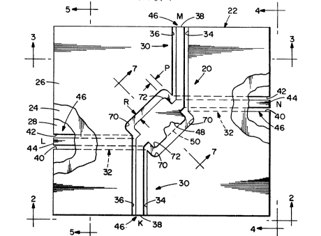
Fig. l is a plan view of a circuit board incorporating
the hybrid coupler of the invention;
Fig. 2 is a side elevation view of the circuit board,
taken along the line 2-2 of Fig. l;
Fig. 3 is a sectional view of the circuit board, taken
along the line 3-3 in Fig. 1;
Fig. 4 is a side elevations view of the circuit board,
taken along the line 4-4 in Fig. l;
Fig. 5 is a sectional view of the circuit board, taken
along the line 5-5 in Fig. 1;
Fig. 6 is a plan view of the reverse side of the circuit
board, taken along the line 6-6 in Fig. ~;
Fig. 7 is a fragmentary sectional view of the circuit
board, taken along the line 7-7 in Fig. 1; and
Fig. 8 is a schematic drawing of coplanar waveguides of
differing dimensions to demonstrate coupling between
coplanar waveguides on opposite sides of a circuit
board.
~. ~
7 1 3 1 6 2 2 3
DETAILED DESCRIPTION
With reference to Figs. 1-7, a microwave coupler 20 of
the invention is constructed on a circuit board 22. The
board 22 comprises a dielectric, electrically-insulating
substrate 24, and top and bottom metallic, electrically-
conductive sheets 26 and 28 disposed respectively on top
and bottom surfaces of the substrate 24. The substrate
24 may be formed of a blend of glass fibers and a
fluorinated hydrocarbon, such as Teflon,TM providing a
lo dielectric constant of approximately 2.2. Typically,
the metal used in the construction of the sheets 26 and
28 is copper. The terms "top" and "bottom" facilitate
description of the invention by relating the orientation
of the circuit board components to the arrangement shown
in the drawing, and are not intended to describe the
actual orientation of a physical embodiment of the
circuit board which, in practice, may be oriented on its
side or upside down.
Coplanar transmission lines, namely, waveguides 30 and
32 are formed respectively within the top and bottom
sheets 26 and 28. Each of the waveguides 30 and 32 is
formed by photolithographic techniques employing an
etching of a pair of slots to define a strip conductor.
In the waveguide 30, slots 34 and 36 define a strip
conductor 38. In the waveguide 32, slots 40 and 42
define a strip conductor 44. The slots 34 and 36 in the
waveguide 30, and the slots 40 and 42 in the waveguide
1 31 622~
1 32 are spaced relatively close together and are
parallel to each other to define ports 46 of the
coupler 20. Individual ones of the ports 46 are
identified further by the legends K, L, M, and N. At
the coupler 20, the spacing between the slots 34 and 36
is enlarged to form a top pad 48 in the top sheet 26.
Similarly, at the coupler 20, the spacing between the
slots 40 and 42 is enlarged to form a bottom pad 50 in
the bottom sheet 28. The widths of the slots 34 and 36
are increased at the periphery of the pad 48 so as to
retain the same ratio between slot width and strip
conductor width at the pad 48 as at the ports 46,
thereby to retain the same characteristic impedance of
the waveguide 30 at the pad 48. Similarly, the slots
40 and 42 are enlarged at the periphery of the bottom
pad 50 to retain the same ratio of slot width to strip
conductor width at the pad 50 as at the ports 46 to
retain the same value of characteristic impedance of
the waveguide 32 at the pad 50.
Fig. 8 is a diagrammatic representation of an end view
of a circuit board 52 having the same configuration as
the circuit board 22 (Fig. 1), and being formed of a
: dielectric substrate 54 clad on top and bottom surfaces
: 25 with metallic sheets 56 and 58. Four transmission
lines in the form of coplanar waveguides 60, 62, 64
and 66 are shown on the board 52. The waveguides 60
and 62 have a relatively narrow cross section, and are
disposed respectively in the top and the bottom sheets
56 and 58. The two waveguides 64 and 66 are of
relatively broad cross-sectional dimensions, and are
disposed, respectively, in the top and the bottom
- sheets 56 and 58. An electromagnetic wave is shown
13162~3
1 propagating in each of the waveguides 60-66, the
electromagnetic waves being indicated by an electric
field, identified by the legend E and portrayed as a
solid line, and a magnetic field, identified by the
legend H and portrayed by a dashed line. In the
narrow configuration of the waveguide 60 and 62, the
fringing fields are retained close to the waveguide,
while in the wider waveguides 64 and 66, the fringing
fields extend further into the substrate 54 so as to
allow for circulation of the magnetic field about the
center strip conductors of the two waveguides 64 and
66. By analogy with the coupler 20 of Fig. 1, the
narrow waveguides 60 and 62 represent the
configurations of either of the waveguides 30 and 32 at
a port 46. The widened configuration of the waveguides
64 and 66 represent the widened portions of the
waveguides 30 and 32 at the pads 48 and 50. Thereby,
it may be appreciated that the construction of the pads
48 and 50 introduces a significant increase in the
amount of coupling between the waveguides 30 and 32.
Furthermore, as a further feature of the invention, in
order to reduce coupling between the waveguides 30 and
32 at a distance from the coupler 20, the waveguides 30
and 32 are angled away from a center line 68 (Fig. 6)
of the pads 48 and 50 to increase the distance between
the waveguides 30 and 32. A typical value of the
angulation is 45 degrees. The length of each of the
pads 48 and 50 is approximately one-quarter wavelength,
namely the guide wavelength, as measured along the
center line 68, of the electromagnetic radiation
propagating along the waveguides 30 and 32. The width
of each of the pads 48 and 50 is less than the length
1 3t 6223
1 of the pads. The pads are shcwn as rectangular in
shape with the corners of the pads being rounded, and
similarly the contiguous portions of the slots 34, 36,
40, and g2 may have rounded corners, if desired, to
minimize reflections of electromagnetic signals
propagating in the waveguides 30 and 32. The
maintenance of a constant characteristic impedance
throughout the waveguide 30 and its pad 48, as well as
throughout the waveguide 32 and its pad 50, ensure a
smooth flow of power with no more than a negligible
amount of reflected power.
In the operation of the coupler 20, electromagnetic
signals entering the coupler 20 via port K propagate
past the pad 48 wherein a portion of the signal power
is coupled out, the remaining portion of the signal
continuing through the coupler 20 to exit by the port
M. The portion of the signal coupled by the coupler 20
exits via the port L. The port N is an isolation port
for signals entering via port K. It is noted that the
construction of the coupler 20 is symmetrical, and that
the transmission characteristic are reciprocal so that
any one of the four ports 46 may serve as an input
port.
A preferred embodiment of the invention has been
constructed to operate as a frequency of 3 ~Hz
(gigahertz). In this embodiment of the invention, the
board 22 of Fig. 1 has a square shape and measures 2.5
inches on a side. The top and bottom sheets 26 and 28
are each made of copper to a thickness of 3 mils. The
characteristic impedance of the waveguides 30 and 32
is 50 ohms. The dielectric constant of the substrate
131622'~
11
1 24 is 2.2. At a -3 dB coupling ratio, the bandwidth is
greater than 10 percent. The width of each slot 34,
36, 40 and 42 is 20 mils at the sites of the ports 46,
and is enlarged to a width of 85 mils, dimension P, at
S the ends of the pads 48 and 50, the slot widths being
widened to 71 mils, dimension R , at the sides of the
pads 48 and 50. The width of each of the pads 48 and
50 is 306 mils. The length of each of the pads 48 and
is 684 mils. The width of each of the strip
conductors 38 and 44 is 240 mils. The four outer
corners 70 of the circumferential slot about the pads
48 and 50 are rounded to a radius of 250 mils. Th~
four outer corners 72 of the pads 48 and 50 are rounded
with a radius of 64 mils. The substrate 24 has a
thickness of 58 mils. If desired, the bandwidth can be
decreased by raising the dielectric constant of the
substrate 24 as by use of alumina, for example.
The foregoing construction of the coupler 20 provides
for the desired capability of the invention to couple a
desired fraction of input electromagnetic power from a
transmission line on one side of a circuit board to a
transmission line on the opposite side of the circuit
board. The electrical characteristics of the coupler
~0 are that of a quadrature hybrid coupler wherein
power inputted at port K is outputted partly at port M
with essentially zero phase shift and partly at port L
with a phase shift of +90 degrees. Essentially no
power is outputted at port N; however, in the event
that there were reflection at a load coupled to port L,
such reflected power would exit partly at port N with
the balance exiting at port K.
13l62~
1 It is to be understood that the above described
embodiment of the invention is illustrative only, and
that modifications thereof may occur to those skilled
in the art. Accordingly, this invention is not to be
regarded as limited to the embodiment disclosed herein,
but is to be limited only as defined by the appended
claims.
'''~,