Note: Descriptions are shown in the official language in which they were submitted.
~ TI~2003A1
1 31 S2J~
This invention relates to digital telecommunication networks and more
particularly to cross-connect modules for (1) cross-connecting digital
telecommunication circuits and for ( 2 ) monitoring, testing, restoring and
repairing such circuits.
Digital signal cross-connect equipment plays a very vital role in the
installation, monitoring, testing, restoring and repairing digital
telecommunication networks. Digital si~nal cross-connect modules are
frequently used in digital networks to provide a central cross-connect
location that is convenient for testing, monitoring, restoring and repairing
the digital lines and associated telecommunication equipment. The digital
cross-connect modules provide temporary jack access to the digital signals
to monitor the signals and to test and repair the digital circuits and
equipment. Digital signal cross-connect modules are most frequently used
in both large and small telephony central offices, remote sites and
customer premises. It is necessary that with respect to the remainder of
the network, the digital signal cross-connect module must appear
transparent. This is particularly true and more critical when dealing with
digital signals that are transmitting at line rates in excess of 40 million
bites per second (Mbps).
Prior to the applicant's invention, the digital signal cross-connect
module illustrated in Figs. 1 and 2 has been utilized. It is helpful in
understanding, the applicant's invention to be familiar with the module
illustrated in Figs. 1 and 2. Specifically the module (Fig. 1) is identified
generally with the numeral 10 having a case or housing 12. The module 10
includes a front panel 14 that is spaced from a back panel 15. The
module 10 has an input jack 16, an output jack 18 and a monitor jack 20
on the front panel for receiving patch cord plugs.
TE2003Al
1 31 6233
The module 10 includes an input connector 22, an output
connector 24, a cross-connect input connector 26 and cross-connect output
connector 28 that are all mounted on the back panel 15.
The module 10 (Fig. 2) includes an input jack switch 30 that is
electrically connected to the input jack 16. An output jack switch 32 is
electrically connected to the output jack 18. The module 10 includes an
internal input coaxial cable 34 that extends from the input jack 16 to the
input connector 22. An output coaxial cable 36 extends from the output
jack 18 to the output connector 24. A cross-connect branch input coaxial
1 0 cable 38 extends from the cross-connect input conductor 26 to the input
jack switch 30. A cross-connect branch output coaxial cable 40 extends
from the cross-connect output connector 28 to the output jack switch 32 as
illustrated in Fig. 2. A monitor cable 42 extends from the monitor jack 20
to the output coaxial cable 36 for monitoring the digital signals on the
output coaxial cable 36.
Although the module 10 has operated satisfactorily, it has many
limitations which are overcome by the applicant's invention. The
applicant's invention as described as follows is considered to be more
versatile and has many advantages that will become apparent upon reading
the following detailed description.
Fig. 1 is an illustration of a prior art digital cross-connect module in
which its electrical circuit is illustrated schematically in Fig. 2.
` ` A preferred embodiment of the applicant's invention is illustrated in
the following figures, in which:
2 5 Fig . 3 is a perspective front view of a preferred embodiment,
emphasizing a front panel of the module illustrating the locations of front
panel jacks;
-~ TE2003Al
1 31 6233
Fig. 4 is a rear perspective view of the module illustrated in Fig. 1
which emphasizes coaxial connectors on a back panel of the module;
Fig. 5 is a side view of the module illustrated in Figs. 3 and 4 with a
side panel removed to illustrate the interior of the module housing;
Fig. 6 is an electrical schematic view of the module illustrated in
Figs. 3-5;
Fig. 7 is a cross-sectional view taken along line 7-7 in Fig. 5;
Fig. 8 is a fragmentary side view of a portion of the module
illustrating a monitor jack and monitor cable;
Fig. 9 is a fragmentary cross-section of a jack switch incorporated
within the module illustrating the switch with two contacts in the closed
position;
Fig. 10 is a fragmentary side view similar to Fig. 9 exeept showing a
portion of the switeh removed to illustrate a number of internal
15 components;
Fig. 11 is a fragmentary eross-seetion of view taken along line 11-11
in Fig. 9;
Fig. 12 is a fragmentary side view similar to Fig. 10 except showing
one of the contacts in an open, grounded position in response to the
20 insertion of a plug into a respective jaek;
Fig. 13 is an electrical schematic of a portion of the module
illustrating one switch contact in a closed position and the other in an
open, grounded position;
Fig. 14 is a fragmentary side view similar to Fig. 12 exeept showing
25 the second switch in an open, grounded position; and
Fig. 15 is an electrical schematic similar to Fig. 13 except illustrating
both switches in an open, grounded position.
1 3 1 6 2 3 3 TE2003A1
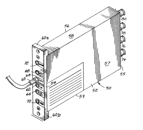
Referring now to the drawings, as illustrated in the Figs. 3-5, a
difital cross-connect module generally designated with the numeral 50 for
interconnecting or cross-connecting equipment in a telecommunication
network, at a remote location. The module provides a central access
5 location to the equipment for facilitating installation, monitoring, testing,
restoration and repair of the telecommunication equipment. A single
module 50 generally interconnects two items of telecommunication equipment
of the digital telecommunications network in a noncross-connected state.
The module 50 is included in a rack or bank of similar modules forming a
10 digital signal cross-connect terminal unit. Most frequently the terminal
unit is mounted in bays at a convenient central location in large or small
central telephone offices or remote sites or at the customer premises. The
module 50 is able to appear transparent to the digital telecommunication
network that i~ capable of transmitting digital information at a high rate in
excess of 40 million bits per second (Mbps), particularly DS-3 at 44.736
Mbps and DS-4 at 272.176 Mbps.
The module 50 includes a slender housing or case 52 that is mounted
upright as illustrated in Figs. 3 and 4. The housing 52 provides a
.:.. .
` RF-EMI shield to prevent RF energy from interfering with the transmission
2 0 of the difital signals .
The housing 52 (Fig. 3) includes a front panel 54 that is elongated in
the vertical dimension and narrow in the horizontal direction. The front
panel faces the front of the terminal unit and provides easy access to
enable telecommunication transmission enfineers, installers and repair
2 5 personnel to have convenient remote electrical access to the
telecommunication circuits and networks. The housing 52 (Fig. 4) includes
a back panel 55 that is elongated in the vertical direction and narrow in
the horizontal direction to provide a slim profile for the module 50. The
-_~ TE2003Al
1 31 6~33
back panel faces the rear of the terminal unit and provides limited access.
The housing 52 includes side walls 56 and 57 that extend between the
front panel 54 and the back panel 55. The housing 52 includes a top
wall 58 and a bottom wall 59. The front panel 54 has front panel
flanges 60a and 60b that respectively extends upward and downward to
facilitate the mounting of the module 50 to the digital signal cross-connect
terminal unit or rack. In relatively large and small central telephone
offices, the modules 50 are mounted in a plurality of vertical spaced rows
forming racks of cross-connect modules.
The module 50 (Figs. 3 and 6) includes an input jack 62, an output
jack 64, a cross-connect input jack 66 and a cross-connect output jack 68.
The jacks 62, 64, 66, 68 are mounted in the front panel 54 in a generally
horizontal parallel relationship with each of the jacks having an opening to
receive a plug 69 of a patch cord or a looping plug which is generally
1 5 used for the purpose of installation, monitoring, testing, restoring or
repairing of the digital telecommunication network circuits (equipment).
In a preferred embodiment, the jacks 62, 64, 66, and 68, as shown in
Fig. 3, are evenly spaced with respect to each other at a desired interval
commensurate with the axial spacing of a looping plug so that a looping
2 0 plug may simultaneously be inserted (1) in the input jack 62 and the
output jack 64, or (2~ in the input jack 62 and the cross-connect input
jack 66, or (3) the output jack 64 and the cross-connect output jack 68.
The input jack 62 is mounted intermediate and evenly spaced from the
output jack 64 and the input cross-connect jack 66. The output jack 64 is
positioned intermediate the input jack 62 and the cross-connect output
jack 68. More specifically, the input jack 62 is mounted immediately above
the cross-connect input jack 66. The output jack 64 is mounted
immediately above the input jack 62. The cross-connect output jack 68 is
1 3 1 6 ~ 3 3 TE2003A1
mounted immediately above the output jack 64. The parallel relationship of
the jacks 62, 64, 66 and 68 is illustrated more specifically in Fig. 5. An
electrical schematic of the module 50 is illustrated in Fig. 6.
The module 50 also includes a bottom input monitoring jack 70 and a
5 top output monitoring jack 72 that are likewise mounted in the front
panel 54. The input monitoring jack 70 is preferably mounted below the
cross-connect input jack 66. The output monitoring jack 72 is preferably
mounted above the cross-connect output jack 68.
The module 50 (Fig. 4) further includes an input connector 74, an
10 output connector 76, a cross-connect input connector 78 and a
cross-connect output connector 80. Each of the connectors 74, 76, 78,
and 80 are mounted in the back panel 55 as illustrated in Figs. 4 and 5.
The connectors 74, 76, 78 and 80 are preferably BNC or TNC coaxial
connectors frequently referred to as installer connectors. The
connectors 74, 76, 78 and 80 are respectively connected to the digital
signal lines or equipment in which the input connector 74 is connected to a
digital signal input portion of a first line or first item of equipment of a
telecommunication network (not shown). The output connector 76 is
connected to the output portion of the first line or unit of equipment (not
2 0 shown ) . The cross-connect input connector 78 is connected to the input
portion of a second line or second piece of telecommunication equipment
(not shown). The cross-connect output connector 80 is connected to an
output portion of the second line or piece of telecommunication equipment
(not shown). Coaxial cables (not shown) are most frequently used to
25 connect the telecommunication equipment to the module connectors 74, 76,
78 and 80. Frequently the coaxial cables are placed and supported in
trays that extend generally horizontally along the back panels 55.
1 31 6 ~ 33 TE2003Al
Generally once the connectors 74, 76, 78 and 80 are hooked up it is
seldom that they are disconnected. For the purpose of this invention, it
will be considered that the connectors 74, 76, 78 and 80 are of a
permanent connection although it is recognized that the connectors 74, 76,
5 78 and 80 may be disconnected from the telecommunication equipment when
the equipment is rearranged, disassembled and the like.
The module 50 (Figs. 5 and 6) further includes an input coaxial
conductor 82, an output coaxial conductor 84, a cross-connect input
conductor 86 and a cross-connect output conductor 88. The input coaxial
conductor 82 has ends 82_ and 82b that permanently interconnect the input
coaxial conductor 82 between the input jack 62 and the input connector 74.
The output coaxial conductor 84 has one end 84a permanently connected to
the output jack 64 and the other end 84b is permanently connected to the
output connector 76. The cross-connect input conductor 86 has end 86a
1 5 permanently connected to the cross-connect input jack 66 and another
end 86b permanently connected to the cross-connect input connector 78.
The cross-connect output conductor 88 has end 88a permanently connected
to the cross-connect output jack 68 and another end 88b permanently
connected to the cross-connect output connector 80.
The module 50 (Figs. 5 and 6) further includes an input switch
assembly 90 and an output switch assembly 92. Rach of the switch
assemblies are aligned along parallel axes as illustrated in Fig. 5. As
illustrated schematically in Fig. 6, each of the switch assemblies 90, 92
include a unitary conductive bridge member generally designated with the
numeral 94 for normally cross-connecting conductor 82 with conductor 86
and cross-connecting output coaxial conductor 84 with cross-connect
coaxial output conductor 88, respectively. When a plug 69 is inserted into
any one of the jacks 62, 64, 66 or 68, the associated switch, in response
~ TE2003Al
1 31 ~233
to such insertion, disconnects the respective conductor 82, 84, 86 or 88 to
isolate the conductor and associated equipment from the cross-connect
circuit. The switch assemblies 9û, 92 will be explained in more detail in
the following paragraphs.
Each of the jacks 62, 64, 66 and 68 (Figs. 9-12) includes a hollow or
peripheral outer cylinder 100 for receiving a barrel of the plug 69 therein.
Each of such jacks has an open forward end or plug entry sleeve 103 that
is mounted in the front panel 54 for receiving a plug. Each jack has a
closed rear end 104 that is connected to a respective coaxial conductor. A
1 0 flange 105 is affixed on the forward end 103 for mounting the jack firmly
to the front panel 54. Each of such jacks has a central cavity 106 for
receiving a plug 69. Each of such jacks has a central or axial conductor
member 107 that projects forward from the rear end 103 for receiving a
plug pin. The central conductor member 107 is supported in a central
insulative support 109 at the rear end 103.
Each of the input and output monitoring jacks 70 and 72 (Fig. 8)
include a flange 112 that mounts the monitoring jack to the front panel 54.
A separate monitoring coaxial cable 113 extends from each of the
monitoring jacks 70, 72 to the input coaxial conductor 82 or output coaxial
2 0 conductor 84, illustrated schematically in Fig. 6. The cable 113 includes
an outer coaxial conductor 114 that engages and is in contact with an
outer conductor of the coaxial conductors 82 or 84. Each of the
monitoring coaxial cables 113 (Fig. 8) includes an inner conductor 116 that
is connected in series to an isolation resistor 118. One lead 120 of the
resistor 118 is connected to the inner conductor 116 and another end 122
is connected to a central conductor of the coaxial conductors 82 or 84.
The lead 122 extends through an aperture 124 formed in the outer braided
portion of the coaxial cable. The other lead 122 then extends through a
1 3 1 6 2 3 3 TE2003A1
slit 124 formed in the coaxial insulator. The terminal end of lead 122 is
affixed to the inner conductor by spot weld 127.
As illustrated in Fig. 7, each of the four connectors 74, 76, 78 and
80 includes a threaded housing 130 that extends from a rear end 132 to a
forward end 134 projecting from the back panel 55. Each of the
connectors has a central metal female sleeve 136 that is supported by a
rather cylindrical block 138 within the housing 130.
Referring to Fig. 5, input switch assembly 90 has a switch axis 140
and output switch assembly 92 has a switch axis 142. Each of the switch
assemblies 90, 92 have a unifying housing 144 (Figs. 5, 9-12) that
encircles the outer cylinder 100 of two of the jacks 62 and 66 or 68 and
64. Each of the housings 144 has an interior insulative support block 146
mounted therein in which the support block is illustrated in Fig. 11 having
upper and lower symmetrical block parts 146a and 146b that form a central
cavity 148 therein. The cavity 148 (Fig. 10) has a side opening facing
central conductor 107_ of one of the two jacks and a second opening facing
the other central conductor 107b of the other jack. The insulative support
block 146 fits in a receiving slot 152 that is aligned along the switch
assembly axis.
Each of the switch bridge members 94 (Fig. 6) includes a unitary,
generally V-shaped, conductive spring 158 that has an apex 160 that is
mounted in the receiving slot 152. The V-shaped conductive spring 158
has a contact arm 162 that extends outward from one side of the cavity 148
to contact conductor 107_ and a contact arm 164 that extends outward from
the other side of the cavity 148 to contact conductor 107b. Each of the
contact arms 162, 164 extends outward from the apex 160 to a curved end.
Each of the bridge members 94 (Fig. 9) includes a insulative
bumper 170a and 170b mounted on respective switch arms 162, 164 for
1 3 1 ~ ~ 3 3 TE2003A1
receiving and being engaged by the end of the plug 69, as illustrated in
Fig. 12, for deflecting the respective contact arm 162, 164 away from the
central conductor 107a, 107b to disconnect the associated equipment from
the cross-connect circuit. The contact arms 162, 164 are biased outward
S for normally engaging the central conductor 107a, 107b and are deflected
from such normal engagement or contact by the insertion of the plug 69.
An arm stop 172 (Figs. 10-12) is mounted within the central
cavity 148 and aligned on the switch axis. The arm stop 172, as
illustrated in Fig. 12, limits the inward movement of the contact arm 162 or
164 when a plug 69 is inserted into a respective jack. The arm stop 172
prevents overtravel of the arms 162, 164. The arm stop 172 is engaged
by the insulative bumper 170_ and 170b.
The switch assembly further includes a grounding post 174 that is
mounted in the central cavity 148 aligned along the switch housing axis.
The grounding post 174 includes a contact button body that has an arcuate
surface that is engaged by the contact arms 162, 164 as illustrated in
Fig, 12 when a plug is inserted into a respective jack. The arcuate
surface of the grounding post 174 is capable of engaging one or both of
the arms should plugs 69 be inserted in both of the respective jacks
(Fig. 14).
The grounding post 174 (Figs. 11 & 12) has a cavity formed therein
receiving a grounding resistor 182. The grounding resistor 182 is
positioned along the axis of the switch assembly. One lead of the
grounding resistor 182 is connected to the grounding post 174 and the
opposite lead is connected to the switch housing for grounding the
grounding post 174.
_~ TE2003A1
~ ~ 1 S~33
It should be noted that the module 50 enables monitoring of either the
input signals or output signals or both, via the monitoring jacks 70 and 72
tFigs. 3 ~ 5) without interfering with signals on the respective lines.
Furthermore, it should be appreciated that the module 50 enables the
S installer, tester, monitor or repair person to utilize a patch cord to isolate
any one of conductors 74, 76, 78 and 80 and reroute the line temporarily
to connect at a different module. The module 50 greatly increases the
ability of the transmission engineer and his staff to detect problems or
abnormalities and to isolate the abnormality and to make a proper repair.
10 Furthermore, the module 50 provides a cross-connection capability at the
front panel. Purthermore, it enables looping plugs to be utilized for
testing the circuits by rerouting the circuits directly from the front panel.
Furthermore, the module 50 has a unique switch structure that reduces the
amount of digital infnrmation that is lost in transition from a cross-connect
15 condition to a patch condition. It is found that the module 50 enables the
restoration of jack service in less than five seconds.
11