Note: Descriptions are shown in the official language in which they were submitted.
` 13162~5
1 74424-31
SHIELDED ENCLOSURE
Field of the Invention
The present invention relates to shielded enclosures for
alternating current electronic circuits.
Backaround of the Invention
It is known in the art to shield circuitry which
operates at high frequencies to prevent high-frequency radiation
from interfering with other circuits. Shielding is accomplished
by surrounding the circuitry with metal shielded enclosures, as
disclosed, e.g., in U.S. Patent No. 4,658,439.
In shielded enclosures, it may be desirable to provide
good electrical connection between two members of the enclosure
(e.g., a wall member and a cover) by having them mate at flat,
smooth surfaces that are bolted up against each other around the
junction between the two. Gaps in the shielded enclosure (e.g.,
at a junction), which limit the shielding effectiveness, can be
blocked by providing a conductive, compressible gasket material in
a precision groove formed in one member.
Summarv of the Invention
It has been discovered that, by providing a geniculated
(i.e., abrupt angle) junction between first and second storage
members that together make up an enclosure for electronic devices,
transmission of alternating current radiation from the devices can
be advantageously inhibited.
The invention provides a shielded enclosure assembly
comprising devices utilizing high frequency alternating current
signals and generating alternating current radiation, a first
storage member having a first surface and a second surface, a
B
131~2~
la 74424-31
second storage member having a third surface mating with said
first surface and a fourth surface mating with said second
s~rface, and a plurality of connector elements uniformly
positioned around the periphery of said first storage member to
secure said first storage member to said second storage member and
to provide intimate contact between the two, said intimate contact
having a spacing that is determined by surface roughness of said
first surface and said third surface, said enclosure surrounding
said devices, said first and second surfaces forming a geniculate
junction with said third and fourth surfaces, said geniculate
junction and said spacing serving to inhibit transmission of said
alternating current radiation from said devices.
In preferred embodiments the first storage member is a
top cover, and the second storage member is a wall member; the
wall member has a recess for receiving the cover; the cover and
wall member mate at opposing flat surfaces; the cover is secured
to the wall
--2--
member via a plurality of connector elements (e.g.,
bolts) between the two around the junction; there is a
second recess on the wall member and a mating bottom
cover; the wall member has an interior lip for
supporting a circuit board; and there are holes in the
wall member for receiving electrical connectors.
Other advantages and features of the invention
will be apparent from the following description of a
preferred embodiment thereof and from the claims.
Description of the Preferred Embodiment
The preferred embodiment will now be described.
Drawinqs
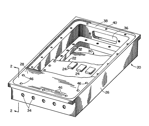
Fig. 1 is a perspective view of a shielded
enclosure according to the invention.
Fig. 2 is a partial sectional view, taken at
2-2 of Fig. 1.
Fig. 3 is a plan view of a wall member of the
Fig. 1 enclosure.
Fig. 4 is a side elevation of the Fig. 3 wall
member.
Fig. 5 is a front eleva~ion of the Fig. 3 wall
member.
Fig. 6 is a rear elévat'ion of the Fig. 3 wa~l
member.
Structure
Referring to the figures, shielded enclosure 20
completely surrounds electronic printed circuit board 22
having high-frequency, electronic devices 24 thereon.
Shielded enclosure 20 includes wall member 26, top cover
28, and bottom cover 30, all made of aluminimum.
Wall member 26 includes lip 32 on which
electronic printed circuit board 22 is bolted. Wall
member 26 also has coaxial connector holes 34 and
D-connector hole 36 into which coaxial connectors (not
( ` ~ -3- 1~162~
shown) and a filtered D-connector (not shown~ are placed
respectively. These electrical connectors are used to
allow signals to be transmitted to and received from the
electronic circuitry within enclosure 20 while
preventing high-frequency radiation from escaping from
enclosure 20.
Wall member 26 has surface 38 (about 0.42 inch
wide along the longer side and about 0.47 inch wide
along the shorter side) and perpendicular surface 40
(0.10 inch high), which together define a recess into
which top cover 28 is received. Referring to Fig. 2,
top cover 28 includes surface 42 and edge surface 44,
which correspond to and mate with surfaces 38 and 40 of
wall member 26. Wall member 26 and top cover 28 are
made of cast aluminimum and are "tumbled" in sand or
glass to provide polishing of surfaces. The casting
process provides very flat surfaces 38, 42, permitting
intimate contact of the two. Surface roughness is less
than or equal to 63 microinches RMS. Surfaces 38, 42
are treated to provide good electrical conduction
between them; in particular, the surfaces are degreased,
caustic etched 0.0015" max and aluminum phosphate
treated per MIL-C-10578D, Type fII.
Cover 28 is tightly secured to wall member 26
via screws 46 around the periphery of cover 28, thereby
providing good electrical connection between the two.
Because of the flatness of surfaces 38, 42, the spacing
between them is determined by surface roughness. The
gap (i.e., on both sides) between surfaces 40, 44 is
30 between 0.035" and 0.070". Wall member 26 includes a
similar recess into which bottom cover 30 fits and is
secured by a plurality of screws (not shown). The total
gap between the side surfaces of bottom cover 30 and the
4~
opposing surfaces of the mating recess is between 0.055"
and 0.062". The junctions between wall members 26 and
recessed covers 28, 30 are geniculated, i.e., have
abrupt (in particular 90) angles.
Enclosure 20 thus includes a first storage
member (top cover 28) with first (42) and second (44)
surfaces, a second storage member (wall member 26) with
third (38) and fourth (40) surfaces that mate with the
first and second surfaces, and a third storage member
(bottom cover 30) that fits in a recess at the bottom of
the second storage member defined by fifth and sixth
surfaces. The bottom cover has seventh and eighth
surfaces that mate with the fifth and sixth surfaces.
OPeration
Shielded enclosure 20 is used in automatic test
equipment to enclose a high-frequency alternating
current instrument. The bolting of printed circuit
board 22 on lip 32 provides a good ground path for the
electronic components. The only gaps on enclosure 20
are those at the geniculated junctions between wall
member 26 and recessed covers 28, 30. The abrupt angle
(preferably 90 or less) acts to! inhibit high-frequency
radiation from escaping from enclosure 20, as do the
small gap between surfaces 38, 42 (determined by the
roughness) and the small gap between surfaces 40, 44
(determined by the tolerances of covers 28, 30 and the
recess on wall member 26). The geniculated junctions of
enclosure 20 are designed to inhibit high freguency
radiation in the range 1 megahertz to 10 gigahertz from
escaping from shielded enclosure 20. Enclosure 20 has
advantages over the prior use of gaskets in avoiding the
cost of the gasket material, the precision machined
i31~2~5
74424-31
groove and labor, and in avoiding the loss of gasket effectiveness
after multiple compressions
Other Embodiments
Other embodiments of the invention are within the scope
of the following claims, E.g. t the junction between the wall
member recess and the corresponding cover may have a plurality of
abrupt angles in it to provide increased shielding over a single
abrupt angle. As the frequencies of signals to be inhibited
increase, or as the desired shielding effectiveness increasest the
gaps will have to be made smaller and/or the number of abrupt
angles will have to be increased in order to restrict the passage
at the junction and effectively inhibit transmission of the
alternating current radiation from the electronic devices- Alsot
other conductive materials such as brass or copper could be used
in place of aluminum.