Note: Descriptions are shown in the official language in which they were submitted.
131627.'
M 975-1 1989-05-22
Thermistor intended Primarily for temperatuIe measurement and
~rocedure for mRnufacture of a thermistor
Technical field of the invention
The present invention relates to a thermistor, primarily
intended for temperature measurement. The thermistor is
simple in its design and construction, and is inexpensive to
produce. The design of the thermistor allows effective
trimming, to give readings of great precision. These
characteristics make the thermistor according to the invention
particularly suitable for use in disposa~le products, such as
disposable medical thermometers.
The invention also relates to a procedure for the manufacture
of a thermistor.
Backqround of the invention
A thermistor is a semiconductor, the resistive properties of
which vary with the temperature. In order to enable the
resistive properties of the thermistor to be utilized, it is
provided with contacts that can be connected to an electric
circuit. The resistance and temperature sensitivity of the
thermistor are determined by the composition of the material
of the semiconductor, the physical dimensions of the active
substance of the thermistor, and the temperature.
The fact that the resistance depends on the physical
dimensions of the material of the thermistor makes it possible
to regulate the ohmic value of the thermistor by removing or
trimming off some of the material. The resistance of the
thermistor is also determined by the area of the contact
surfaces on the thermistor material, which means that the
ohmic value of the thermistor can be adjusted by removing or
.
2 1 31 6272
trimming off some of the contact surface on the material of
the thermistor.
Different types of thermistor are known. In GB-A-1470630 a
thermistor produced by a thick-film process is described. A
first layer of contact material is applied to a substrate
plate by screen printing, forming a number of pairs of
electrodes. After firing, a second layer of thermistor
material is printed on the first, to form a thermistor plate
over the pair of electrodes. After refiring, the thermistor
is trimmed by having part of the material removed with the aid
of a laser. The substrate plate is divided into discrete
thermistor elements and encapsulated in a protective layer of
suitable material.
GB-A-1287930 describes a thermistor consisting of a first
layer of contact material, a second layer of thermistor
material fully encapsulating the first layer, and two
electrode surfaces arranged parallel on the thermistor layer.
GB-A-1226789 shows a similar thermistor arranged on a
substrate plate, which consists of a thermistor plate between
a lower and an upper electrode surface. The electrode
surfaces are extended in opposite directions on the substrate
plate, in order to form contact surfaces for connection to an
electric circuit.
None of the thermistors previously known is designed to be
simply and very flexibly adaptable to different spheres of use
while maintaining the possibility of high precision with the
aid of exact trimming. This is essential to the production
and ~rimming of the thermistors at a low enough cost for them
to be usable as disposable products, such as disposable
thermometers.
Summary o~ the invention
The object of the present invention is thus to produce a
1 3 1 6 2 7 !_
thermistor specifically designed for temperature measurement
and suitable for disposable use, while possessing high
accuracy and flexibility of application.
The thermistor must therefore be possible to produce very
efficiently with a high degree of automation and high rate of
production, despite the strict requirement for accuracy. The
absolute resistance of the thermistor must be capable of very
flexible modification in order to enable the thermistors to
work within different temperature ranges while retaining the
same rational production method and trimming procedure.
The present invention accomplishes these purposes by the
design of a thermistor which is characterized by the fact that
it comprises at least two thermistor plates on a carrier
adjacent to each other and connected in series, said plates
are separated from each other by a preferably elongated gap,
and the upper surfaces of said plates are largely covered with
upper electrode surfaces, the thermistor plates being arranged
within a limited area of the carrier so that the maximum
aggregate area of the thermistor plates is constant, whereas
the size of each individual thermistor surface is variable by
displacement of the position of the gap(s) within the said
limited area on the carrier, for adjustment of the total
resistance of the thermistors to different values.
The process by which the thermistor is manufactured is
according to the invention characterized by the fact that the
thermistor is manufactured by a thick-film process, by
screen printing on a limited area of a carrier a first layer
of contact material to form one or more lower electrode
surfaces, a second layer of thermistor material to form
thermistor plates arranged on the lower electrode surfaces and
separated from one another by a preferably elongated gap, and
a third layer of contact material to form one or more upper
electrode surfaces which largely cover the thermistor plates,
said upper electrode surfaces are trimmed to a predetermined
resistance value.
1 31 6212
Further advantageous features of the invention will be
apparent from the following description of embodiments of the
invention, and from the dependent claims.
The design of the thermistor with two or more thermistor
plates separated by a gap and connected in series within a
limited area on the carrier implies the advantage that the
total resistance of the thermistor can be altered from a very
high maximum value to a low minimum value simply by altering
the position of the gap(s) on the carrier. The part-
resistance of each thermistor plate is inversely proportional
to the area, and the total resistance of the thermistor is the
sum of the part-resistances of the thermistor plates connected
in series. The greater the difference in size between the
thermistor plates, i.e. the further out towards the edges of
the limited area the gap is placed, the higher the total ohmic
value of the thermistor. The lowest ohmic value is obtained
when the thermistor plates are egual in size. A further
increase in the total resistance may be achieved by giving the
thermistor more than two thermistor plates.
The size of the upper electrode surfaces is adjusted to the
size of the thermistor-plates, which means that irrespective
of the position of the gap or gaps on the carrier the
aggregate upper electrode surface is constant. This fact
means that the total area available for trimming remains
unaltered in spite of variations in the placing of the gap,
which makes it possible to use the same effective trimming
process for thermistors with different resistance performance.
The thermistor as defined in the claims can be used for
measurement of temperature within different temperature
ranges. These characteristics lend flexibility to the
thermistor and enable its field of application to be extended
by a simple change in the production process, for example by
changing the screen in a screen printing process, while
retaining the same effective production method and high
5 1 31 $~7~
accuracy.
Yet another advantage of the thermistor according to the
present invention is the possibility of selecting the upper
electrode surface(s) on which the thermistor is to be trimmed,
depending on the demanded accuracy of the thermistor. For
example, in a thermistor with two thermistor plates with upper
electrode surfaces of which one is larger than the other, the
effect of trimming the one surface will differ from the effect
of trimming the other, i.e. the percentage change in the
resistance varies depending on which surface is trimmed. ~f
the larger surface is trimmed, the precision will be greater.
When high precision is demanded, the smaller surface
preferably can be rough-trimmed and the larger surface can be
1~ fine-trimmed. When the smaller surface is trimmed, the speed
of trimming is instead increased, which means that a rough
trimming of the larger surface and fine trimming of the
smaller one gives quicker but less accurate trimming. Other
combinations of trimming are also possible within the scope of
the invention, such as only one trimming in one of the
surfaces or several tri~minqs in just one surface.
The connection of the thermistor to an electric circuit is
accomplished by connecting electric conductors direct to the
electrode surfaces or to special contact surfaces connected to
the electrode surfaces. The conductors may be connected in
various ways to the electrode surfaces/contact surfaces, such
as by gluing, soldering, bonding or by spring contact. The
special contact surfaces are extended so that they are not in
direct contact with the thermistor plates, which has the
advantage that it reduces the risk of heating of the material
of the thermistor and thus changing the properties of the
material when connecting the conductors by, for example,
soldering.
Brief descriPtion of the drawinqs
An embodiment of the present invention and modifications
6 t3l6272
thereof are described in greater detail below with reference
to appended drawings, where
- Fig. 1 shows a perspective view of a first embodiment of a
thermistor before trimming,
- Figs. 2 a-e show the different layers of the thermistor ~n
the embodiment according to Fig. 1,
.
- Fig. 3 shows a number of thermistors according to Fig. 1 on
a substrate plate,
- Fig. 4 a shows a second embodiment of the thermistor and
- Fig. 4 b shows a section of the thermistor according to Fig.
4 a,
- Figs. 5 a and b show in the same way as in Figs. 4 a and b
a third embodiment of the thermistor before it has been
provided with trimming cuts and a protective polymer layer,
- Figs. 6 a and b show in the same way as in Figs. 4 a and b
a fourth embodiment of the thermistor,
- Figs. 7 a and b show in the same way as in Figs. 4 a and b
a fifth embodiment of the thermistor without trimming cuts
and polymer layer.
Detailed description of preferred embodiments of the
invention
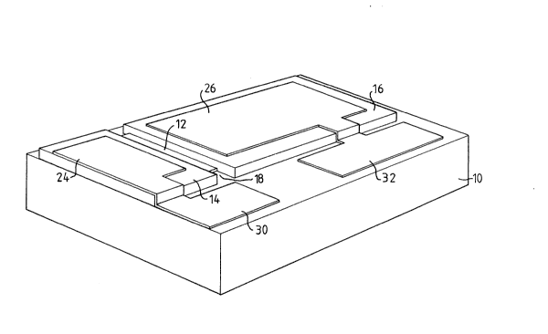
Fig. 1 shows a thermistor according to the invention, which is
preferably manufactured by a thick-film process. On a non-
conducting substrate plate (8), see Fig~ 3, preferably of
aluminium oxide, with notches for approx. 200 carriers (10),
a first layer of a conductive contact material is applied by a
screen printing process, forming a first electrode surface
- : . . . ................. ;, . - ,
.
7 1316272
(12) or bottom conductor on each carrier (10), which is shown
more clearly in Fig. 2 a.`The substrate plate is dried to
remove the solvent in the print, after which firing takes
place in a belt furnace.
'Fig. 2 b shows the carrier (10) with a second screen printed
layer of thermistor paste, which forms two separate thermistor
plates (14, 16) between which is formed an open gap (18).
The surface area of the thermistor plates (14, 16) is so
defined that the outer edges of the plates (20) lie outside
the outer edges (22) of the first-electrode surface, except
for the gap (18) between the plates. The substrate plate
with the two layers of contact and thermistor material is now
dried again.
Fig. 2 c (see also Fig. 1) shows how an additional layer of
conductive contact material has been screen printed on the
substrate plate so that a second electrode plate (24, 26) is
formed on each of the thermistor plates (14, 16), these
electrode surfaces forming the top conductor. These electrode
surfaces (24, 26) are so designed that their outer contours
(28) are inside the outer edges (20) of the thermistor plates
with the exception of a part of each electrode, which is
extended beyond the thermistor plate (14, 16) and there forms
a contact surface (30, 32) which is in direct contact with the
carrier (10).
In order to prevent short-circuiting between the electrode
surfaces, i.e. between bottom and top conductors, it is
essential for the top conductor (24, 26) to be smaller in area
than the thermistor plates (14, 16) and for the thermistor
plates (14, 16) to be larger than the bottom conductor (12).
The substrate plate is now dried again and then fired in a
belt furnace.
Adjustment of the resistances of the thermistors is
accomplished by trimming the upper electrode surfaces (24, 26) '
8 1 3~ 627~
of the thermistor, see Fig. 2 d. The trimming is preferably
carried out in two stages, a rough trimming and a fine
trimming. In the em~odiment of the thermistor shown in Figs.
1 and 2, a rough trimming (34) has been carried out in one
~24) of the two upper electrode surfaces, preferably in the
smaller one, and a fine trimming (36) has been carried out in
the other electrode surface (26), i.e. the larger.
Fig. 2 d shows how parts of the two upper electrode surfaces
have been removed by rough trimming (34) in the form of a
number of cuts and fine trimming (36) in the form of a number
of trimming holes.
After completion of the trimming the thermistor, except for ¦
the contact surfaces (30, 32), is coated with a polymer layer
(38) by a screen printing process, which helps to protect the
thermistor and in particular counteracts its ageing. The
protective polymer layer is shown in Fig. 2 e.
Figs. 4 a and 4 b show a thermistor with an alternative
embodiment of the placing of the contact surfaces (30, 32).
On the upper electrode surfaces (24, 26) there is an
insulating layer (40), in which there is an opening (42, 44)
to each of the two electrode surfaces (24, 26). On the
insulating layer, two contact surfaces (30, 32) are placed,
each on a thermistor plate l14, 16) with connections (46, 48)
through the openings t42, 44) to the electrode surfaces (24,
26). The trimming here is achieved by rough trimming (34) of
the larger electrode surface and fine trimming holes (36) in
the smaller electrode surface.
Figs. 5 a and b show an embodiment of the thermistor with more
than two, in fact four, thermistor plates. The carrier (10)
is provided with two lower electrode surfaces (12, 13) on
which four thermistor plates (14, 15, 16, 17) are arranged in
pairs. Three upper electrode surfaces (24, 25, 26) are
arranged on the thermistor plates, the two outermost (24, 26)
being connected to the two contact surfaces (30, 32). The
-, ; , , ~ -
t ~1 6~7~
rniddle upper electrode surface t25) connects the two middle
thermistor plates together in series.
Figs. 6 a and b show a thermistor with two lower electrode
surfaces (12, 13) which are fully covered by the two
thermistor plates (14, 16). The thermistor includes only one
upper electrode surface (24), in which rough and fine trimming
are carried out. The whole upper side of the carrier is then
covered with an insulating layer ~40). The two contact
surfaces (30, 32) are arranged on the underside of the
carrier (10) and connected to the two lower electrode surfaces
(12, 13) through connection openings (42, 44) in the carrier
(10) .
Figs. 7 a and b show another embodiment of the thermistor,
which consists of three thermistor plates (14, 15, 16)
arranged on three lower electrode surfaces (11, 12, 13). One
(11) of the two outermost of these three lower electrode
surfaces is extended beyond the thermistor plate (14) to form
one of the two contact surfaces (30). The other two lower
electrode surfaces (12, 13) are extended to make contact with
the upper side of the respective adjacent thermistor plate
(14, 15) and there form upper electrode surfaces (24, 25)
while at the same time the two extended electrode surfaces
thereby connect the three thermistor plates (14, 15, 16) in
series. On the third and outermost thermistor plate (16)
there is a third upper electrode surface (26), which is
extended outside the thermistor plate (16) to form the other
contact surface (32), which bears on the carrier (10).
The invention is by no means confined to the above-mentioned
embodiments, and several modifications are conceivable within
the scope of the claims. For example the trimming can be
carried out in any one or several of the upper electrode
surfaces, and the trimming surface(s) can be given different
external forms. The number of thermistor plates may vary from
two upwards. Similarly the total number of electrode
surfaces, upper and lower, may be three or more, to enable the
~ .
,
1 31 6272
thermistor plates to be connected in series, one or more of
them representing lower electrode surfaces and one or more
representing upper ones.
The electrode surfaces and the thermistor plates may be
embodied on the carrier in forms other than the square and the
xectangular. They may, for example, be circular in shape so
that the thermistor plates and the electrode surfaces are made
up of concentric circles with one or more circular gaps in
between.
... . ... ;. . ;, , ~