Note: Descriptions are shown in the official language in which they were submitted.
- ~ 3~ ~7~
MOLDABLE/FOLDABLE RADIO HOUSING
~
This invention pertains to housings for
electronic devices, and more particularly, to a
molded housing for a radio receiver that includes
printed circuit pa'cterns directly disposed on the
surface of the housing.
The typical prior art housing for an elec-
tronic device comprises a multiplicity of parts.
t~
. ` . .
` . ~`.. :
~, . ` ., . :
` : : ~' `: ``'' `'
`" ~3~6~7~
These parts rnay be manufactured at different
locations by different manufacturers using a
variety of processes and materials. These parts
are then shipped to a point of final assembly,
assembled, tested and shipped to their next
destination.
There are several disadvantages to the prior
art housing. First, the large number of individual
parts, and the variety o~ manufacturing processes
and materials necessary to manufacture these par-ts
elevates manufacturing costs. Since the parts must
be assembled, and the assembly process is usually
labor or machine intensive, final assembly
represents a significant percentage of total
1~ manufacturing costs. The large number of
individual parts also creates reliability, quality
control and inventory problems.
Accordingly, it would be advantageous if a
housing could be developed that reduced the total
number of individual parts and processes necessary
for its manufacture. The housing described below
accomplishes this objective.
~U~M~R~ of the INV~M~ID~
Briefly, the invention is a moldable and
foldable housing for an electronic device. The
housing includes first and second housing members
joined by a hinge. The housing members and the
hinge are integrally molded. A solderable printed
circuit pattern is disposed directly on a surface
of the first housing member.
Fig. 1 is a perspective view of the preferred
moldable/foldable radio housing. The housing is
illustrated "opened up" wherein the cover has been
:
'
3 11 3 ~
rotated 180 degrees about the connecting hinge,
such that the interior surface of the housing cover
faces up in the figure.
; Fig. 2 is a cross-sectional view illustrating
the integral switch, as seen along line 2-~ of Fig.
1.
Fig. 3 is a cross-sectional view illustrating
the battery contact, as seen along line 3-3 of Fig.
1.
Fig. 4 is a partial perspective view of the
housing base illustrating an optional integrally
molded structural reinforcing means. The exterior
surface of the housing base faces "up" in the
figure.
Fig. 5 is a partial perspective view of the
housing base illustrating an optional integrally
molded reinforcing bar structure.
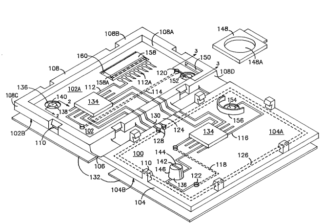
Referring to Fig. 1, a moldable/foldable
housing 100 includes a base member 102, a cover
member 104, and a living hinge 106 joining the base
and cover members. Base member 102 has oppasing
interior and exterior surfaces 102A and B and,
similarly, cover member 104 has opposing interior
and exterior surfaces 104A and B (the interior
surfaces face "up" in Fig. 1 and only the edges of
exterior surfaces 102B and 104B are visible in the
figure). Base member 102 includes a peripheral
wall 108 which extends around the perimeter of the
base. Peripheral wall 108 has interior, upper and
exterior surfaces 108A-C, respectively. The
exterior surface 108D of the peripheral wall
adjacent hinge 106, and thé interior surfaces 108A
are sloped at an angle relative to interior surface
:
4 l 3 1 ~
102A, preferably 70 degrees. These sloping
surfaces 10aA and D facilitate the depositing of
the printed circuit patterns described below.
Housing 100 is illustrated unassembled in
Fig. 1. To complete the assembly, cover 104 is
rotated about hinge 106 until the interior surface
104A of the cover contacts the upper surface 108B
of the peripheral wall. Snap-fit connectors, e.g.
110, are preferably integrally molded with housing
100 and provide a means for fastening cover 104 to
base 102. For certain applications, for example,
when housing 100 is ex~remely thin, it may be
preferable to eliminate the snap-fit connectors and
ultrasonically weld cover 104 to upper surface
108B. Other well known shapes of snap-fit
connectors may also be suitable and other fastening
means, for example, screws, could also be used to
fasten cover 104 to base 102.
Housing 100 is preferably injection molded
from a thermoplastic material, preferably
polyetherimide tPEI). Other thermoplastic
materials may also be suitable, although high
temperature thermoplastic materials are preferred
because the housing is usually exposed to soldering
temperatures. Examples of suitable high
temperature thermoplastic materials include
polysulfone, polyethersulfone, polyamideimide,
polyarylsulfone, polyarylate, polyetheretherketone,
polybutyleneterephthalate, and blended combinations
thereof. It is preferred that all housing parts,
including base 102, cover 104, hinge 106,
peripheral wall 108, snap-fit connectors 110, and
the switch 136 and battery contact 152 described
below, be injection molded from the same mold
(i.e., integrally molded). I~ there are no printed
circuit patterns on cover 104, however, hinge 106
13~6~7~
could be eliminated and the cover manufacturecl separately from the base, The manufacture
of a living hinge is well known in the art of injection molded plastics.
Solderable printed circuit patterns 112 and 114 are respectively disposed
directly on interior 102A and exterior 102B surfaces of the base, and similarly, solderable
printed circuit patterns 116 and 118 are respectively disposed directly on the interior 104A
and exterior 104B surfaces of the cover. Conductive through-holes interconnect opposing
printed circuit patterns. For example, conductive through-hole 120 is electrically connected
between printed circuit patterns 112 and 114, and through-hole 122 is electrically connected
between printed circuit patterns 116 and 118. An interconnecting printed circuit pattern 124
is disposed directly on hinge 106 and is electrically connected between printed circuit
patterns 112 and 116. A printed circuit loop antenna pattern is directly disposed on the
exterior surface 104B of the cover. Conductive through-holes 128 and another
interconnecting printed circuit pattern 130 disposed on hinge 106 provide a means to
connect antenna 126 to printed circuit pattern 112. To protect the external printed circuit
patterns 114 and 116, including antenna pattern 126, thin sheets of mylar or other insulative
material 132 are adhesively bonded over the printed circuit patterns.
All printed circuit patterns are preferably vacuum deposited onto the various
surfaces of housing 100.
,.
.~... ..
-6- 1316~7~
The housing 100 is three dimensional. It is preferred that the printed circuit patterns be
directly disposed (i.e., without any intervening structure between the printed circuit
conductor and the housing, such as a layer of adhesive, or a conventional rigid or flexible
printed circuit board) on the housing surfaces, and other methods of depositing printed
circuit patterns directly onto a molded thermoplastic substrate, such as electroless plating,
are also suitable. E]ectrical components, for example 134, are soldered directly to the
interior printed circuit patterns 112 and 116.
Housing 100 also includes an integrally molded switch, which is illustrated in
cross-section in Figure 2 (in Figure 2, housing 100 is illustrated fully assembled with cover
104 attached to base 102). Referring to Figures 1 and 2, switch 136 includes a thin, flexible
wall 138 onto which a first printed circuit switch contact 140 is directly disposed. The
diameter of flexible wall 138 is approximately 10 millimeters and the thickness of the wall
is approximately 125 microns. Cover 104 includes an integrally molded pillar 142 on its
interior surface onto which two printed circuit switch contacts 144 and 146 are directly
.. ..
7 ~3~7~
disposed. To facilitate the photolithographic
definition of printed circuit switch contacts 144
and 146, pillar 142 is partially conical in shape
with sloping side walls that form an angle of
approximately 70 degrees with khe interior surface
104A of the cover. In operation, pressure is
applied to the exterior surface of flexible wall
138 causing it to deflect towards pillar 142,
whereupon switch contact 140 shorts contact 144 to
contact 146.
A slideable battery compartment 148 includes
an aperture 148A suitable for receiving a thin,
disc shaped battery (the battery is not illustrated
in Fig. 1). Battery compartment 148 slides into
housing 100 through an aperture 150 in peripheral
wall 108, whereupon one of the battery's terminals
contacts battery contact 152 on the interior of
base member 102. Battery contact 152 is connected
to printed circuit pattern 112. In the
alternative, the battery can be mounted internally
(i.e., without the benefit of slideable battery
compartment 148) by retaining the battery within an
arcuate wall 156, which completes slightly more
than 180 degrees of a circle.
In Fig. 3, a detailed cross-sectional view of
battery contact 152 is illustrated. Referring to
this figure, battery contact 152 includes a thin
flexible wall 302 with a protuberance 304 attached
to the thin wall. Thin wall 302 and protuberance
304 are preferably integrally molded with base
member 102. A printed circuit battery contact 306
is directly disposed on the upper surface of
protuberance 304 and is electrically connected to
the printed circuit pattern 112 on the interior
surface of the base. When a battery is installed
in in housing 100 (either directly, or through the
use of a battery compartment 148), printed circult
battery contact 306 is forcibly engaged with the
battery terminal 308A on the battery, causing thin
wall 302 to flex downward and apply pressure on
terminal 308A. A similar battery contact 154 (see
Fig. 1) is located on the interior of cover 104,
but is not illustrated in Fig. 3. Battery contact
154 applies a force to a second battery terminal
308B, equal in magnitude but opposite in direction
to the force exerted on battery terminal 30~A by
battery contact 152. Thin wall 302 and
protuberance 304 are similar in design to wall 138
and pillar 142 of switch 136.
A liquid crystal display (LCD) 158 is
1~ positioned in an aperture 160 in the base.
Electrical contacts, e.g. 158A, on the LCD are
connected to contacts, e.g. 112A, by the use of a
well known heat seal connector, such as those
available from Nipon Graphite Industries. When
housing 100 includes LCD 158, mylar sheet 132
requires a transparent window centered over the
viewing surface of the LCD.
To strengthen base and cover members 102 and
104, an integrally molded structure 402, such as
2~ the one illustrated in Fig. 4, can be used on the
external surface of the member ~this precludes,
however, the use of a printed circuit pattern on
the exterior surface). In the alternative, a
pattern of reinforcing rods 502, such as the one
illustrated in Fig. S, can be integrally molded
into the base and cover members.
Other shapes of moldable/foldable housings, besides
the one illustrated in Fig. 1, are also possible,
and the invention can be practiced with more than
two flexibly interconnected housing members (i.e.,
base 102 and cover 104). For example, hinged sides
. .
~31~
could be substituted for the rigid peripheral wall
108, and flat, printed circuit substrates (also
integrally molded with the housing) could be
flexibly attached to one of the housing members and
folded into the housing cavity (the space between
surfaces 102A and 104A) at final assembly, but
after electronic components have been attached to
these additional hinged substrates.
':..
, ,, " ,~
. ~ ,