Note: Descriptions are shown in the official language in which they were submitted.
-` 13~700~
EL-4306
TITLE
Ground Plane Shield Device For Right Angle Connectors
BACKGROUND OF THE INVEN7rION
Field oî the Invention
The present invention relates to a ground plane shield device ~r
impedance and cross talk control between signal calTying conductors emanating
from an electrical connector, and in particular, to such a shield device adaptedfor retro-fitting to a connector that has been previously mounted to a board.
Description of the Pnor_Art
Controlling the interfering electrical effect than an electrical
signal carried on a given conductor exerts on a signal carried on an adjacent
conductor is especially important in high density connectors. Such control can
be implemented in a variety of ways. For example, the most basic technique in
a high density connector is to connector particular ones of the conductors to a
predetermined ground potential, thereby causing such conductors to act similarlyto ground planes and thereky to isolate the signals carried on adjacent
conductors.
An alternative approach is to provide separate ground plane
structures in the connector. Exemplary of this alternative are the devices
disclosed in United States Patent 4,232,929 (Zobawa) and United States Patent
4,558,917 (Kamono et al). In the latter patent the ground plane structures take
the form of separate, spaced vertical plates disposed between adjacent columns
of conductor tails emanating from a connector housing. United States Patent
3,601,756 ~Stroh~ discloses a connector in which a ground plane structure is
sinuously wrapped about the signal carrying conductors. Copending Canadian
application Senal Number 543,648 filed on August 04 1987 and copendîng
Canadian application Serial Number 551,742 filed on N~vember 12 1987, both
assigned to ~e assignes of ~e present
~, ..
1 31 7004
invention, rclatc to shielding schemes for use in cables and in cable
conrlectors.
It is more difflc-llt to control the impedance and
crosstalk efrects in connectors that have not been previously
dcsigned to contain suitable interference control structures once
such a connector has bcen mounted in position on a circuit board
substrate.
Accordingly, it is believed to be advantageous to provide
a ground plane shield arrangement that is particularly adapted for
10 being expeditiously placed into use with a connector once the same
has already been placed in position on a substrate.
SUMMARY OF THE INVENTION
The present invention relates to a ground plane shield
1~ device for use with a connector mounted to a generally planar
substrate, the connector being of the type ha~ring a housing from
which a plurality of terminal tails emanate. The tails are arranged
in at least one, but typically a plurality of generally parallel columns.
Each of the tails has a flrst portion generally perpendicular to the
2(! housing, a second portion generally perpendicular to the substrate,
and an intermediate portion connecting the flrst and the second
portions .
The ground plane shield device comprises a conducting
member formed to define a first and a second panel arr~nged in
2~ genera~ly confrontational spaced relationship with respect to each
other, the panels defining a space therebetween. Each panel has at
least a ~irst, connector, ed~e and a second, substrate, edge. A ~Irst
and a second clip are disposed on each panel in corresponding
locations along the connector and the substrate edges, respectively.
30 The clip along the connector edge of each of the panels and the
clip along the substrate edge of each of the panels extend toward
the corresponding clip on the other of the panels thereby to place
the corresponding clips into predetermined close proximlty to
each other. Each of the clips has a cutout therein, each cutout
1 3 1 7 0 0 At
l~cillg si~ed to rcceive and to grasp a predetermincd portion of a
prcdetermillcd one of thc tails in the column of tails, such that, in
use, with the cutouts in the clips along the conncctor edges of the
panels grasping the first portion of the prcdetermined one of the
5 tails in the col--mn and with the cutouts in the clips along the
substrate edges of the panels grasping the substrate portlon of the
same predetermined tail the intermediate portion of all of the tails
in the column is received in the space between the panels.
In the preferred instance the member is formed to
10 define the panels by folding along a first fold line and along a
second fo]d line generally parallel to the ~lrst whereby the ground
plane shield device is a generally U-shaped member having a closed
face defined between the fold lines and three open faces defined
between corresponding edges of the panels.
BR~EF DESCRlPTlON OF THE DRAWINGS
The invention will be more fully understood from the
following detailed description thereof, taken in connection with the
accompanying drawings, which form a part of this application and
'~ O in which:
Figure 1 is a rear perspective view of a prior art
connector having an array of right angle conductor tails emanating
therefrom;
Figure 2 is a highly stylized rear perspective view of a
25 ground plane shield device in accordance with the present
invention with portions thereof removed for clarity of illustration,
the shield device being disposed w~th respect to a substrate ~ith
the closed end of the device parallel to the surface of the substrate:
Figure 3 is a front perspective view of a board mounted
30 connector such as shown in Figure 1 with the ground plane shield
device in accordance with the present invention being disposed
w~th respect thereto in an alternate position from that sh~wn in
Figure 2, with one of the ground plane shield devices being
exploded from its position, with securing means for securing the
131700~
sllield dcvice to the board being illustrated as in sccuring position
(so]id lines~ and in retracted position (dotted lines);
Figure 4 is an en]arged view of the exploded portion of
Figure 3 again with a portion of the securing means ~or securing the
shield device to the board being illustrated as in securlng position
(solid lines) and in retracted position (dotted lines); and
Figure 5 is a plan view of a b1ank rrom which the grourld
plane shield device in accordance with the present invention is
form ed .
DF,TAII,ED DESCRlPrlON OF THE lNVENTION
l`hroughout the ~ollowing detai~ed descriptlon, similar
reference numerals will refer to similar elements in all figures of
the drawings.
Figure 1 illustrates a rear perspective view of a typical
connector of the prior art generally indicated by reference
character 10. Exemplary of connectors similar to the connector 10
shown in Figure 1 are the devices manufactured and sold ~r E. 1. Du
Pont de Nemours and Company, Incorporated as the DIN 41612-
'~0 series C connector and the DIN 41612-Series R connector. The
connector 10 is suitably mounted to a substrate 12, such as a
printed circuit or pnnted wire board in a manner to be discussed,
although in Figure 1 it is spaced a predetermined distance
thereabove for clarity of illustratlon.
2~ The connector 10 has a generally rectanguloid housing
16 formed of an insulating material. To effect the mounting of t~e
connector 10 to the board 12 t e housing 16 is provided, in a
typical instance, with a mounting abutment 18 at each end thereof.
Only one of the abutments 18 is shown in Figure 1. The abutment
18 has a planar shelf 20 thereon and a mounting opening 22
therethrough through which a mounting screw or the like may pass
to secure the connector 10 to the board 12. The housing 16
extends a predetermined height dimension H above the surface of
the board 12 when the connector 10 is mounted thereto.
1 31 70~-~
Disposed within the housing 16 is a plurality of
electrical contacts of eithcr the male of female type. Each of the
contacts has a ~ail generally indicated by the rercrence character 26
associ~ted therewith. In Figure 1 the tails 26 emanate from the
5 rear surface 30 of the housing 16 in an array containing a
predetermiIled plurality N of vertical columns 34-1 though 34-N
(Figure 4). Only four such adjacent columns 34-1 through 34-4 are
ShOWIl in Figure 1. Each column 34 contains a vertically aligned
stack of conductor tails 26. Although any predetermined number of
10 tails 26 may be arranged in each stack, in Figure 1 each column 34
is shown to contain three such tails 26, with the top tail in a given
column is indicated by the suffix "r', the middle tail being
indicated by the suffix "M", and the bottom tail being indicated by
the suffix"B".
It is a typical practice in the art that one of the eontacts
associated with one of the tails 26 in each of the colurnns 34 be
connected to a predetermined ground potential. As used herein, it
should be emphasized that ground potential is referenced from the
point of view of a signal carrying conductor. Thus, the terrn is
construed herein to include power connections, chassis grounds,
and logic grounds. The tail 26 itself therefore also lies at this
predeterrnined ground potential. For purposes of discussion herein
it is assumed that the middle tail 26M in each of the columns 34 is
connected to this predetermined ground potential. ~,ach of the
columns 34 has a predetermined transverse dimension 36
associated thcrewith, where the dimension 3Ei includes the
transverse dimension of the tail 26 itself as well as ~ome
predetermined buffer distance adjacent each side of each of the
tails.
Each of the tails 26 compfises a first portion 38, a
second portion 40 and a third portion 42. The ~irst portion 38 is
termed the connector portion since it is in proximit~ to the rear
surface 30 of the housing 16 and lies generally perpendicular
thereto. The third portion 42 is termed the substrate portion since
~ 31 700 ~
it is proximal to and gcnerally perpendicularly arrangcd with
respect to the substrate 12. When the connector 10 is aff~xed to
the substrate 12 the third portion 40 of each of the tails 26 extends
through an opening 14 prov~ded in the substrate 12. The second
portion 40 is intermediate the flrst portion 38 and third portion 42
and, in the prior art connector illustrated, contains a generally
right angle bend therein. Of course, it should be understood that
the portions 38 and 42 need not, as is illustrated, be completely
perpendicular to the connector and the board, nor, ~s illustrated,
must the intermediate portion 40 be a right angle bend, inasmuch
as the present invention may be configured ~or use with alternate
configurations of these elements.
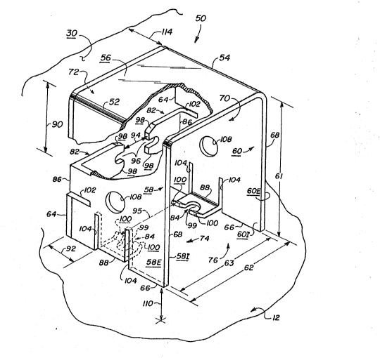
Figure 2 is a highly styli~ed rear perspective illustration
of a ground plane shield device generally indicated by the reference
character 50 in accordance with the present invention, with
portions thereof removed for clarity. The device 50 is adapted to
be retro-~it to a connector 10 already positioned on and secured to
a substrate 12. The device 50, in the preferred case, comprises a
member made of a conducting material, such as phosphor bronze or
berylliurn copper. Preferably the dev~ce 50 is formed, as will be
discussed, by ~olding the same along a first fold line 52 and a
second fo]d line 54 to dehne a generally U-shaped structure having
a web portion 56, a first panel 5~ and a second panel 60.
Each panel 58, 60 is generally square in shape and
preferably has a dimension 61 that is selected such that when the
device 5~ is in posStion about the tai~s (and there supported in a
manner to be described~ the top sur~ace of the web 56 is spaced
above the substrate 12 a distance substantially equal to the height
dimension H of the housing 12. The panels 58, 60 each have an
interior surface 581, 60~ and an exterior surface 58E, 60E thereon.
The exterior sur~ces 58E, 60E of the panels are spaced by a
predetermined distance 62, while the interior surfaces are spaced
a predetermined distanee 63. The distances 61, 62 and 63 can
have any desired relationship with respect to each other, ~t being
13170~
only necessary that the distance 63 be substantially equal to the
distance 36, for reasons that should bccome apparent herein.
It should be understood that the panels 58, 60 may be
formcd by bendil-g or folding a planar member along a slngle,
double (as i?~ustrated) or other predetermined number of multiple
folds or by rolling the same and, in all events, remain within the
contemplation of the present invention. Thus, for example, it
should be understood that the device 50 may be formed with only
one fold line, in which event the devicc has imparted thereto a
generally V-shape. Alternately, more than two fold lines may be
used to define the panels, in which event there is imparting a
generally corrugated configuration to the web portion 56 of the
device 50. Yet further, the member may be formed by rolling in
which case the upper portion thereof will exhibit a generally domed
1 5 shape.
Each panel 58, 60 has a flrst, connector, edge 64, a
second, substrate, edge 66, and a third, free, edge 68 thereon. The
fourth edge of each panel 58, 60 is defined by the respective fold
line 52, 54. l`he panels 58 and 60 lie generally parallel to each
other in confrontational spaced-apart relationship. The panels 58,
60 and the web 56 cooperate to define an interior space 70. The
device 50 has a first open face 72 deflned between the opposed
connector edges 64 of the panels 58, 60, a second open face 74
defined between the opposed substrate 66 edges of the panels 58,
60, and a third open face 76 defined between the free edges 68 of
the panels 58, 60. The fourth ~ace of the device 50 is closed by the
web 56 defined between the fold lines 52, 54. In the embodiment
shown in Figure 2 the web 56 is, in use, disposed generally parallel
to and spaced in overlying relationship with respect to the
substrate 12. However, the device 50 may be used with ~he web 56
disposed perpendicular to the surface of the substrate 12. Thus. as
seen in the embodiment shown in Figures 3 and 4, the edges
defining the connector edges 64 and the substrate edges 66 differ
~rom those shown in Figure 2. In Figures 3 and 4, the connector
1 3 ~ 7 o O !9r
edges 64 are dcrlncd by the edges of the panels opposite from the
fold lines 52, 54 dei~lning the web 56 while the substrate edges 66
are derlned by the edges adjacent to the web 56.
Each panel 58, 60 has a first clip 82 and a second clip
5 84 disposed in corresponding locations along the edges of the
panels defining two of the three open faces. Tn the embodiment
illustrated in Figure 2 the device 50 is shown to have clips 82, 84
on the faces 72, 74 respectively defined by corresponding
connector edges 64 and corresponding substrate edges 66. That is,
10 in the embodiment of Figure 2 the c]ips 82 are provided on the face
72 defined on th~ connector edges 64 Iying adjacent to the web 66
and the clips 84 are defined on the substrate edges 76 that lie
opposite from the web 56. In the embodiment illustrated in
Figures 3 and 4 the device 50 is shown to have the clips 82 on the
15 face 74 defined by corresponding connector edges 66 and the clips
84 on the face 76 defined by corresponding substrate edges 68. It
should be understood that consistent with the foregoing discussion
the device 50 may be configured to have only two open faces (i~e., a
connector face 72 and a substrate face 74) or more than three open
20 faces. if desired. Any of these alternative configurations is to be
construed as Iyir~g within the contemplation of the invention.
Each clip 82 is formed on the respective panel on
which it is disposed by folding the matelial Or the panel along a fold
line 86 toward the confrontationally disposed other of the panels.
25 The clips 84 are formed on their respective panel in a similar
manner by folding the material of the panel along a fold line 88
toward the confrontationally disposed other of the panels. Each of
the fold lines 86, 88 lies generally parallel to the edge of the panel
on which the clip is associated. The clips 82. 84 are spaced a
30 respective predetermined distance 90, 92 along the edge of the
panel from which it is defined for a purpose to be made clearer
herein .
-
~ ~ 1 7 oo i'l~
Whcn formed thc conrronting pairs of clips 82, 84 lie
are spaced apart a predetermined close distances 94, 95. The
magnitudes Or the distances 94, 95 are related to the thickness
dimension of sclectcd predetermined portions of the talls 26. It
5 shou]d be understood that the clips 82, 84 may take a variety of
forms, so long as they are arranged so as to support the shield above
the substrate and from the connector and so as to engage the
predetermined portion of a selected one of the tails and thereby
electlically connect each panel of the shield to the tail at both
10 points where the clips 82, 84 engage the same.
Each clip 82 has a cut-out 96 fonned therein, ~he cut-
outs 96 being bounded on each side thereof by a lead-in surface 98.
Similarly, each of the clips 84 has a cut-out 99 formed therein. The
cut-outs 99 are bounded on each side thereof by a lead-in surface
100. The panels 58, 60 are preferably slotted~ as at 102, 104,
respectively, in the vicinity of the respective clips ~2, 84 to impart
flexibility thereto. Each of the panels 58, 60 is also provided with a
depression or dimple 108, for a purpose to be described.
In use, the shield device 50 is supported by the clips
20 82, 84 a predeterrnined distance 110 above the substrate 12 and a
predetermined distance 114 from the surface 30 of the connector
10 to straddle a predetermined one of the columrls 34 of the tails
26 emanating from the surface 30 thereof. The desired final
mounted position for the shield 50 is to dispose the cut-outs 96 on
'~5 the clips 82 provided on the connector edges of the shield 50 in
engagement against the connector portion 38 of the tail 26M (i.e.,
the tail connected to ground potential) and to dispose the cut-outs
98 on the clips ~34 provided on the substrate edges of the device 50
in engagement against the substrate portion 40 of the tail 26M.
30 When so engaged, the remainder of the tail 26M as well as the
entirety of the remaining tails 26T and 26B in the selected column
34 lie within the space 70 encompassed by the confronting panels
58, 60 and the web 56 of the device 50. As the device 50 straddles
the selected co]umn the dimples 108 on the panels 58, 60 abut
1~70~
agai-lst the intermediate porUon 42 of the tail 26M, thereby
providing mourlting stability to the device 50, The distanccs 90, 92
are, thcrefore, selccted to position the clips 84, 86 so that they are
respec~ively adjacent to the portion of the tail against which they
5 grasp and, simultaneously when so grasping the appropriate portion
of the tai], to support the device 50 the distances 110, 114 from
the subslrate 12 and the face 3t) of the connector 10. As noted
earlier thc top surface of the web 56 should preferably be spaced
aibove the substrate 12 a distance substantially equal to the height
1 0 dimension H of the housing 12.
The panels 58, 60 are introduced over the selected
column 34 in a manner that brings one set of clips and then the
other set of clips over the tails in the column. As the clips 82 and
84 are moved over the tails 26, they are urged apart owing to the
15 reaction of the lead-in 98, 100, as the case may be, against the tails
26. The resiliency imparted to the clips 82, 84 by the slots 102,
104, respectively, in ~he panels ~8, 60 assists in this action. Note
that if the motion of the device 50 is sufficiently fast the clips 82,
84 move past any preceding tail 26 before the clip can resiliently
20 return into gripping position, thus to prevent a clip from clasping
onto other than the tail of interest.
The gripping engagement of the clips 82, 84 and the
tail 26M serves to properly terminate the panels 58, 60 and
electrically interconnect the device 50 to the same potential at
25 which the tail 26M is maintained. For this purpose the dev~ce 50 is
~herefore, preferably fabncated of a conductive material. However,
it should be understood that the member may be other than a
conductor, if the interior surface of the panels thereof and the clips
are lined with a conductive material to establish the electrical
30 connections to be discussed. The panels are sized to provide a
sumciently ]arge surface so that ground return currents associated
with the signal carrying conductors disposed within the space 70
and surrounded by the device 50 can ~low in the panels as needed
to minimize the inductance associated with ~e ground path.
1~
1 1
1 31 700'~
SilIce, ir~ practice, it is the usual case that each co]umn
34 includes a tail 26 that is eonnccted to the predctermined
ground potential it is anticipated that shield devices 50 in
accordance with the invention will thererore, in use, be provided
5 over alternate columns of tails. Figure 3 l\lustrates a typ~eal
instance of this arrangement. It should also be understood that the
particular one of the tails in a column that is connected to ground
potential may vary, possibly from column to column across the
connector. Thus, in such instances the magnitude of the distances
10 90 and 92 will then depend upon the location of the particular one
of the tails so connected to ground potential such that the
interconnection between the grounded tail and the shield can
occur.
However, it also lies within the contemplation of the
15 invention to si~e the interior transverse dimension 63 of the device
50 to a degree that the panels 58, 60 are able to encompass more
than one of the columns of tails. That is, the interior dimension 63
may be substantially equal to or greater than twice the distance 36,
or some other desired multiple thereof. In this even~ the clips 82,
20 84 on one of the panels w~ll contact against one of the ground
potential tails while the clips 82, 84 on the other of the panels will
contact against a different one of the grounded tails.
As an aid in holding the devices 50 in place securing
means 110 for holding the shield dev~ces 50 in their desired
25 disposition over the selected column(s) of tails is provided. In the
preferred instance ~he securing rneans 110 compfises an elongated
comb-like member 112 formed from an insulating plastic material.
The member 1 12 includes a baseplate 1 14 having mounting
abutments 116 at each end thereof. The abutments 116 are initially
30 provided wi~h upper and lower fastening tabs 118A, 118B. Each tab
1 18 has an aperture 1 19A, 1 19B respectively therein. An array of
teeth 120 extends from the baseplate 112.
1 3 1 700~
The irldividual teeth 120 are arrangcd in pairs 122
across the length of the bascplate 114 (as shown in Figure 3),
except near one end thereof, where a single, unpaired tooth 124 is
provided. The gap 128 between the interior confronting surraces of
the teeth 120 in a given pair 122 is substantially equal to the
dimension 36 ~Figure 1) of a column 34 of tails 26. These gaps 128
between the interior confronting surfaces of the teeth in a given
pair 122 of teeth are thus si~ed to accept the tails 26 of those
columns 34 over which no shield device 50 is provided.
The distance 130 between the exterior surfaces of the
teeth 120 in any given pair 122 of teeth is substantially equal to the
exterior transverse distance 62 (Figure 2) of each of the shields 50.
The gap 132 between a first tooth in one pair of teeth
and a second tooth disposed in an adjacent pair of teeth is also
15 substantially equal to the exterior transverse distance ~2 (Figure 2)
of each of the shields 50. Thus these gaps 132 are si~ed to
accommodate the device 50 and engage the exterior surfaces 58E,
60E of the panels 58, 60 of a shield 50. If the transverse exterior
dimension 62 of the shield 50 Is enlarged, as discussed earlier, or if
20 the transverse dimension 62is diminished for electrical reasons,
the above-discussed distances bet~,veen the surfaces on the teeth in
a given pair of teeth and the distances between surfaces on teeth in
adjacent pairs of teeth are commensurately altered.
The gaps 136 and 138 provided between the abutments
116 and the first pair 122 of teeth at one end of the baseplate 114
and between the other abutment 116 and the unpaired tooth 124 at
~he other end of the baseplate 114 are respectively sized to
substantially equal the exterior transverse dimension 62 and
substantially one-half of the exterior transverse dimension 62 of the
30 shield device 50. Thus, the member 112 may accommodate an
arrangement of shield devices 50 in which the first column 34-1 of
the tails 26 is covered by a shield device (in which event the end of
the baseplate 114 having the larger gap 136 is used ad,)acent to that
end of the connector 10) or in whieh the second column 34-2 of
1 3 1 700 -~
the tails is covered by a shield device 50 (in which event the end of
the l~aseplate 114 having the smaller gap 138 is used to surround
the exposed flrst column 34-1 of tails).
As noted the abutments 116 have fastening tabs 118A,
5 118B origillally provided thereon. Depending upon which end of
the baseplate 114 (i.e., the end having the gap 136 or the end
having the gap 138) is positioned adjacent to the end of the
connector housing 16 the appropriate ta'b 1~8A, l18~3 is removed.
Thus the remaining tab 1 lB is po~itioned on the shelf 20 so that
O the aperture 1 19 in the tab 118 registers with the opening 22 in
the abutment 18. With the opening 22 and the aperture 119
aligned any suitable mounting hardware, such as the fastener
schematically indicated at reference character 140 (which form
part of the securing means 110) may pass to hold the member 112
15 and the connector 10 to the board 12. The member 112 may be
used with either the embodiment of the invention shown in Figure
2 (in which the web 56 is parallel to the board 12) or in the
embodiment of the invention shown in Figures 3 and 4 (in which
the web 56 is perpendicularly to the board :l2). In a given
20 application some of the shields may be disposed as in Figure 2 and
others as in Figure 3, if desired.
With reference to the plan view of the blank 142 shown
in Figure 5, the manner in which the shield devices 50 are formed
from the blank may be understood. Each of` the indiv~dual
25 developed shields 50 are connected to a lead frame 144 by a tab
146. In a ~irst manu~acturing operation, the dimple 108 is stamped
into the panels 58, 60. Thereafter, using a progressive die pair, the
ends of the clips 82, 84 are ~olded one hundred thirty five degrees
along fold lines 150, 152 toward the panel with which they are
30 associated. l~he clips 82, 84 on each of the panels are then
themselves folded along the fold lines 8B, 88. ~inally the member
is folded along the ~old lines 52t 54 to define the panels 58, 60and
the web 56. The comb 114 is fbrmed by extrusion from a die and
subseguently sliced.
1~1700'1i
Those skilled in the art, having the benerit of the
teacl~ gs of the prcsent invention as hereinabove set ~orth, may
effect nulllel-ous modirlcations thereto. It should be understood,
however~ that such modil`lcations are to be construed to lie within
5 the contemplation of the present invention, as defined by the
appellded claims.
14