Note: Descriptions are shown in the official language in which they were submitted.
1 3~7~
DIG~: Olo
s
HIERARC~ICAL ARBITRATION SYSTEM
lS This invention relates ~enerally to the field of data
processing, and more particularly to the arbitration of
simultaneous service requests. Specifically, the
invention relates to a computer interconnect coupler which
arbitrates the transmission of addressed data packets
among various data processing devices.
A conventional digital computer system comprises at
least a memory, an input-output device, and a data
processor. The memory stores information in addressable
2S storage locations. This information include~ data and
instructians for processing the data, including commands
and responses. The data processor transfers information
to and from the memory, interprets the incoming
information as either data or instructions, and processes
the data in accordance with the instructions. The input-
output device also communicates with the memory in order
to store input data and output processed data.
A small computer system typically includes a central
processing unit, memory, an input-output unit, and a power
supply maunted together in a cabinet. The cabinet is
` ' ' ~
.... .
~3~3:~
built around a frame having a rack or "card cage" defining
parallel-spaced slots for receiving printed circuit boards
including the central processing unit, memory, and input-
output unit. The interior edge portions of the circuit
boards include terminals which mate with connections on a
"back plane" of the card cage. The "back plane" has a
number of parallel conductors or buses which interconnect
the boards, connect the boards to the power supply, and
connect the input/output unit to a number of input/output
ports. The buses convey addresses and data, control and
status signals, and power and ground. The input/output
ports typically include a port for a console terminal, and
at least one port for a high-speed input-output device or
mass memory such as a floppy disc drive, a tape drive, a
high-speed printer, or a hard disc drive.
.
Advances in circuit technology have made it practical
to use additional data processors dedicated to serving
; respective memory or input/output devices. Therefore, in
; 20 the cabinet for a typical central processing unit, there
is likely to be found a first data processor used for
numerical computations, and a second data processor used
for controlling the central memory, for example, for
formatting or buffering input-output data in one portion
of the memory while numerical computations are being
performed on data in another portion of the memory.
Moreover, the input-output or mass memory devices external
to the cabinet for the central processing unlt typically
have at least one data processing unit or "server" for
buffering data and for controlling the devices in response
to high-level commands from a central processor.
'
In recent years, a need has arisen for computation
and data storage capabilities exceeding those provided by
a few central processing units. For special applications,
such as large-scale simulation, these data processing
- . .. .
. .
_3_ ~ ~ 7~1
needs can onLy be met by large computers having a number
of central processors and memory linked together by
addressr data, and control buses. F~r general
applications, however, it is more economical to construct
computer networks wherein a number of conventional central
processing units, input-output devices, and mass memory
devices are located at different positions and are
interconnected to communicate with each other. Typically
the central processing units share o~e or more mass memory
units to access and update a common data base.
Although there are numerous information transfer
schemes which could be used for communication among the
data processing devices in a network, the typical method
is to use a shared communications resource ~i.e., channel
or bus) which interconnects the various elements. In
general, a transmission between two devices over a shared
bus requires two steps, since each device has the
capability of originating a transmission at the same time.
The first step is for the initiating unit to obtain
control of the bus for some more or less defined interval.
The second step is for the initiating unit to transfer
information over the bus.
Obtaining control of the bus requires arbitration to
select a particular one of the devices desiring bus
access. There are two general approaches to arbitration,
which are known as "central" arbitration and "distributed"
arbitration. In central arbitration, a single, central
priority circuit or device receives all requests for bus
access and determines which requesting device at any given
time should be accorded the greatest priority and allowed
to use the bus~ Once that device is selected, it is
allowed to control the bus and effect the transfer. By
contrastr in distributed arbitration, each unit connected
; to the bus is assigned a specific priority and each unit
.:
_4_ ~ 6~_ 7~j3 ~
individually determines whether it has sufficient priority
to obtain control o~ the bus when it desires to do so. If
a unit of higher priority simultaneously seeks bus access,
a device of lower priority must wait until some later time
when it is the highest priority requester.
A distributed arbitration scheme known as "carrier-
sense multiple access with collision detection" (CSMA/CD)
permits a number of devices to communicate over a single
bit-seri~l line such as a coaxial cable. Each device
includes circuitry for monitoring the channel and
indicating whenever two devices are transmitting at the
same time. When a device which is transmitting detects
that another device is transmitting at the same time, the
two devices stop transmitting. Both then retry
transmission after the channel is clear~
One kind of conventional coaxial cable serial data
communication network is known as "Ethernet.l The
Ethernet operates at up to 10 megabits per second and
typically provides up to 1,023 addressable devices on a
segment of the network. The Ethernet is especially useful
for linking a large number of timesharing terminals to a
central processing unit.
~ igh speed information transfer over a shared bus
between separate data processing devices involves
additional requirements such as rapid synchronizationl
isolation, and highly reliable data transfer. Special
hardware and communications protocols have been devised to
meet these requirements.
Dùe to variations in propagation velocity, it is
relatively impractical to transmit data at high speed in
parallel fashion over a multi-line bus connecting distant
data processing devices. Also, due to the requirement of
~ 3 ~ rD~
fast, synchronization, it is undesirable to transmit data
in a non-return-to-zero format. Preferably one or more
serial data streams are transmitted in a modulated or self-
clocking format. The preferred format is Manchester
encoding, as described in Stewart U.S. Pat. 4,592,072 and
Stewart et al. U.S. Pat. 4,450,572. Manchester encoding
also has the advantage of removiny the DC and lower-
frequency components of the data signal, so that theencoded signal will readily pass through simple isolation
transformers.
Reliable data transmission is especially important in
computer networks having a shared data base. In such a
case, any interruption in the updating of a data base must
be detected by the updating central processor in order to
correct the errors which may occur, and al50 the
interruption must be detected by the memory server in order
to prevent other central processors from using partially
changed or obsolete data.
A communications protocol for achieving reliable high-
speed data transmission is disclosed in Strecker et al.
U.S. Pat. 4,560,985. Arbitration is preferably performed
on a rotating or "round robin" basis so that on the
average, each data processing device on a shared channel
has an equal chance of obtaining access. The absence of a
carrier on ths channel indicates that a data processing
device may attempt to obtain access. An arbitration timer
indicates transmission failure when the carrier fails to be
absent within a certain timeout period. Collisions of data
packets or other transmission errors are detected by an
error detecting code such as a cyclic redundancy check.
When a data processing device correctly receives a
data packet, it immediately acknowledges receipt of that
R
,
.
-6- ~ 3 ~
packet by return transmission of an acknowledgment code.
If the data packet was processed upon receipt, a positive
acknowledgment code (ACK) is returned. If the information
packet was correctly received but could not be processed,
a negative acknowledgment code (NAK) is returned. In a
typical case, the negative acknowledgment code signals
that the received data packet could not be processed upon
receipt due to unavailability of a buffer, and therefore
the received data packet was discarded.
Arbitration for transmission of the acknowledgment
code is not required; the code is transmitted as soon as
the carrier of the received data packet is removed from
the transmission channel. Transmission of the
acknowledgment code must be completed within a certain
time period. After this time period, the other data
processing devices may begin to arbitrate and transmit
additional data packets.
If a data processing device fails to receive an
acknowledgment code immediately after transmission of a
data packet, retransmission should be attempted
consecutively up to a predetermined number of times.
Similarly, if a negative acknowledgment code is received,
retransmission should be attempted for a somewhat greater
number of times. In order to break deadlocks, a
pseudorandum or "coin flip" decision should be made when
the data packet is available for retransmission. If the
result of the decision is TRUE, retransmission is
attempted. If the result of the decision is FALSE, the
data processing device waits for a certain delay time
interval and repeats the decision process. The delay time
interval, for example, should be at least the minimum
amount of time for all of the data processing devices to
access the channel; in other words, if all of the data
processing units were attempting retransmission, there
.
_ 7 _ ~ ~3 ~3~
should be some time available for the transmission of data
packets and retransmission of acknowledgment codes, aside
from the time re~uired to detect collisions and arbitrate.
Alternative transmission channels are required to
assure high availability and reliability in communication.
As disclosed in Strecker et al. U.S. Pat. 4,490,785, the
selection of alternative channels should be made on a
random basis, with all channele being equally probable.
The task of channel selection should be done by an
interface circuit which is shared among the alternative
channels.
For coupling data processing devices which use the
above-mentioned communications techniquas, a cluster of the
devices are typically connected directly to a pair of
centrally located signal transformers having a separate
winding for each device. Each transformer provides a
shared channel interconnecting the data processing devices,
and the central location of the transformers assures a
minimal transmission delay. Such a computer interconnect
coupler, however, has a somewhat limited connectivity due
to the limited transmission bandwidth or throughput of the
shared channel. If additional data processing devices were
to be interconnected to a central transformer, each
processor would be guaranteed a proportionally smaller
share of the transmission bandwidth. Therefore, to
interconnect additional data processing units, it is
necessary to add additional channels so that transmiæsion
may occur simultaneously over a number of channels. In
this case, however, each data processing unit must be
~rovided with additional ports and interface circuitry.
Moreover, the ports and interface circuitry cannot merely
be duplicated since additional means arP required for
seleating a particular port for transmission, and obtaining
incoming data from a
: ~
-8~ 7~
particular one of the ports. It is especially undesirable
to make such modifications on existing computer equipment.
The primary goal of the present invention is to
provide an improved computer interconnect coupler which
provides increased connectivity and bandwidth but does not
require substantial modifications to existing computer
equipment.
Another objective of the invention is to provide such
an improved computer interconnect coupler with the
capability of easily changing the configuration of the
cluster of interconnected devices. A related objective of
the invention is to provide such a coupler with redundant
channels and insure that the configuration is consistent
for each redundant channel.
Yet another objective of the invention is to provide
such an improved computer interconnect coupler with the
capability of incremental expansion to interconnect
additional computer equipment.
To attain these and other objectives, a computer
~ interconnect coupler is provided which has a plurality of
; 25 ~alternative junctors for interconnecting respective
channels of numerous data processing devices. The
computer interconnect coupler has logic circuitry for
routing addressed data packets by selecting an available
junctor. In order to minimize the complexity of the
; 30 routing circuitry, it i5 preferable to share the routing
circuitry among the source and destination channels. It
is possible, however, that more than one source channel
may re~uest service at the same time. To minimize the
required processing capability of the routing circuitry,
it is preferable to service simultaneous routing requests
on a time-shared basis and use arbitration circuitry to
-9~
determine the sequence in which the routing requests
are serviced. Under heavy message loading conditions,
this sequence may affect the extent to which each
channel may share the limited capacity of all of the
junctors. A hierarchical rotating priority scheme is
provided to ensure fair arbitration among all
implemented channel circuitry.
: To insure that the limited processing capability
of the routing circuitry is most effectively used, the
different requests to route a message, to queue a
message, and to free a junctor at the completion of a
: 15 message, are grouped and ranked in priority.
Respective duplicate arbitration logic is provided for
arbitrating the requests in each priority grGup.
The present invention may be summarized according
to a first broad aspect as a computer interconnect
coupler for transmitting messages among multiple data
processing devices each of wh:ich has a communication
port, said coupler comprisingo a plurality of
electronic switching means each of which is connected
to a communication port of one of said data processing
~evices to provide a communication channel for
receiving messages from and sending messages to that
device, said switahing means having separate r~ceiving
means and transmitting means for each of said channels,
a plurality of connections associated with each of said
switching means for transmitting messages among said
switching means, central switch logic means connected
to all of said switching means for assigning
; connections to transmit the messages arriving at one of
said switching means from a source device to a
switching means connected to a destination device
designated by ~he message, and hierarchical rotating
arbitration means for arbitrating the assignment of
-9a~ ~ 3 ~ 7 ~ ~ ~
connections for messages transmitted simultaneously by
different data processing devices, said arbitration
means including ring channel~group arbitration means
for selecting different preselected groups of channels
to which connections are to be assigned for the
transmission of message, and ring channel arbitration
means for selecting different channels in a selected
group to which connections are to be assigned for the
transmission of messages.
According to another aspect, the invention
provides a method of transmitting messages among
multiple data processing devices each of which has a
communication port, said method comprising the steps
of: transmitting messages over a respective
communication channel from the port of each data
processing device to a respective electronic switching
means having respective receiving means and
transmitting means for that particular device, each of
said messages including address data identifying the
desired destination of the message, selecting a
connection for transmitting each message arriving at a
receiving means to the transmitting means of the
electronic switching means for the data processing
device at the destination identified in the message,
: connecting the selected connection to the switching
means of the message-originating device and the
destination device, transmitting each message from the
switching means of the message-originating device via
the selected connection to the transmitting means for
the destination device, and then on to the destination
device, arbitrating the selection of connections for
messages transmitted simultaneously by different data
processing devices by sequentially selecting different
'.
-9b- 13~ 1~3 ~
preselected groups of devices to which connections are
to be assigned for the transmission of messages, and
sequentially selecting different devices in a selected
group to which connections are to be assigned for the
transmission of messages.
According to yet another aspect, the present
invention provides a hierarchical rotating arbitration
system for arbitrating requests for services presented
by devices at various times, said devices being
arranged in preassigned groups, said arbitration system
comprising: first rotating arbitration means for
selecting active ones of said groups o~ said devices
presenting requests to be serviced, wherein said groups
of devices have preassigned respective positions in a
first rotational sequence among said groups of devices,
and said first rotating arbitration means selects the
next active group of devices in said first rotational
sequence following the last group of devices previously
having been selected, and second rotating arbitration
means for selecting in the groups selected by said
first arbitration means, devices whose requests are to
be serviced, wherein said devices have preassigned
respective positions in a second rotational sequence,
and said second rotating arbitration means selects the
next requesting device in each selected group in the
second rotational se~uence following the last device
previously having been selected in said each selected
group.
According to still another aspect~ the invention
provides a hierarchical rotating arbitration method for
arbitrating requests for the assignment of transmission
paths for messages generated by multiple data
processing devicesO said devices being arranged in
-
- ~1 3~ 7Q~
preassigned groups, said arbitration method comprising
the steps of: selecting active ones of said groups of
devices for which requests are to be serviced for the
transmission of messages, wherein said groups of
devices have preassigned respective positions in a
first rotational sequence among said groups of devices,
and the different preselected groups of devices are
selected by selecting the next active group of devices
in said first rotational sequence following the last
group of devices previously having been selected, and
selecting in said selected groups, different devices
presenting requests to be serviced for the transmission
of messages, wherein said d2vices have preassigned
respective positions in a second rotational sequence,
and said different devices are selected by selecting
the next requesting device in each selected group in
: 20 the second rotational sequence ~ollowing the last
device previously having been selected in said each
selected group.
According to a further aspect, the present
invention provides a priority ring arbitrator receiving
respective request signals from a predetermined number
of sources and granting priority to a particular one of
the sources having active request signals, said sources
being preassigned to relative positions in a rotational
sequence, priority being granted to the next source in
said r~tational sequence which presents an active
request, sa.id arbitrator comprising, in combination: a
register for storing data identifying the particular
one of said sources being granted priority, said
register having a set of outputs for transmitting said
stored data, a set of inputs for receiving data
identifying the next source in said rotational sequence
which presents an active request, and a clock signal
9d- ~ 3~ J~
de~ining respective instants in time when the data on
said inputs become stored and asserted on said outputs,
and channel selection logic means including
combinational logic for receiving said data on said
outputs and said respective request signals and
generating said data identifying the next source in
said rotational sequPnce which presents an active
request.
Other objects and advantages of the invention will
become apparent upon reading the following detailed
description and upon reference to the drawings in
which:
FIG. 1 is a pictorial diagram illustrating the use
of a preferred embodiment of the present invention for
inte.connecting numerous conventional data processing
devices;
FIG. 2 is a schematic diagram illustrating how
messages are routed over a junctor from a source
channel to a destination channel, and further showing
how internal messages are routed over junctors for
diagnostic purposes;
FIG. 3 is a schematic diagram showing the
: 30 preferred way in which the circuits o~ the exemplary
embodiment are arranged on circuit boards and how the
circuit boards are interconnected by shared buses;
~' ~. ,~,.
-10~
FIG. 4 is a functional block diagram illustrating the
contrcl paths which are used for routing a message from a
source channel to a destination channel, and further
showing the linkages between a diagnostic processor and
the circuitry which routes the messages;
FIG. 5 is a timing diagram showing the successful
routing of a message from a port of origin to a port o~
destination and the return of an acknowledgment code from
the port of destination;
FIG. 6 is a functional block diagram showing in
greater detail the control circuits, control signals,
memory which stores the present logic state and
lS configuration of the interconnect coupler, and various
timers which s~nse abnormal operating conditions;
FIG. 7 is a schematic diagram illustrating a
hierarchical rotating priority arbitration scheme in which
the service requests have the same level of priority;
FIG. 8 is a schematic diagram showing logic circuits
for implementing a dual level priority scheme in which
service requests are grouped into a set of high priority
requests and low priority requests, and in which separate
arbitration circuits are provided for arbitrating
simultaneous requests occurring within each group;
FIG. 9 is a schematic diagram of a priority ring
encoder;
: FIG. 10 is a Venn diagram:showing how a virtual star
coupler i5 defined as a set of source channels associated
with a set of destination channels;
.
.~. . . .
- . .
~ 3~ i J~.
FIG. 11 shows the memory and logic circuits which
store definitions for up to eight virtual star couplers
and which generate a signal for enabling the routing of a
message frorn a specified source channel to a specified
destination channel;
FIG. 12 is an example of a specific format for a
message transmitted through the computer interconnect
coupler;
FIG. 13 is a schematic diagram of a Manchester
decoder and serial-to-parallel converter with carrier
detection logic;
FIG. 14 is a schematic diagram of a message
synchronizer and a cycle counter for receiver control
logic;
FIG. 15 is a schematic diagram of receiver control
logic for generating a request to route a message;
FIG. 16 is a schematic diagram of receiver and
transmitter logic for message queuing;
;~ 25 FIG. 17 is a schematic diagram of logic circuitry for
a first-in-first-out buffer and for interfacing to a
switch matrix;
FIG. 18 is~a schematic diagram of logic circuitry for
a switch matrix and for receiving signals which indicate
to the transmitters and receivers whether a junctor is
assigned and the identification number of the assigned
~unctor;
'
.
-12- 1~.7~
FIG. 19 is a schematic diagram of the preferred
switching circuitry for connecting the receivers with the
junctors;
FIG. 20 is a schematic diagram of the preferred
circuitry for connecting the junctors to the transmitters;
FIG. 21 is a schematic diagram oE receiver logic for
generating service requests for reversing and dropping a
junctor;
FIG. 22 is a schematic diagram of receiver logic for
detecting changes in the assignment of a junctor to the
receiver;
FIG. 23 is a schematic diagram of transmitter control
logic;
FIG. 24 is a schematic diagram of the central switch
logic which processes service requests for routing
messages, reversing and dropping junctors, and for queuing
and dropping message routing requests;
: FIG. 25 is a schematic diagram of a request priority
decoder used in the central switch logic;
FIG. 26 is a schematic diagram of central switch
logic for determining whether a routing request is
; permissible;
FIG. 27 is a schematic diagram of combinational logic
: which is used by the central switch logic for servicing
requests for reversing and dropping junctors;
.
.
.
.
', , '.... ' ~. , ' ' ' ,: , ' ' ~
- . . :
. .; . ~
,
.
-13- ~ r~
~ IG. 28 is a schematic diagram of combinational logic
used by the central switch logic for queuing a message
routing request;
FIG. 29 is a schematic diagram of combinational logic
used by the central switch logic for routing a message;
and
FIG. 30 is a schematic diagram of combinational logic
used by the central switch logic for dropping message
routing requests.
While the invention is susceptible to various
modifications and alternative forms, a specific embodiment
thereof has been shown by way of example in the drawings
and will herein be described in detail. It should be
understood, however, that it is not intended to limit the
invention to the particular form disclosed, but on the
contrary, the intention is to cover all modifications,
equivalents, and alternatives falling within the spirit
and scope of the invention as defined by the appended
claims.
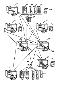
Turning now to FIG. 1, there is shown a pictorial
diagram illustrating the use of a computer interconnect
coupler generally designated 50 which incorporates various
aspects of the present invention. To provide enhanced
reliability, the coupler 50 is comprised of two identical
couplers 51 and 52 which are linked together, for example,
by a fiber-optic link 53~ The link 53 ensures that the
configuration of the couplers 51 and 52 are maintained in
identical states when the state is changed via an operator
request received by either of the couplers 51, 52~ The
couplers 51, 52 may also use the link 53 to share
information about the status and possible malfunctions of
the numerous data processing devices which are
:~ 3 ~
-14-
interconnected by the couplers 51, 52. These data
processing devices include central processing units 54,
55, 56, 57, 58 and servers 59, 60 for magnetic tape drives
61, 62, 63, and mass data storage or disk memories 64, 65,
66, 67, 68, 69. In the usual case, the central processing
units 54-58 are linked directly to high-speed printers 70,
71 or low-speed printers 72, 73 and numerous timesharing
terminals ~not shown), communications devices (not shown),
and application-specific devices (not shown).
The computer interconnect couplers 51, 52 permit the
data processing devices 54-60 to be located at different
positions, for example, at opposite ends of a building.
Moreover, the couplers 51 and 52 may permit any one of the
data processing units in the system to send an addressed
data packet to any other data processing unit in the
system. Further, the couplers 51, 52 can be configured or
programmed to enable message-transmission from one data
processing device to another only if the respective
channels of the source data processing devi~e and the
destination data processing device are included
respectively in the predefined source channel set and
destination channel set associated with at least one
"virtual star coupIer" defined for the system. The
computer interconnect couplers 51, 52 thereby may restrict
access to certain of the data processing devices, may
permit data transfer only in certain directions, and for
security purposes may permit messages to be routed to
certain of the data processing devices only if the
messages first pass through other of the data processing
devices.
In accordance with the specific embodiment shown in
the ollowing drawing figures, eacn of the couplers 51, 52
is a two-stage electronic crossbar switch which preferably
provides eight independent interconnecting communication
:
15~
junctors. Preferably each junctor is bidirectional and
conveys data at 70 megabits per second. Each coupler 51,
52 is preferably capable of interconnecting at least 64
channels. Preferably, the channels connected to the
couplers 51, 52 can be logically divided into as many as
eight virtual star couplers, and the data processing
devices connected to the channels can be moved logically
from one virtual star coupler to another without physical
recabling.
Turning now to FIG. 2, there is shown a schematic
diagram which illustrates the routing of a message frorn a
source channel X to a destination channel Y. The channel
X is defined by a communication cable 81 interconnecting
interface circuits 82 to a data processing device at a
remote location. Similarly, the channel Y has interface
circuits 83 which are interconnected to another remote
data processing device via a second communication cable
85.
For the sake of illustration, it is presumed that the
interface circuits 82 for channel X receive via the
communication cable 81 a message including a data packet
addressed to channel Y. Therefore, for the purposes of
this message, channel X is a source channel and channel Y
is a destination channel. For processing such messages,
each channel is assigned a unique channel number.
For routing the message, the beginning portion of the
message i~ passed from the interface circuits 82 to
receiver logic circuits 84. The receiver logic circuits
84 generate a routing request which, if satisfied, causes
the assignment of one of a plurality of junctors 86 to the
receiver logic circuits 84. The assignment causes a
respective switch in a switch matrix 87 to close and
connect the receiver logic circuits 84 to the assigned
-16- L 3 ~ 7 ~
junctor. As shown in FIG. 2, for example, the receiver
logic circuits 84 are connected to a junctor 88 by the
closure of a switch 89.
The routing of a message to its addressed destination
channel further requires the assigned junctor 88 to be
connected to transmitter logic 92 associated with the
destination channel. For this purpose the transmitter
logic circuits 92 are connected to the junctors 86 by a
switch matrix 90 including a switch 91 which becomes
closed to connect the junctor 88 to the transmitter logic
circuits 92. The required states of the switches in the
switch matrices 87, 90 are set by control signals sent
over a junctor control bus 93. Control signals are also
received by the transmitter logic circuits 92 to indicate
that a link has been established and that a message is
being transmitted over one of the junctors 86. Upon
receipt of the message, the transmitter logic 92 forwards
the message to the channel interface circuits 83 for
transmission over the communication cable 85 ta the
addressed data processing device.
Upon receipt of the message, the addressed data
processing device returns an acknowledgment to the source
data processing device. This acknowledgment is returned
over thP communication cable 85, passes through the
interface circuits 83, and reaches associated receiver
logic circuits 94. In anticipation of receiving the
return acknowledgment when the receiver logic circuits 84
finish transmitting the original message, they cause a
control signal to be generated over the junctox control
bus 93 which opens the switches ag and 91 and closes
switches 95 and 96 to establish a reverse connection
between the receiver logic circuits 94 associated with
channel y and the transmitter logic circuits 97 associated
with channel X. The return acknowledgment is passed by
~, ~ ... .
-17- ~ ~3~
the transmitter logic circuits 97 to the interface
circuits 82 associated with channel X for return to the
data processing unit which initially sent the message.
In order to test the circuits in the interconnect
coupler 51, the interconnect coupler ~urther includes
control and diagnostic logic 98 which is capable of
originating control signals which are passed over the
junctor control bus 93 to establish a "maintenance loop"
through the receiver and transmitter logic of a selected
one of the channels. The control and diagnostic logic 98
generates a diagnostic message which is applied to one of
the junctors 86 via a diagnostic switch matrix 99. For
this purpose, for example, the switches 89, 91 and 95 are
opened and the swit!~h 96 is closed. Moreover, a switch
100 is closed to connect the control and diagnostic logic
98 to the junctor 88 and thereby establish a transmission
path to the transmitter logic 97. The control and
diagnostic logic 98 originates a control signal over the
junctor control bus 93 for closing a switch 101 and a
switch 102 to establish a return path from the receiver
lo~ic circuits 84 to the diagnostic logic 98. In
addition, a complete internal circuit is closed by a
maintenance loop 103 providing a signal path from the
transmitter logic 97 to the receiver logic B4. The
transmitter logic 97 and the receiver loyic 84, for
example, are: disconnected from the interface circuits 82
and inter~onnected via the maintenance loop 103 whenever
both the receiv:er logic 84 and the transmitter logic 97
are connected to the junctors 86 via the switch matrix 87
By comparing the transmitted diagnostic message with the
received diagnostic message, the control and diagnostic
logic 98 can~detect errors in controlling the switch
matrix 87 or improper operation of the switch matrix 87,
the receiver logic 84 or the transmitter logic 97. Any
- 18 - ~ 3 ~
such errors are reported to a system operator 104 via a
control terminal 105~
Turning now to FIG. 3, there is shown a diagram of
various circuit boards which make up one of the
interconnect couplers 51 or 52 of FIG. l. The circuit
boards are mounted in a conventional card cage of the kind
used for a central processing unit, and the circuit boards
are energized by a conventional power supply 111. In the
exemplary embodiment, for example, the power supply, card
cagel and an air blower axe similar to those that are usPd
for a Digital Equipment Corporation "VAX 8600/8650l'
(Trademark) central processor. The "back plane'l of the
card cage, however, is modified to interlink the circuit
boards by a number of buses as shown in FIG. 3.
The exemplary computer interconnect switch generally
designated 51 includes at least a circuit board 112 for a
console and diagnostic processor which provides the control
and diagnostic logic g8 shown in FIG. 2. The diagnostic
processor 112 is, for example, a Digital Equipment
Corporation 'IPDP-ll'' (Trademark) based processor.
Associated with the diagnostic processor are a pair of
floppy disc drives 113, the fiber--optic link 53, and links
to the control terminal, an optional remote device, and a
control panel. The diagnostic processor 112 also has
associated with it a memory board 114 which includes a
program mamory 115 and a data memory 116 for the diagnostic
processor. A pro~ram bus 117 links the diagnostic
processor to the program msmory 115, and a processor data
bus 118 links the diagnostic processor with the data memory
116.
In accordance with a feature of the present invention,
the memory board 114 further includes switch control memory
113 which stores switch routing policy
-19- ~ 3 ~ Pl ~
level information. This information includes, for
exam;ale, a master copy of the definitions of virtual star
couplers for the system, and may also include data
defining the timing intervals for various timers which
detect unusual or improper operating conditions for the
logic circuits in the computer interconnect coupler. A
diagnostic control bus 120 is provided for linking the
switch control memory 119 with the diagnostic processor
112. The diagnostic control bus 120 is also used for
permitting the diagnostic processor to download the policy
level information to central switch logic which routes
messages over selected junctors by controlling the switch
matrices. The central switch logic is included on a
switch control board 121 which also includes the
diagnostic switch matrix (99 in FIG. 2). For downloading
the policy level information and for setting up the
diagnostic switch matrix, the diagnostic processor 112 can
interrupt or send control commands to the central switch
logic in order to address the memory and registers of the
central switch logic, as will be further described below.
The diagnostic control bus 120 is also used to link
the diagnostic processor 112 with electrically erasable
and programmable memory (EEPROM) included on the switch
control board 121 and channel interface boards 1~2, 123
for the purpose of writing diagnostic information to a
faulty circuit board before the faulty circuit board is
removed for repair. Therefore, the diagnostic
information, such as the system state and configuration at
the time the failure was detected and the error flags
which lea to the diagnosis, are carried with the defective
circuit board to the repair facility. This ensures that a
more complete repair will be made to the circuit board so
that, when returned, there will be a greater likelihood
that all of the faults on the circuit board will have been
properly repaired. Along with the diagnostic information,
-20- ~ 3~7$~
the EEPROM for each board preferably includes board
identification information, for example, the type or
function performed by the circuit board, the board's
serial number, the board's manufacturing date and
location, and the repair history of the board.
To provide incremental expansion of the computer
interconnect coupler 51 to accommodate any desired number
of channels up to a certain maximum number, there is
provided a channel interface board 122 for each of a
certain number of data processing devices to be
interconnected into the computer system. Preferably each
channel interface board includes the interface circuits
for eight channels along with the associated receiver
logic, transmitter logic, and switch matrix circuits. The
diagnostic switch matrix in the switch control board 121
is linked to the switch matrices in the channel interface
board 122 via the junctors 86 which extend to the switch
matrices in any other channel interface boards 123 which
may be installed in the system. In order to set and reset
the switches in the switch matrices, the switch control
board 121 is linked to the channel interface boards 122,
lZ3 via the junctor control bus 93.
In order for the channel interface boards 122, 123 to
send routing or queuing requests to the central logic in
the switch control board 121, they are linked via a switch
control bus 124. The switch control bus 124 is also used
for returning acknowledgment signals and sending flow
control signals from the switch control board 121 to the
channel interface boards 122, 123. Moreover, the channel
interface boards 122, 123 are linked to the diaynostic
control bus 120 to permit the diagnostic processor 112 to
download information such as timer intervals to ~he
receiver and transmitter logic, and also to permit the
diagnostic processor to inquire as to the status of the
... .. .
-
-21- ~ 3 ~
counters and registers and the transmitter and receiver
logic.
During the operation of the computer interconnect
coupler, various warning or error conditions may be
generated by the circuitry in the switch control board 121
and the channel interface boards 122, 123. To permit
these conditions of interest to be quickly recognized by
the diagnostic processor, the diagnostic control bus 120
includes a respective interrupt request line far the
s~7itch control board 121 and each of the channel interface
boards. When the diagnostic processor 112 is interrupted,
it addresses an error flag register on the board
generating the interrupt request.
In order to facilitate the operation of the computer
interconnect coupler as the circuit boards 121, 122, 123
are installed or removed, there is provided a separate
status and clear bus 125 which enables the diagnostic
processor to poll each of the slots in the card cage ~not
shown) to obtain information indicating whether a board is
installed, and if so, the type of board and the channel
numbers associated with the board. The status and clear
bus, for example, includes a separate enable line and a
separate clear line from the diagnostic processor 112 to
each of the slots for the circuit boards. The enable
lines are sequentially a~tivated to enable the boards to
transmit a status code along the status bus from a
respective status register. The clear line permits the
diagnostic processor to independently reset each of the
circuit boards 121, 122, 123.
The computer interconnect coupler may further include
a traffic data collection board 126 linked to the
diagnostic processor 112 via a traffic data control bus
127. The traffic data collection board includes, for
,
.
: .
.
-22- ~c~
example, addressable counters which record the frequency
of messages passed over each of the junctors and
originating from or destined for each of the channels.
Turning now to FIG. 4, there i5 shown a functional
block diagram of the computer interconnect coupler
including the important control paths between the various
circuit functions. The channel inter~ace circuits 82
include a line receiver 132 and a line driver 133, which
are coupled to the communication cable 81. The
communications cable 81, for example, consists of a pair
of coaxial cables connected respectively to the line
receiver 132 and the line driver 133 via isolation
transformers (not shown), or alternatively the
communication cable could consist of a pair of fiber optic
lines coupled to the line receiver 132 and line driver
133. In a similar fashion, the other channel interface
circuits 83 include a line receiver 136 and line driver
137 coupled to the communication cable 85. The line
receiver 132 and line driver 133 are connected to their
respective receiver and transmitter logic circuits 84, 97
via a multiplexer 139 which can be switched to provide the
maintenance loop 103. The other channel interface
circuits 83 include a similar multiplexer 140.
The data transmitted and received on the
communication cables 81, 85 are preferably transmitted as
a serial bit stream using a self-modulated or self-
clocking format such as Manchester encoding. The data
rate, for example, is 78 megabits per second. The clock
in the serial bit stream is recovered and the data bits
are framed into eight-bit bytes by a Manchester decoder
and serial-to-parallel converter 141. For ease of circuit
design, a common internal clock is used to process the
data from all of the channels. ~herefore, a synchronizer
142 is used to selectively delay the data byte stream so
,
. '~
.
-23- ~ 4, '~
as to synchronize the data bytes to the internal clock.
The synchronized bytes are fed into a first-in-first out
buffer 143 to provide temporary storage during the routing
of the message. The receiver control logic 84 obtains the
destination address from the header of the message. The
receiver control logic 84 also determines whether the
header conforms to a predetermined format, and if so the
receiver contxol logic sends a service request to the
central switch logic 144 to route ~he message.
To permit the routing of messages only in accordance
with predefined virtual star couplers, the central switch
logic 144 in effect compares the destination address with
a set of predetermined valid destination addresses defined
for the source channel and stored in a central logic
status memory. If the message is addressed to an
impermissible address, the central switch logic 144
rejects the service request for routing the message.
Otherwise, the central switch logic determines whether'a
junctor is free, and also determines whether the
transmitter or receiver at the destination channel is
busy. If a junctor i5 available and the destination is
not busy, then the message is routed. Otherwise, a
message routing request is placed in a "destination queue"
so that the request may be satisfied when the destination
channel is no longer busy.
When a message request is queued, the message in the
buffer 143 cannot be transmitted and is discarded.
Although it could be possible to provide sufficient
storage to store an entire message until the message could
be transmitted, this is not necessary and would réquire an
excessive amount of memory and additional logic
complexity. Moreover, the storase of an entire message
for transmission at a later time reduces the integrity of
the message transmission process since reception by the
-2~ 3~
destination data processing device cannot be immediately
acknowledged. In contrast, according to the preferred
embodiment of the invention, only the beginninq of a
message is temporarily stored and therefore the
acknowledgement of message reception is only slightly
delayed and the computer interconnect coupler appears
relatively transparent to the data processing devices.
In order to prevent the data processing device
connected to the source channel from retransmitting the
message when the message request is queued because the
destination channel is busy, a responsive flow control
signal is sent to the source channel to indicate to the
receiver control logic 84 that the message has been
queued. This flow control signal also activates the
transmitter associated with the source channel to send a
flow control signal back to the originating data
processing device. Upon receipt, the flow control signal
inhibits the data processing device from retransmitting
until the central switch logic determines that the channel
at the destination address is not conveying a message, and
the queued message request appears at the head of the
destination queue. When these conditions are satisfied,
the central switch logic 144 turns the ~low control signal
off so that the data processing device of the source
channel retransmits the message.
If the message routing request is queued because no
junctor is available, no flow control signal is sent and
the data processing device of the source channel is free
to retransmitt the message as soon as it is able to do so~
When the central switch logic 144 is able to route the
message, it sends a signal on the junctor control bus 93
to assign a free junctor to the source channel receiver
and the destination channel transmitter. When the junctor
is assigned, the respective switches in the switch
-25- ~ 3~3~
matrices 87, 90 become closed, and the receiver control
logic 84 and the transmitter control logic 92 are
signalled that a message should be transmitted and
received on the assigned junctor. Prior to transmission,
the receiver control logic 84 adds a tag to the beginning
of the message, and after the tag is transmitted over the
assigned junctor, the message is clocked out of the buffer
143. The tag includes information identifying the
assigned junctor, the source channel numbe~ and the
destination channel number. The transmitter control logic
92 inspects the tag and prevents transmission of the
message if the tag is incorrect. Otherwise, the tag is
stripped off, and a bit synchronization header is added to
the very beginning of the message. The message is then
transmitted through a flow control and data multiplexer
146 and a parallel-to-serial converter and Manchester
encoder 147 for transmission in serial form to the
destination data processing device.
At the end of transmission of the message, the
receiver control logic 84 senses that the buffer 143 is
empty and sends a request to the central switch logic 144
to change the state of the switches in the switch matrices
87, 90 so as to reverse the data flow over the assigned
junctor. Thenr an acknowledgment from the destination
data processing device is returned over the assigned
junctor and transmitted to the source data processing
device. After transmission of the acknowledgment, the
assigned junctor is dropped.
Routing of a diagnostic message occurs in a similar
fashion, except that the consolé and diagnostic processor
112 sends and rece1ves the diagnostic message via a buffer
148 coupled to diagnostic message control logic 149 which
includes transmit and receive logic.
-26- ~3~7~ q
Turning now to FIG. 5, there is shown a timing
diagram of the primary control signals which occur when a
message is received and routed and a corresponding
acknowledgment is returned. The computer interconnect
coupler is set to an initial state by a RESET signal.
After the RESET signal becomes inactive, the receiver of
the source channel X searches for an incoming carrier from
the communlcation cable 81. Upon finding a carrier, the
receiver searches for a character sync code signalling the
start of a message which is indicated by an INTERNAL
MESSAGE signal. After the channel X receiver processes
the initial portion of the message, it sends a ROUTE
MESSAGE signal to the central switch logic. The central
control logic responds by assigning a junctor to the
channel X receiver as indicated by a JUNCTOR ASSIGNED
signal.
From the time that the character sync code is
received, the message is clocked into the buffer 143. As
soon as the junctor is assigned, a prefixing tag is
transmitted along the junctor and then the message is
clocked out of the buffer 143. Transmission of the
message through the junctor continues even after the
entire message has been received by the channel X
receiver, as indicated by the INCOMING MESS~GE COMPLETE
signal. When the buffer 143 becomes empty, signalling
that the entire message has been transmitted over the
junctor, the channel X receiver sends a REVERSE PATH
request to~the central switch logic. Once the path along
the junctor has been reversed, the channel X receiver has
; completed processing of the message.
As a result of reversing the path along the junctor,
the junctor becomes assigned to the channel X transmitter,
as indicated by the JUNCTOR ASSIGNED TO TX OF SOURCE
signal. When the junctor is assigned to the channel X
-27- 1 3 ~ 7 ~ 3 L
transmitter, the transmitter is activated, and the
channel X receiver is inhibited from receiving further
messages. In a similar fashion, during transmission of
the message over the junctor from the channel X receiver
to the channel Y transmitter, the channel Y transmitter is
activated when the junctor is assigned to the channel Y
transmitter.
The initial portion of the message transmitted over
the junctor includes a header byte which includes a code
indicating the type of the message. Upon receipt from the
junctor, if the message is not a positive (ACK) or a
negative (NAK) acknowledgment, the Y channel receiver and
transmitter circuits are placed in an ACK/NAK mode which
indicates that after transmission of the signal, the
channel Y receiver should expect an acknowledgment from
the destination data processing device. In particular, it
indicates to the channel Y eceiver that for a certain
time after the initial transmission of the message from
Z0 the channel Y transmitter, the channel Y receiver is to
expect an acknowledgment, and upon receipt of that
acknowledgment the channel Y receiver need not request
routing of the message because the previously assigned
junctor will have been reserved for return transmission of
the acknowledgment. The ACK/NAK mode also indicates to
the Y channeI receiver that upon completion of message
processing, it is to send a DROP JUNCTOR request to the
central logic instead of a ~EVERSE JUNCTOR request.
:
As shown in FIG. 5, the acknowledgment is indicated
by the RX QF DESTINATIQN INTERNAL MESSAGE signal of the
channel Y receiver. The return message occurs sometime
after the junctor is assigned to the channel Y receiver~
Routing of the return acknowledgment is not required, and
very shortly after the end of the message the channel Y
receiver sends a DROP JUNCTOR request to the central
-. . :~ .
-28- ~ 3 ~
switch logic. Once the processing of the message and the
acknowledgment is finished, the junctor is dropped and the
receiver circuits are returned to their initial state for
receipt of further messages.
Turning now to FIG. 6, there is shown a functional
block diagram of the control logic, control signals,
control memory associated with the control logic, and
various timers which insure that the control signals occur
within certain predetermined time intervals.
For receiving a message, the synchronizer 142 sends a
NEW MESSAGE REQUEST signal to the Manchester decoder and
serial-to-parallel converter 141. The decoder and
converter 141 respond by returning a RX MESSAGE signal
which indicates that a message is being received. At
certain other times, the synchronizer 142 sends a RX CLEAR
MESSAGE signal to the decoder in order to inhibit the
reception of a message. The RX MESSAGE signal is
synchronized to an internal cLock to send an INTERNAL
MESSAGE signal to the receiver c:ontrol logic 84. The
receiver control logic 84 returns an END MESSAGE
P~OCESSING signal after processing a message, or when the
length of the message exceeds a certain length as
determined by a maximum message length counter 151. The
receiv~r and transmitter control logic also sends a TX
BUSY signal to the synchronizer 142 in order to inhibit
the reception of a message when the transmitter control
logic is busy, except when the control logic is in the
loop back mode.
.
During message processing, the receiver control logic
84 sends a number of different requests to the central
switch logic 144. These requests are grouped according to
two separate levels of priority. The REVERSE PATH request
and the DROP JUNCTOR request are high priority requests
--29-
which respectively reverse the path along an assigned
junctor, and drop an assigned junctor. The low priority
requests include ROUTE MESSAGE, and QUEUE MESSAGE. The
request ROUTE MESSAGE causes a junctor to be assigned if a
,unctor is available and if the destination port is not
busy, and otherwise the message is recorded in the queue
for the destination port. ~he request QUEUE MESSAGE
causes a route message request to be placed in the queue
for a specified destination port.
For routing a message, the central switch logic 144
refers to a central logic status memory 153 to determine
the state of the computer interconnect coupler. In the
preferred embodiment, the central logic status memory 153
resides with the central switch logic 144 on the switch
control board (121 in FIG. 3). To prevent collisions
between a routed message and a signal just being received
by the receiver of the destination port, it is desirable
for the central switch logic 144 to quickly poll the
receiver of the destination port beEore completion of the
routing process. Therefore, a control signal RX CARRIER
originating in the Manchester decoder is transmitted from
the receiver control logic to the central switch logic, in
order to indicate that the receiver is busy.
Since the messages are received from the numerous
channels on an asynchronous basis, the receiver control
logic needs to know if and when the central switch logic
144 is able to successfully process the requests. The
receiver control logic, for example, cannot transmit the
temporarily stored message in the FIFO buffer 143 until
the junctor has been assigned~ Similarly, the transmitter
control logic 92 needs to know whether a message has been
successfully queued in order to transmit flow control, and
further needs to know when a queued message request has
reached the head of the respective destination queue, in
~30- ~3~7~
which case the transmitter must turn off the flow control
carrier. For these purposes, the receiver and transmitter
control loqic receives signals from the central switch
logic 144 which indicate whether a junctor has ~een
assigned or connected to the respective receiver or
transmitter circuits~ and also whether the flow control
should be turned on or turned off. The assignment and
dropping of junctors can be determined from signals which
are passed over the junctor control bus. Additionally,
processing of the REVERSE PATH, DROP JUNCTOR, and ROUTE
MESSAGE requests can be confirmed by signals returned over
the switch control bus 124 in (FIG. 3). The flow control
is turned on and off by FLOW-CONTROL-ON and FLOW-CONTROL-
OFF signals which are transmitted over the switch control
bus.
If a message fails to be routed within a certain
predetermined time interval, the FIFO buffer ~143 in FIG.
4) of the respective channel receiver will overflow. To
determine whether this condition will occur, the receiver
control logic includes a message routing timer 154. If
the message i5 not routed within the predetermined time
interval, it is discarded, the ROUTE MESSAGE REQUEST is
withdrawn, and a QUEUE MESSAGE request is sent to the
central switch logic. At least one request acknowledgment
timer 155 checks whether the central switch logic responds
to the other service requests within a reasonable time
interval.
After the transmission of a message and the reversal
of the path along a junctor, the junctor is reserved for a
certain pexiod of time while the receiver of the
destination channel is in the ACK/NAK mode awaiting an
acknowledgment. The receiver and transmitter control
logic 84, 92 includes an expecting ACK/NAK timer which
insures that the receiver control logic 84 will exit the
-31- ~ r~ q
ACK/NAK mode after a predetermined time interval, and also
that the junctor assigned to the receiver control logic
will be dropped. To further insure that this junctor will
be dropped, the central switch logic 144 includes junctor
timers 161 which expire when a junctor is assigned for
more than a predetermined time limit. The central switch
logic includes means for sensing the expiration of the
junctor timers, for example, a junctor counter 162 and a
multiplexer 163. When these circuits find an expired
junctor timer, they generate a junctor timeout signal (JT)
which causes a service junctor timer request (SJT) which
is serviced by the central switch logic 144 to drop the
respective junctor.
When a message request is queued, the flow control is
turned on by the FLOW-CONTROL-ON signal. When the message
request reaches the head of its respective destination
queue, the destination channel is reserved for
retransmission of the message. A set of queue timers 156
in the central switch logic insure that a destination is
not reserved for an excessively long period of time. The
beginning of the certain time period is signalled by the
FLOW-CONTROL-OFF signal transmitted from the central
switch logic 144 to the receiver and transmitter control
logic 84, 92. To ensure that the flow control will be
turned off when an unreasonably long time has passed, a
flow control timer 157 is provided in the transmitter
control logic 92. The transmitter control logic 92
further includes circuits which generate a FLOW CONTROL
signal applied to the flow control/data multiplexer 145.
Also, the transmitter control logic generates a TRANSMIT
ENABLE signal which is passed through the flow
control/data multiplexer 145 and on to the parallel-to-
serial converter and Manchester encoder 146.
,
-32-
In accordance with an important aspect of the present
invention, the ~LOW CONTROL signal sent to the flow
control/data multiplexer 145 is temporarily inhibitei when
an incoming message is routed over the junctors to the
transmitter control logic 92. This incoming message
(preceded by a gap or pause) is inserted into the carrier
selected by the flow control/data multiplexer 145 in
response to the FLOW CONTROL signal. Therefore, during
the time that a data processing device is inhibited from
sending a message, it is permitted to receive a message.
Moreover, the flow control signal to that data processing
device may resume after the reception of the incoming
message and transmission of the corresponding ACK or NAK.
Once the receiver and transmitter control logic
receives the FLOW-CONTROL-OFF signal and the flow control
carrier has been turned off by the flow control/data
multiplexer 145, the previously inhibited data processing
device should retransmit its desired message within a
~0 certain time limit established by the queue timers 156.
If not, the queue timer for the queue of the desired
destination of the message will expire. The central
switch logic 144 includes circuits such as a queue counter
158 and a multiplexer 159 which periodically scan the
queue timers 156 and, upon finding an expired queue timer,
generate a queue timeout signal (QT) which causes a
service queue timer request (SQT). When processed by the
central switch logic 144, the SQT request causes the
message request at the head of the respective queue to be
dropped from the queue so that the message request which
is next in line in the queue will be serviced.
In order to rapidly process a service request, the
central logic status memory 145 is or~anized so that the
information required to process the request is very
readily available. In order to determine whether a
-33- ~3~ 7 `~
routing request is permitted by a predefined virtual star
coupler, for example, the central logic status memory
includes a permitted source sets memory 164 which is
addressed using the number of the source channel which
5 generated the ROUTE MESSAGE request, and the central logic
status memory further includes a permitted destination
sets memory 165 which is addressed using the destination
channel number. The specific organization and use of the
information stored in these memories is further described
below in connection with FIGS. 10 and ll.
To enable the central switch logic 144 to determine
the destination or source channel status associated
respectively with a specified source or destination
channel, the central logic status memory includes a RX
status table 166, and a TX status table 167. In a similar
fashion, there is provided a table 168 which indicates the
junctor assigned to each source channel, and there is
provided a table 169 which indicates the junctor assigned
to each destination channel. In order to drop a junctor
in response to a service junctor timer request, and also
to readily indicate the states of the junctors, there is
provided a junctor table 170 which is addressed by the
junctor number. The junctor table specifies, for each
junctor, whether that junctor is assigned and, if so, the
source and destination to which the junctor is assigned.
Also, the junctor table 170 includes a status entxy which
can be used to reserve a junctor, for example, for
maintenance purposes.
To enable the central switch logic 144 to quickly
place message requests on the destination queues, the
central logic status memory has separate tables including
a table 172 specifying respective pointers to the heads of
the queues, and a table 173 specifying respective pointers
to the tails of the queues. The outputs of the head and
' , ~' : '
., ' .
-34- ~ 3 ~ r~
tail tables 172, 173 are multiplexed to the least
significant address inputs of memory 174 where the
destination queues are stored. Normally the most
significant address inputs of the queue memory 174 and the
queue pointer tables 172, and 173 are addressed by the
number of the destination channel, although in one
instance, as further described below, it is desirable to
address the queue memory and tables by the source channel
number. The selection of the source channel number or the
destination channel number is provided by a pair of gates
175, 176. Similarly, the head or tail pointer is selected
by a pair of gates 177, 178.
When queueing a message request, it is desirable for
the central switch logic 144 to insure that a source
channel number appears only once on a given destination
queue. So that the central switch logic may rapidly
determine whether or not any given source channel number
is already stored in any given destination queue, there is
provided a queue entry table 179 which includes a single
bit entry for each combination of source and destination
channel. In the preferred embodiment which includes 64
channels, for example, the queue entry table 179 is
organized as a 64 X 64 single bit matrix. A respective
bit is set whenever a message request is placed on the
queue, and a respective bit is cleared when a message
request is taken off the queue.
Turning now to FIG. 7 r there is shown a diagram
illustrating a hierarchical rotating arbitration circuit
which is advantageously employed for arbitrating
simultaneous service requests fed from the receiver and
transmitter control logic to the central switch logic.
FIG. 7 is a simplified circuit and it should be understood
that the alternative shown in FIG. 8 is preferred. As
shown in FIG. 7, for exampler each channel interface board
.
-35- ~ 3~
122' t 123' includes a respective ring channel arbitrator
181' which selects a service request from a particular one
of the respective receiver logic circuits 84' associated
with each channel of the channel interface board.
Moreover, each channel interface board 122', 123' has a
respective request line 183' connecting the respective
ring channel arbitrator 181' to a ring board arbitrator
184' on the switch control board 121'. The ring board
arbitrator 184' selects the request from a particular one
of the ring channel arbitrator circuits 181' and passes
that request to the central switch logic to be serviced.
The ring board arbitrator also transmits the board number
of the selected board over the switch control bus 124' and
applies it to a board select decoder 185' provided on each
of the channel interface boards 122'~ 123'. The board
select decoder 185' recognizes a particular board number
selected by the ring board arbitrator 184' and generates a
signal which enables gates 186', 187', 188' which pass the
channel number selected by the ring channel arbitrator
181'. As further selected by a channel decoder 189' and
gates 190', 191', a request code from the receiver logic
of the selected channel of the selected board is passed
over the switch control bus 124' to the switch control
board 121'. The request code, for example, includes a
request identification number identifying the particular
service re~uest and a number identifying the destination
channel associated with a route message or a queue message
service request.
An important advantage of the hierarchical
arbitration circuit of FIG. 7 is that additional channel
interface boards can be installed without modification to
either the ring board arbitrator 134' on the switch
control board 121' or to the ring channel arbitrators 181'
35 on the other channel interface boards 122', 123'. When a
channel interface board is removed, for example, its
. ~ ' ,
. .
-36- ~ 3 ~
associated request line 183' goes low so that no request
is presented to the ring board arbitrator 184'.
Consequently, the ring board arbitrator l84' merely skips
the missing board when arbitrating among the requests from
the channel interface boards installed in the computer
interconnect coupler. As shown in FIG. 7~ for example,
each acknowledgment of a request causes the ring board
arbitrator and the respective ring channel arbitrator to
be advanced to the next active requests. Specifically, a
request acknowledge signal (REQ. ACK.) functions as a
"service grant" to enable the ring board arbitrator 184'
and the ring channel arbitrator 181' of the selec~ed board
to "clock" to select the next sexvice request. In this
regard, the clock enable inputs (CE) are preferably fully
synchronous inputs and function in an analogous fashion to
the data enable inputs of standard TTL part no. 74173; in
other words, when the clock enable input (CE) is low, the
synchronous logic circuits do not change state due to
selective feedback, even though the registers in the logic
circuits are clocked.
Another advantage to the hierarchical priority scheme
of FIG. 7 is that the overall arbitration logic is
relatively simple, and the arbitration logic is merely
duplicated for the channel interface boards 122', 123'.
Moreover, the circuitry for the ring board arbitrator 184'
is substantially the same as the circuitry for the ring
channel arbitrators 181.
Turning now to FIG. 8, the preferred channel
interface board 122 is shown in greater detail, including
a second ring channel arbitrator 201 for arbitrating low
priority requests from the receiver logic circuits 84. In
accordance with an important aspect of the present
invention, the service requests are grouped into low
priority requests and high priority requests, and separate
37 1 3~ 7 ~J~
ring arbitrators are provided for arbitrating the requests
within each priorlty group. Associated with the low
priority ring channel arbitrator 201, for example, is a
channel decoder 202 and gates 203, 204 which operate in
conjunction with the gates 186, 187 for selecting either
the channel number provided by the low priority ring
channel arbitrator 201, or the channel number provided by
the high priority ring channel arbitrator 181~
The high priority service request signal in a line
205 is fed to an inverter 206 to enable either the gates
203, 204 or the gates 186, 187 when the board select
decoder 185 is enabled. In other words, when a service
request from a board is granted, and both high and low
priority requests are present, the rquesting channel fed
back to the central board arbitrators will be the channel
of the high priority request.
As further shown in FIG. 8, the low priority requests
from the low priority ring channel arbitrators are fed to
a low priority ring board arbitrator 207 on the switch
control board 121, and the high priority requests from the
high priority ring channel arbitrators are fed to a high
priority ring board arbitrator 208 also on the switch
control board 121. An OR gate 218 combines a HIGH REQ.
ACK. signal and a LOW REQ. ACK~ signal to provide a GRANT
SERVICE REQUEST signal for the channel interface boards
122, 123. The board select number of the channel being
granted priority is provided by an enabled one of two
tristate gates 219, 220. The gate 219 is disabled by the
HIGH REQ. output of the high ring board arbitrator 208,
and the gate 220 is enabled by this HIGH REQ. output.
The reverse path request and the drop junctor requ?st
are preferably grouped together as high priority requests,
and the route message and queue message requests are
-38- ~ J~S
grouped together as low priority requests. In the
receiver channel logic 84, the high priority requests are
combined by an OR gate 210, and the low priority requests
are combined by an OR gate 211.
Turning now to FIG. 9, there is shown a schematic
diagram of the preferred organization of a ring channel
arbitrator 181. Substantially the same circuit is used
for the ring board arbitrator 184 in the central switch
logic. The ring arbitrator includes a register 221 which
stores the number of the channel last given priority. The
channel to be given priority next is determined by channel
selection logic 222. To simplify the implementation of
this channel selection logic by using a programmable logic
array, the channel selection logic receives the outputs of
a channel decoder 223, and generates individual channel
select outputs which are fed to an encoder 224 which
provides the encoded channel number of the next channel to
be given priority. The logical equations for the channel
selection logic 2Z2 are included in APPENDIX I. In
addition to receiving channel select signals from the
decoder 223, the channel selection logic 222 also receives
the individual requests from the channels associated with
its respective channel interface board. The out~uts of
the channel selection lo~ic 222, each of which indicates
whether priority is to be given next to a respective
channel, are combined in a logical OR gate 225 to indicate
whether a request is being presented by any of the
channels.
Turning now to FIG, 10, there is shown a Venn diagram
generally designated 230 which illustrates the definition
of a virtual star coupler as a predefined set of source
channels associated with a respective set of destination
channels. As shown in FIG. 10, the set of source channels
may intersect with the set of destination channels. In
srg~
this case, the channels in the intersection may freely
communicate with each other. Otherwise, the message
transmission between the channels may only proceed from
the source channels to the destination channels.
Preferably a number of such virtual star couplers can be
defined for the computer interconnect coupler. Any given
channel may be included in more than one of the virtual
star couplers.
Turning now to FIG. 11, there is shown the preferred
manner of representing the virtual star couplers in the
permitted source sets memory 164 and the permitted
destination sets memory 165. The permitted source sets
memory 164 includes 64 bytes which are addressed by the
channel numbers 0 to 63. Each bit position in each of the
bytes is a logical 1 or 0 to represent whether or not the
source channel addressing the byte is included in a
virtual star coupler for the respective bit position. The
permitted destination sets memory 165 similarly is
organized as a set of 64 bytes wherein each bit of the
byte is a logical 1 or 0 to indicate whether or not the
destination channel number addressing the byte is included
in the virtual star coupler represented by each respective
bit position.
In order to determine whether a message from a
specified source channel can be permissibly routed to a
specified destination channel, the respective bit output
lines o the permitted source sets memory 164 are
logically ANDed with the respective bit outputs of the
permitted destination sets memory 165 using logical AND
gates 241. Therefore, each gate has an output indicating
whether the specified source and destination are found in
the respective source channel set and destination channel
set for a respective one of the eight possible virtual
couplers which can be defined for the computer
-40- ~ 3 ~
interconnect coupler. Since the message should be routed
if routing is permitted through any one of the eight
virtual star couplers, the outputs of the AND gates 241
are combined in a logical OR gate 242 to provide the
signal to enable the routing of the message.
By way of example, the programming for the permitted
source sets me~ory 164 and the permitted destination sets
memory 165 have been shown in FIG. 11 to illustrate the
specific cases of a virtual star coupler to permit a
device to only receive messages, to only transmit
messages, and to exchange messages among a small selectel
group o~ the channe].s. The virtual star coupler defined
for the 0 bit position includes logical ones for all of
the source channels in the permitted source sets memory
164, but has a logical one only in the 0 bit position for
the 0 destination channel number. Therefore, the virtual
star coupler defined for the 0 bit position enables the
data processing device connected to channel 0 to be used
only for receiving data.
The virtual star coupler defined by the second bit
position has logical ones only for both the source
channels 1 and 2 and the destination channels 1 and 2.
Therefore, this virtual star coupler couples together
channels 1 and 2 for data exchange in either direction
between themselves. Virtual star couplers of this kind
can be defined for respective storage servers in order to
balance their respective access loads. Virtual star
couplers of this kind can also be defined to enable
flexibly locating or logically moving central processor
resources from one coupled group of processors to another.
The virtual star coupler associated with the bit 2
position includes a logical one for only the source
channel 3 but provides logical ones for all of the
destination channels. Therefore, this virtual star
- 41 - ~3~7~
coupler associated with bit 2 defines the data processing
device connected to source channel 3 as capable of only
transmitting data to the other data processing devices.
Turning now to FIG. 12, there is shown a praferred
format for messages and acknowledgments. The messages and
acknowledgments are asynchronously transmitted and are
separated by intervals where carrier is absent from the
channel conveying the message. Each message includes, in
sequence, a header having the value of 55 hexadecimal for
the purpose o~ facilitating bit synchronization, a
character synchronization byte having the value of 96
hexadecimal for frame synchronization, a byte indicating
whether a message or either a positive or negative
acknowledgment (ACK/NAK) is being received, a byte
indicating the length of the message, a byte indicating the
desired destination channel number, a byte indicating the
: 20 complement of the desired destination channel number, a
byte indicating the source channel for the message, a
number of data bytes as was previously specified by the
length of the message, a cyclic redundancy check (CRC), and
a trailer having a value of FF hexadecimal. It should be
noted that the format for the positive and negative
acknowledgments (ACK/NAK) is similar to the form shown in
FIG. 12, except that in such a case the byte indicating the
length of the message is omitted, and the data are also
omitted.
Turning now to FIG. 13, there is shown a schematic
diagram of receiver logic for initially detecting a message
according to the message format shown in FIG. 12. The
message transmitted from a data processing device is
received in a Manchester decoder 251 and a carrier detector
252, as further described in Stuart U.S. Pat. 4,592,072.
The message decoder in FIG. 13 may be in one of two primary
states, as
.
-~2- ~ ;J~
determined by a flip-flop 253. The message decoder enters
the idle state when reset in response to a NEW M~SSAGE
REQ. signal and when carrier fails to be detected by the
carrier detector 252. For this purpose the flip-flop 253
S is set by the presence of the carrier, and is reset in the
absence of carrier by a flip-flop 254, an inverter 255,
and a gate 256.
When the message decoder of FIG. 13 leaves the idle
state and becomes busy in the presence of a carrier, the
decoded data in serial form from the Manchester decoder
251 is clocked into a serial-to-parallel converter
register 2570 As the data is clocked into the serial-to-
parallel converter 257, a header timer interval is
monitored while the message decoder waits for the
character synchronization value of 96 hexadecimal. The
presence of this character sync is detected by a decoder
258. If carrier disappears or the header timeout interval
expires before the sync character is detected, a header
timeout flag is signalled by a flip-flop 259. The timing
interval is determined by a counter 260, which is reset by
an OR gate 261 when the message decoder is idle, when the
sync character is detected, or when the header timeout
: flag becomes set. Disappearance of the carrier during
this header timeout interval is detected by an AND gate
262, and the two conditions for setting the header timeout
flag are combined in an OR gate 263.
:To signal the presence of a message when the sync
character is found after the message decoder becomes busy,
an AND gate 264 sets a flip-flop 265. ~hen this flip-flop
becomes set, a 3-bit binary counter 266 begins to count to
generate a clock for the bytes which appear in the
serial-to-parallel converter register 257 The frame
synchronized bytes are strobed into an output ~egister 267
when the counter 266 reaches a value of seven, as detected
:: :
~7~ ~
by an AND gate 268. In order that the frame
synchronization code is also received in the output
register 267, an OR gate 269 combines the NEXT BY~E signal
with the output of an AND gate 270 to generate a clock
enable signal for the output register 267 A byte clock
for the bytes which appear from the output register 267 is
provided by the output Q2 of the 3-bit binary counter 266.
In order to synchronize the data from the output register
267 to an internal clock, a pair of gates 271, 272 and a
flip-flop 273 are used to generate a quadrature byte clock
that is advanced with respect to the output Q2 of the 3-
bit binary counter 266.
For processing the incoming messages, it is desirable
to operate the message decoder in a hand-sha~e mode in
which the message decoder recognizes a message only after
the decoder has received a NEW MESSAGE REQ. so that one
message can be fully processed before another message will
be recogni2ed by the decoder. For this purpose, the end
of a message is detected by a flip-flop 274 which becomes
set when the flip-flop 265 is set and carrier is lost, as
detected by an AND gate 275. The flip-flop 274 therefore
generates an INCOMING MESSAGE COMPLETE signal. An AND
sate 276 combines the Q output of the flip-flop 265 with
tne Q complement output of the flip-flop 274 in order to
provide a MESSAGE signal which is high during the
occurrence of a message.
At certain times during the operation of the computer
interconnect coupler of the present invention, it is
desirable to inhibit or clear the messaye decoder of
incoming messages. This should be done, for example, when
a channel transmitter is activated so that an incoming
message simultaneous with it will not cause flags to be
set when the incoming message is finished. For this
purpose the message decoder includes an OR gate 276
13~ 7 ~ ~
receiving a CLEAR MESSAGE signal for setting the flip~flop
273, and thereby forcing the MESSAGE signal low until the
CLEAR MESSAGE signal is removed and thereafter the carrier
becomes absent.
~ urning now to FIG. 14, there is shown a schematic
diagram of a message synchronizer and a cycle counter for
the channel receiver logic. In order to synchronize the
received data bytes to an internal byte clock 281, there
are provided a pair of registers 282 and 283 which are
clocked with a phase difference of 180 of the byte clock,
as provided by an inverter 284. For messages having a
certain limited duration corresponding to the maximum
permitted message length, the outputs of one of these two
registers 282, 283 can be selected by a respective one of
two gates 285, 286 to provide data synchronized to the
internal byte clock 281. To determine which of these two
gates should be enabled, a flip-flop 287 clocked by the
internal byte clock 281 samples the quadrature advanced
byte clock from the message decoder of FIG. 13. Moreover,
this decision is held for the duration of the message, by
enabling the delay flip-flop 287 only in the absence of
the MESSAGE signal. A delay flip-flop 288 provides a
necessary delay for disabling the clock to the flip-flop
287. So that the bytes are precisely synchronized to the
; internal byte clock, there is provided an output register
289 clocked by the internal byte clock 281. A delay
flip-flop 290 provides an INTERNAL MESSAGE signal which
indicates when the bytes presented by the flip-flop 289
repr sent bytes from a received message.
In order to identify each individual byte in the
messase format of ~IG. 12, a shift register cycle counter
: 291 provid~s a respective strobe signal when the
respective bytes appear at the output of the output
register 289. This shift register cycle counter recei~es
~ 3 ~
an initial pulse provided by an AND gate 292 which detects
the leading edge of the INTERNAL MESSAGE signal.
Similarly, an AND gate 293 provides an END MESSAGE signal
at the trailing edge of the INTERNAL MESSAGE signal.
It should be recalled that the format of FIG. 12 is
the format for a message, and the format for a return
acknowledg~ent code is similar except that the LENGT~ byte
is missing. To permit the cycle shift counter 291 to be
used for decoding bytes for both messages and
acknowledgments, there is provided a multiplexer generally
designated 294 which shifts the positions of the strobe
pulses for the DEST, DEST complement, SOURCE strobe
signals when an acknowledgment is expected by the channel
receiver logic.
Also shown ir. FIG. 14 is logic for providing the
hand-shake and message clearing signals to the message
decoder of FIG. 13. A flip-flop 295 provides a NEW
MESSAGE REQUEST signal in the usual case at the end of
message processing. In response to a system RESET signal,
or during the time that the channel transmitter is busy,
any current message should be cleared and a new message
should be requested. For this purpose, an OR gate 296
combine~ a system RESET signal and a TX BUSY signal to
generate the CLEAR MESSAGE signal to the channel receiver.
Also, a second OR gate 297 combines this C~EAR MESSAGE
signal with the output of the flip-flop 295 to generate
the NE~ MESSAGE REQUEST signal returned to the channel
receiver of FIG~ 13. Still another OR gate 298 is used to
combine the CLEAR MESSAGE signal with the output of the
AND gate 292 to provide an INIT signal for the channel
receiver logic, so that the channel receiver logic becomes
reset whenever the channel transmitter is busy or a system
RESET occurs, or just before a detected message appears at
the output of the output register 289.
-46- ~3~
Turning now to FIG. 15, there is shown a schematic
diagram of the channel receiver logic for routing a
message request and for ending message processing. In
general, the channel receiver logic generates a route
message request when the destination and destination
complement correspond to each other, when the source
number in the message corresponds to the physical channel
number, and when the type of the message matches the
expected type and the expected type is not a ACK or NAK
code.
In order to check whether the destination corresponds
to the destination ~omplement, the destination is strobed
into a register 301. A bank of 2-input exclusive-OR gates
302 and an 8-input NAND gate 303 compare the destination
strobed into the register 301 with the data bytes in the
received message. A flip-flop 304 checks whether there is
a comparison during the time of the DES~. complement
strobe. Moreover, a flip-flop 306 is used to give a
destination mismatch flag to the diagnostic processor in
the event that the destination and destination complement
do not correspond to each other. In a similar fashion,
the data bytes are inspected by a source comparator
including a set of exclusive-OR gates 307 and an AND gate
308 which also receives the SOURCE strobe to provide a
signal to an inverter 309 for generating an enable signal
when the source number in the message matches the channel
number of the channel receiver~ Moreover, a flip-flop 310
provides a source~mismatch flag to the diaynostic
processor. Such a flag may indicate, for example, that a
communication cable may have been microuted from a
particular data processing unit to its assigned channel of
the computer interconnect coupler.
For the purpose of sensing the type of the message or
code, the data bytes are fed to an ACR decoder 311 and a
-47
NAK decoder 312 which have outputs combined by an OR gate
313 to provide an indication of whether the message is an
ACK or NAK code.
In order for the channel receiver logic to determine
whether an ACK or NAK code is expecte-, a flip-flop 314 is
reset by the system reset signal, by the dropping of a
junctor assigned to the receiver, and by the expiration of
the expected acknowledgment timer 160. The required
combination of these signals is provided by an OR gate
316. The expected acknowledgment timer 160 preferably
measures the time during which a junctor is reserved for
the return transmission of an acknowledgment. Therefore,
the expected acklowledgment timer 315 should count when an
acknowledgment is expected, beginning at the time that a
junctor is added to the channel receiver, and continuing
up to the time that the type of the return acknowledgment
or message can be determined. Therefore, for controlling
the expected acknowledgment timer 160, there is provided a
flip-flop 317 which is set by an AND gate 318 when an
acknowledgment is expected and when a junctor is added to
the channel receiver t and is reset by an OR gate 319 when
an acknowledgment is not expected or when the TYPE strobe
occurs.
To reject a message or acknowledgment of the wrong
type, an exclusive-OR gate 320 compares the expected type
from the flip-flop 314 to the received type indicated by
the OR gate 313. The output of the exclusive-OR gate is
~ed to an AND gate 321 enabled by the TYPE strobe in order
to set a flip-flop;322 when the type of the message fails
to match the expected type. Moreover, the AND gate 321
sets a flip-flop 323 to provide a flag indicating to the
diagnostic processor that a message or acknowledgment of
the wrong type has been received.
.
-48- ~3~7~
A request to route a message is generated by an ~ND
gate 32~ and a flip-flop 325. When the destination and
destination complement of the message match, the message
has a proper type which is not an acknowledgment code, and
the source number of the message matches the physical
channel number of the channel receiver. When the flip-
flop 325 is set, the message routing timer 154 is also
enabled. The flip-flop 325 is reset by an OR gate 326
when a junctor is added to the channel receiver, when the
channel receiver is initialized at the beginning of
receiving a message or when the routing of the message has
been requested by the flip-flop 325 and the message
routing timer 154 times out. This last conjunction is
determined by an AND gate 327. The AND gate 327 therefore
provides a MESSAGE ROUTING TIMEOUT signal which indicates
that the central switch logic has failed to respond to the
route message request within a certain predetermined time
limit which is chosen to ensure that the first-in-first-
out buffer (143 in FIG. 4) will store at least the
beginning portion of the message without overflowing.
It should be recalled that if the central switch
logic (144 in FIG. 4) is not able to route a message
because the destination transmitter or receiver is busy or
an idle junctor is not available, then it will place the
message request on a destination queue and will send a
FLOW-CONTROL-ON signal back to the channel receiver and
transmitter. If this occurs, then the flip-flop 325
~ecomes reset ~y the INIT signal.
Also shown in FIG. 15 is an OR gate 328 which
generates the END MES. PROC. signal at the end of
processing of a message. Message processing is terminated
when there is a destination mismatch, a source mismatch,
the receipt of a message or acknowledgment of the wrong
type, an acknowledgment timeout, a message length
' '
exceeding a certain predetermined maximum message length,
a junctor dropped from the channel receiver, or the end of
queueing of a message. In order to determine whether the
message exceeds a certain maximum message length, the
maximum message length counter 151 is held at a preset
count in the absence of a message, as indicated by an
inverter 329, and when a timeout occurs during a message,
a flip-flop 330 becomes set. An AND gate 331 also sets a
flip-flop 332 at this time to provide a flag to the
diagnostic processor to indicate that the message is too
long. The AND gate 331 insures that the flag flip-flop
332 is set no more than once per message.
Turning now to FIG. 16, there is shown a schematic
diagram of channel receiver and transmitter logic for
messages queueing. The MESSAGE ROUTING TIMEOUT signal
from FIG. 15 sets a flip-flop 341 which sends a queue
message request to the central switch logic. Also, the
MESSAGE ROUTING TIMEO~T signal sets a request
acknowledg~ent timer 34~. If this timer expires prior to
satisfaction of the queue message request, as detected by
an AND gate 343, a flip-flop 344 becomes set which
indicates to the diagnostic processor a queue request
error. The flip-flop 341 generating the queue message
request is reset by the INIT signal, by the AND gate 343
upon the occurrence of a queue request error, or, in the
usual case, by the FLOW-CONTROL-ON signal from the central
switch logic. The combination of these conditions is
provided by an OR gate 345. The end of queueing is
indicated by another OR gate 346 whenever the queue
request error occurs or the flow control is turned on.
The state of the flow control for the transmitter is
indicated by a flip-flop 347 which is set by the FLOW-
CONTROh-ON signal from the central switch logic, and is
reset by the system RESET signal, the FLOW-CONTROL-OFF
~50- ~3~P~3~
command from the central switch logic, or upon the
expiration of the flow control timer 157 when the flow
control is on. The required conjunction and disjunction
is provided by an AND gate 348 and an OR gate 349.
Expiration of the flow control timer 157 when the flow
control is on sets a flip-flop 349 providing a flow
control timeout flag to the diagnostic processor.
The channel transmitter is deemed busy if the flow-
control flip-flop 347 is set, or if a junctor is assigned
to the channel transmitter but not the channel receiver.
These conditions are resolved by an inverter 350, an AND
gate 351, and an OR gate 352. As described above, the
channel receiver is inhibited when the channel transmitter
is deemed busy. The channel transmitter and channel
receiver, however, can operate simultaneously in the
maintenance mode which occurs when junctors are assigned
to both the channel transmitter and channel receiver, as
detected by an AND gate 353.
It is desirable to delay the transmission of the flow
control carrier to a data processing device until any
carrier being transmitted by that data control device
terminates, and in particular it is desirable to have a
pause of about 5 clock cycles between the time that the
carrier transmit~ed by the data processing device
disappears and the flow control carrier is turned on.
Therefore, a FLOW CONTROL XMIT signal is generated by a
flip-flop 354 which is reset in the absence of flow-
control and is set 5 clock cycles after the carrierdetected by the channel receiver disappears. The required
set and reset conditions for the flip-flop 354 are
determined by a 3-bit binary counter 355, an AND gate 356,
and an inverter 357.
-51- 13~3~
Turning now to FIG. 17 there is shown channel
receiver logic for the first-in-first-out buffer 143 and
interfacing to the switch matrix. When the channel
receiver is not expecting an acknowledgment, information
is transmitted to the switch matrix as soon as a junctor
is assigned to a channel receiver, as detected by an
inverter 361 and an AND gate 362. When an acknowledgment
is expected, transmission to the switch matrix begins when
a junctor has been assigned to the channel receiver and
1~ the return acknowledgment is received. These conditions
are detected by an AND gate 363, and a transmit signal is
provided by an OR gate 364. At first a tag is transmitted
to the switch matrix, for example, the identification
number of the junctor assigned to the channel receiver.
AEter transmission of the tag, data is transmitted from
the buffer 143. The time of transmission of the tag is
determined by a delay register or flip-flop 365 and an AND
gate 366. Either the tag or the data output of the buffer
143 are selected by multiplexing gates 367, 368 for
transmission to the switch matrix. The end of
transmission is indicated by a signal END BUF XMIT which
is generated by an AND gate 369 during data transmission
from the buffer when the buffer becomes empty.
; 25 In addition to the data bytes from the tag and from
the bu~fer 143, a parity bit and a valid data bit are
transmitted over the junctors. The parity bit is
generated by a parity encoder 370. A valid data signal is
generated whenever the tag is transmitted or when the
buffer is not empty during transmission. These loyical
conditions are resolved by an inverter 371, an AND gate
372, and an OR gate 373.
Turning now to FIG. 18, there is shown a schematic
diagram of the diagnostic switch matrix 99 and its control
circuitry. Origin and destination decoders 381, 382 and
-52~ 7~
latches 383, 384 provide signals indicating whether a
junctor is assigned to the channel receiver or the channel
transmitter, and if so, the identification numbers of the
junctors so assigned. Similar decoders and latches are
used by the other channel transmitters and receivers. The
junctor control bus 93 includes sets of lines for
specifying the souxce receiver, destination transmitter,
and junctor to be assigned or dropped when a command pulse
is transmitted over the junctor control bus. A single
line specifies whether the command pulse is associated
with a junctor assignment operation or a junctor dropping
operation. The junctor control bus also includes a reset
line to simultaneously drop all of the junctors that are
assigned.
- For àssigning or dropping a junctor, the command
pulse clocks the latches 383, 384 which store,
respectively, the identification number of the assigned
junctor and also the strobed va:Lue of the assign/drop line
to provide an output bit indicating whether a junctor is
assigned or dropped. A respective decoder 385, 386 is
associated with each of the latches 383, 384. The select
input of each decoder receives the latched junctor
identification code. Each decoder also has an output
enable input receiving the bit indicating whether the
junctor is assigned. The outputs of the decoder,
therefore, provide individual select signals for enabling
a connection to each junctor. The data to be transmitted
and received from the junctor bus are multiplexed onto a
selected junctor by a set of gates 387, and demultiplexed
by a set of gates 388.
~ rom FIG. 18, it appears that if unidirectional gates
are to be used to multiplex data to and from the junctors,
then the interconn~ctions of the gates must be different.
The inventors, however t have made the surprising discovery
,
- . ,
_53- ~3~3~
that this is not necessarily true, and in fact a
multiplexer array can be built using two levels of AND
gates to provide both the multiplexing and demultiplexing
to and from the junctors.
Turning now to FIG. 19, there is shown a preferred
circuit for a switch matrix generally designated 391 for
interfacing a channel receiver to the junctor bus. In
accordance with a feature of the present invention, the
channel interface boards (122~ 123 in FIG. 3) are freely
interchangeable without requiring reprogramming of the
board decoders. Instead, the different slots in the card
cage include a set of terminal connectors which are hard
wired to indicate a slot number. When a circuit board is
inserted into a particular slot, the slot number therefore
appears on a set of input lines to the board. Board
decoding is provided by a set of exclusive-OR gates 392
having outputs which are combined in an AND gate 393. The
AND gate 393 thereby provides a board select signal. The
board select signal is used to enable the outputs of a
junctor selector 394, which has individual outputs used to
enable the clock of a register 395 which receives the
channel number from the source select lines of the junctor
control bus, and also receives the assign/drop line from
the junctor control bus~ The output of the register 395
is fed to the inputs of a decoder 396 which provide
individual outputs to enable a first level of NAND
multiplexing gates generally designated 397. The outputs
of the first level of gates are combined by a second level
of NAND gates generally designated 398. The second level
of gates 398 are tri-stated by the assign/drop signal
latched in the register 394. Instead of using tri-state
gates 397, open collector gates could be used so as to
provide a wired-OR logic function along the junctors.
_5~ c)~
Turning now to FIG. 20, there is shown a schematic
diagram of a switch matrix 399 for the channel
transmitters. It should be apparent that the same circuit
components can be used as were shown in ~IG. 19; all that
is required is for the junctor select lines to be switched
with the channel number select lines, and for the junctors
to be fed to the inputs of the first level of NAND gate
397' instead of the outputs of the second level of the
NAND gate 398. In this regard, it should be noted that
the number of junctors equals the number of channels on an
individual channel interface board. The components used
in FIG. 20 which are identical with the components in FIG.
19 are shown with the same reference numerals; similar
components are shown with the same but primed reference
numerals.
Turning now to FIG. 21, there is shown a schematic
diagram of channel receiver logic for initiating the drop
junctor and the reverse junctor requests. As resolved by
an AND gate 401, a drop junctor request is initiated if
the channel receiver is assigned to a junctor, there is a
new message request pending, and an acknowledgment is not
expected, unless a stuck junctor has been previously
detected. Also, as detected by a gate 402, a drop junctor
request is initiated if a junctor is assigned to the
channel receiver, an acknowledgment is expected, and
transmission from the FIEiO buffer has ended, unless a
stuck junctor has previously been detected. The outputs
of the gates 401 and 402 are combined in an OR gate 403
and used to set a flip-flop 404 which indicates the drop
junctor request. As resolved by a gate 405, a reverse
junctor request is initiated at the end of transmission
from the FIFO buffer when an acknowledgment is not
expected, unless a stuck junctor has previously been
detected. The gate 405 sets a flip-flop 406 which
indicates the reverse junctor request.
. ' , ~ , ',.
~55~ ~3~7~
Failure of a junctor to be dropped or reversed within
a certain time period is sensed by the request
lcknowledgment timer 155. This timer is preset whenever a
drop junctor or reverse junctor request is first
initiated, as detected by OR gates 407, 408; an inverter
409, and an AND gate 410. A stuck junctor is indicated
when the request acknowledgment timer 115 times out and a
drop junctor or reverse junctor request is outstanding.
This condition is resolved by an AND gate 411. On the
occurrence of a stuck junctor, a flip-flop 41Z is set to
provide a stuck junctor flag sent to the diagnostic
processor. The flip-flop 412 also generates a request
inhibit signal which inhibits the flip-flop 404 via a
NAND gate 413 and also inhibits the flip-flop 406 via NAND
gates 414, 415 and an inverter 416.
In order to indicate to the diagnostic processor the
identification number of the stuck junctor, there is
provided a register 417 which is loaded in response to the
stuck junctor signal from the gate 411.
Turning now to FIG. 22, there is shown the logic for
detecting the change in the assignment of a junctor to a
channel receiver. This logic includes a delay flip-flop
421 which samples the channel receiver junctor assigned
signal, an inverter 422, and AND gates 423 and 424.
Turning now to FIG. 23, there is shown a schematic
diagram of logic for a channel transmitter. The bytes,
parity and valid data signal from the switch matrix 399 of
FIG. 20 are clocked into respective registers and flip-
flops 431, 432 and 433. The latched valid data signal is
combined with the channel transmitter junctor assigned
signal in an AND gate 434 to signal the start of
transmission~ An initial pulse is provided by a delay
flip-flop 435 and an AND gate 436. This initial pulse is
' ' '
-56-
fed to the serial input of a shift r~egister 437 in order
to provide strobe signals for the various data bytes at
the beginning of the message transmitted over the assigned
junctor. A reset signal for the channel transmitter logic
is obtained by an inverter 438 and an OR gate 439 so that
the transmitter circuits are reset whenever a system reset
occurs, and also whenever valid data are no longer
received from a junctor assigned to the channel
transmitter.
The parity of the data bytes from the assigned
junctor is checked by a parity error detector 440. A NAND
gate 441 checks whether a parity error occurs when the
data is supposed to be valid, and if so, a flip-flop 442
sets a parity error flag which is sent to the diagnostic
processor.
In order to inhibit data transmission if the junctor
identification number in the tag of the message fails to
match the identification number of the junctor actually
assigned to the channel transmitter, a set of exclusive-OR
gates 243 and a NAND gate 244 and an AND gate 245 generate
a signal if a mismatch occurs. If so, a flip-flop 246
sets a flag sent to the diagnostic processor.
In order to determine whether the channel receiver
should expect an acknowledgment r a NAK decoder 247 and an
ACK decoder 248 have outputs which are combined in an AND
gate 249 to provide a signal which indicates whether the
bytes from the junctor fail t~ include a positive or
negative acknowledgment code. Since the channel receiver
expects an acknowledgment code when its corresponding
channel transmitter previously transmits a message without
an ackr.owledgment code, the shift register cycle counter
437 has an output multiplexer 450 which selects the strobe
-57- ~ 3 ~ t.
signals for a message when the receiver expects an
acknowledgment code.
In order to inhibit transmission when the destination
byte fails to match the channel number of the channel
transmitter, there is provided a destination decoder 451
and its output asserted low is gated in a AND gate 452
with the TX-DEST strobe signal to compare the destination
byte with the actual channel number of the channel
transmitter. The output of the AND gate 452 sets a flip-
flop 453 to provide a destination error flag which is sent
to the diagnostic processor.
In the event of a destination error, it is desirable
to prevent the transmission of even the very beyinning
portion o the message or acknowledgment. For this
purpose, it is necessary to temporarily store the
beginning portion of the acknowledgment or message until
the destination code can be checked. For this purpose,
there is provided a five byte first-in-first-out register
454. Such a register includes a five-bit serial shift
register Eor each oE the eight bits in the byte.
In order to provide a signal which will disable
transmission in the event that the message or
acknowledgment came from the wrong junctor or designates
the wrong destination, a flip-flop 455 is set by the TX-
RESET and is reset on the occurrence of either a junctor
error or a destination error, as indicated by a NOR gate
456. In addition~ to determine the initial time of
transmission, there is provided another flip-flvp 457
which is reset by the TX RESET signal and is set by the
PRE-XMIT signaI. ~Transmission therefore occurs, if at
all, starting with the cycle after the PRE-XMIT strobe.
During this cycle, which is indicated by the CAR-XMIT
strobe, a 55 hexadecimal synchronization code 458 is
~ 3 ~ ~ ~ 3 ~L
-58-
reinserted in place of the junctor identification number
in the message or acknowledgement. For this purpose~
there are provided a pair of multiplexing gates 459, 460.
The gate 460 is enabled by an AND gate 461 which combines
the output of the flip flops 455 and 457.
In accordance with an important aspect of the present
invention, an incoming message can be inserted into the
flow control carrier signal sent to a destination data
processing device. In this case, it is desirable,
however, to insert a pause during which the flow control
carrier is absent for a certain period of time before the
message or acknowledgment. Moreover, at the end of
transmission of the message or acknowledgment, it
desirable to insert a pause after the message, in the
event that the flow control is still on at this time.
During this pause, for example, the data processing device
could transmit an acknowledgment to the message.
In order to inhibit the flow control carrier in these
cases, there is provided an AND gate 462 which is disabled
when the transmitter is busy, when the TX-RESET signal is
low, or when a first timer generally designated 463 or a -
second timer generally designated 464 provide low logic
signal. The first timer 463 provides a low logic signal
when an acknowledgment is expected and for five clock
cycles thereafter. The second timer 464 provides a low
logic signal when the message or acknowledgment code is
actually transmitted and for five clock cycles thereafter.
The timers 463, 464 each comprise respecti~e three-bit
binary counters, 465, 466 and respective AND gates 467,
468. An GR gate 469 combines the CAR-XMIT signal with the
output of the gate 462 to enable the gate 459 for
transmitting the carrier. An OR gate 470 combines the
enable signals to the multiplexing gates 459, 460 in order
to generate a signal fQr enabling the actual transmission
~59~ ~ 3 ~
of carrier, either in the header of a message or during
the transmission of data.
The parallel-to-serial converter in the Manchester
encoder 147 comprises a parallel-load shift register 471
and an exclusive OR gate 472 which modulates the serial
data output of the shift register 471 with the shift
clock. The shift clock is provided by a master clock 473
running at eight times the frequency of the internal byte
clock. The internal byte clock 281 is provided by a
three-~it binary counter clocked by the master clock. The
byte clock is obtained from the Q2 output of the counter
281. In order to provide the parallel enable input to the
shift register 471, the outputs Q2~ Ql~ and Q0 of the
counter 281 are combined by an AND gate 473. In order to
inhibit the transmission of carrier when the flow control
is off and when a message or acknowledgment is not being
transmitted, the output of the OR gate 470 is supplied as
a gating signal to an AND gate 474 which gates the output
of the exclusive-OR gate 472.
Turning now to FIG. 24, there is shown a schematic
diagram of central switch logic for responding to requests
from the channel interface boards. This logic receives
the low priority request information and the high priority
request information from respective high and low priority
ring board arbitrators, as described above in connection
with ~IGS. 7, 8 and 9.
For receiving a request to be processed, the central
switch Iogic includes an input register 491 which receives
the high priority request information if a high priority
request is present, or otherwise receives any low priority
request information. The multiplexing of the high and low
priority request information is performed by a pair of
gates 492, 493 and an inverter 494. The input register
-60~
491 also receives the signal indicating whether a high
priority request is present, the signal i.ndicating whether
a low priority request is present, the signal JT
indicating whether a time-out has occurred in the junctor
timers 161, and a signal QT indicating whether a time-out
has occurred from the queue timers 156. The input
register 491 also receives an interrupt input asserted low
from the diagnostic processor.
Unless the interrupt input is asserted low, when a
new request is strobed into the input register 491, a
cycle shift counter 396 begins to count. The cycle shift
counter presents decoded outputs P0, Pl, P2, etc. These
outputs are fed to combinational logic 497. Also fed to
the combinational logic are individually decoded signals
from a priority request decoder 498, including signals
indicating a service junctor timer request (SJT), a
reverse path request tRP), a drop junctor request (DJ), a
route message request (RM), a queue message request (QM),
and a service queue timer request (SQT).
The value of the interrupt signal held in the input
register 491 provides an enable signal (ENA) which
multiplexes the diagnostic control bus 120 into the
central logic status memory 153 using a bidirectional
gating circuit generally designated 499.
The cycle shift counter 496 counts in succession from
P0, Pl, etc., until one of many end of processing signals
indicates that processing for a request i~ finished. The
end of processing signals are fed to an OR gate 500 which
also receives the system RESET signal~ The output of the
OR gate 500 causes the cycle shift counter to be reset -
with an initial value of 1, and also enables the clocking
of the input register 491 in order to permit the input
register to receive a new request. In addition, the input
, . .
--61--
r~ ~ ~ 3 ~
register 491 is enabled to receive a new request if no
request is stored in the input register. These conditions
are resolved by a NOR gate 502 and an OR gate 503. The
signal from the OR gate 503 also provides a done or not
busy siynal which may be used as a handshake for the
interrupt signal.
In order to provide a signal acknowledging a high
priority request, there is provided an AND gate 504 which
passes the signal from the OR gate 503 when a high
priority request is being processed. In a similar
fashion, an AND gate 505 passes the output of the OR gate
503 when a low priority request is being processed in
order to provide an acknowledgment signal for the low
priority request.
The combinational logic 497 determines inputs for
state registers 506 having outputs fed back to the
combinational logic. Moreover, the combinational logic
can read the central logic status memory 153 and also
write to the central logic status memory, including
specifically the operations of putting a message request
on a destination queue and removing a message request from
the destination queue. In order to quickly determine
whether a message request is permitted, the combinational
logic includes specific logic 507 for determining
permitted routing.
Turning now to FIG. 25, there is shown a schematic
diagram of the request priority decoder 498. The requests
are generated by resp~ctive AND gates 511, 512, 513, 514,
515, and 516. All of these gates are gated by the output
enable line (OE).
The service junctor timer has the highest priority,
as should be evident from the fact that its gate 511 has
. . ~.
-62-
~3~7~
only two inputs, and the Q4 input to the request priority
decoder inhibits all of the other AND gates. The reverse
path (RP) and drop junctor (DJ) requests have the next
highest priority, as evident from the fact that they are
enabled by the Q2 input which disables all of the other
AND ~ates except the gate 511 generating the service
junctor timer request. The route message (RM) and queue
message (QM) requests have the next lowest priority. This
should be evident from the fact that they are enabled by
the Ql input which disables only the AND gate 516 for the
service queue timer (SQT). The service queue timer
request (SQT) has the lowest priority, since it is
disabled by the presence of any one of the other requests.
The low priority request uses an inverter 517 to inhibit
the service queue timer request. The high priority
requests use an inverter S18 to inhibit the low priority
requests and the service queue timer requests. The
service junctor timer request uses an inverter 519 to
inhibit all of the other requests. An inverter 520 is
used to select between the two different priority requests
in each of the high and low priority request groups.
Turnin~ now to FIG. 26, there is shown a schematic
diagram of the logic generally designated 507 for
permitted routing. The OR gate 242 generates a signal
indicating whether the specified source and destination
are included in at least one virtual star coupler, as was
described above in connection with FIGS. 10 and 11. In
addition, routing is not permitted if the destination and
source are the same, or i~ the destination has been placed
in the "loopback" mode, as indicated by the destination
status table 167. Coincidence between the destination and
source is detected by a set of exclusive-OR gates 541 and
a NOR gate 542. An inverter 543 prevents routing from the
source to the destlnation in the case of loopback.
-63- ~7~
Routing is also inhibited if the destination does not
exist.
The logic for permitted routing 507 is enabled during
the P0 cycle of the central switch logic, and is enabled
for both the route message and the queue message service
requests, as indicated by an OR gate 544. A NAND gate 545
resolves the required coincidence for terminating
processing of a route message or a queue message command.
When processing is terminated due to impermissible
routing, a message reject flag is set o inform the
diagnostic processor of the impermissible routing.
Turning now to FIG. 27, there is shown the
combinational logic for the high priority requests. In
the first cycle of the reverse path re~uest, as resolved
by an AND gate 521, the junctor currently assigned to the
source is read from the source table (168 in FIG. 6), and
the junctor identification number is strobed into a
junctor register. This entry in the source table is
cleared to indicate the impending dropping of the junctor
from the source. Also, the junc-tor assignment is cleared
from the destination table (169 in FIG. 6). Also, the
corresponding entry in the junctor table (170 in FIG. 6
2s is also cleared. In addition, a command is sent to the
junctor control bus to drop the junctor from the source
receiver and destination transmitter.
The second cycle of processing for the reverse path
request is resolved by an ~N~ gate 522. The junctor
identification number saved in the junctor register is
written into the source table (168 in FIG. 6). Similarly,
this junctor identification number is written lnto the
destination table (169 in FIG. 6~, and also thls junctor
identification number is written into the junctor table
(17Q in FIG. 6~ along with its assigned destination
. ,.,
.
.
-
-64- ~3~ ~@~, ~
receiver and source transmitter. A command is also
-ransmitted to the junctor bus to assign the junctor to
the destination receiver and the source transmitter, and
the reverse junctor timer for the respective junctor is
turned on. In addition, the end of processing is reached.
In the first cycle of a service junctor timer
request, the source and destination for the expired
junctor timer are obtained in response to a gate 523. In
response to gates 524 and 525, in the first cycle of the
processing of the service junctor timer or the drop
junctor request, the queue pointers for the queue of the
requesting channel are obtained from the queue pointer
tables (171, 172, 173 in FIG. 6). In this regard, the
source select signal (SRC~ is provided by a gate 52fi and
when this is done the destination select signal (DST) is
inhibited by an inverter 527. It should be noted that
normally the queue pointer memory is addressed by the
destination channel number.
An inverter 528 and a gate 529 cause processing to be
ended if the source table (168 in FIG. 6) indicates that a
junctor is not assigned. Otherwise, a gate 530 and an
inverter 531 enable processing to be done when ~he source
queue is not empty. Specifically, to determine whether
the source queue is empty, the pointer to the head of the
queue (the output of the table 173 in FIG. 6) is compared
to the pointer to the tail of the queue (the output of the
table 173 in FIG. 6). I~ the pointer to the head is not
equal to the pointer of the tail, then the queue is not
empty. In this case, the queue timer for the source
channel number is reset and is started, and a flow-
control-off command is sent to the transmitter of the
channel number indicated at the head of the queue.
. ~
-65- ~ 3 ~
In the second processing cycle for the service
junctor or drop junctor requests, as resolved by a gate
532, processing is ended if no junctor is assigned to the
source channel receiver. Otherwise, as detected by a gate
534, the junctor status table is read for the assigned
junctor and the junctor identification number is strobed
into a register~
During the third cycle of processing for the service
junctor timer or drop junctor request, as resolved by a
gate 535, processing is ended and a diagnostic service
flag is set if the assigned junctor is inactive. The
logical condition is resolved by an inverter 536 and an
AND gate 537. Otherwise, as determined by a gate 538, the
junctor assigned bits are cleared in the source receiver
and the destination transmitter status tables, the junctor
active bit is cleared from the junctor status table, and
the respective junctor timer is cleared. Moreover, a
command is set over the junctor control bus to drop the
connection of the junctor ~rom the source receiver and the
destination transm~tter, and processing is ended. In
addition, as resolved by an inverter 539 and a gate 540,
if there are any requests in the destination message
queue, then the queue timer for that destination queue is
started and a flow-control-off command is sent to the
channel transmitter indicated at the head of that queue.
~ urning now to FIG. 28, there is shown the
combinational logic (497 in FIG. 24) for message queueing.
Message queueing may occur during the processing of a
route message request as well as a queue message request,
as indicated by an OR gate 551. In the first cycle,
processing is ended if the destination is in the loopback
mode, as resolved by a gate 552. Otherwise, for
3S processing a route message request, the destination
receiver is polled for carrier status unless the message
--66 ~ 3 .~ 7 .,3 ~
is being rejected by the message reject logic (507 in FIG.
26). These conditions are resolved by inverters 553, 554
and a gate 5S5.
In the second cycle of processing of a route message
or a queue message command, an OR gate 556 determines
whether there is no idle junctor, a queue message request
is being processed, the destination transmitter is
assigned to a junctor, or if the destination receiver has
detected a carrier. If so, and if the source channel is
at the head of the destination queue, then a gate 557
restarts the queue timer for the destination queue and
processing is ended. Otherwise, as resolved by an
inverter 558 and a gate 559, if the queue entry table
indicates that the source is on the destination queue,
then a flow~control-on command is sent to the source
receiver, and processing is ended. Otherwise, if the
source is not on the destination queue at all, as
indicated by an inverter 560, then if a junctor is
assigned to the destination transmitter or the queue is
not emptyj as resolved by an inverter 561 and a gate 562,
then a gate 563 causes the source channel number to be put
onto the destination queue. In addition, the queue
pointer is updated and~an entry is put into the queue
entry table to indicate that the source channel number is
on the destination queue. Also, a flow-control on command
is sent to the source chann~1 receiver, and processing is
ended.
Otherwise, 1f the gate 562 and an inverter 564
indicate that a junctor is not assigned to the destination
transmitter and the destination queue is empty, then a
gate 565 causes the source number to be put onto the
destination queue, In addition, the queue pointer is
updated and the queue entry table is set in accordance
with the putting oE a source number onto a destination
~67-
~ 3 ~
queue. Also, the timer for the destination queue is
started, and processing is ended.
Turning now to FIG. 29, there is shown the central
switch combinational logic for routing a message. In the
second cycle of processing for a route message request,
routing occurs if the destination receiver did not
indicate carrier, the transmitter of the destination is
not assigned to a junctor, and a junctor is idle. These
conditions are resolved by inverters 571, 572 and a gate
573. In addition, if the source channel is on the
destination queue, as further resolved by a gate 574, the
source number is removed from the destination queue by
updating the queue pointer and clearing the queue entry
table. Also, the queue timer corresponding to the
destination is cleared.
Turning now to FIG. 30, there is shown a schematic
diagram of the combinational logic in the central switch
logic for servicing queues having expired timers. In the
first cycle, as resolved by a gate 581, the identification
number of the expired queue timer is saved. Also, the
entry at the head of the queue corresponding to the
expired timer is removed by updating the queue pointer and
2S clearing the queue entry table. In addition, the queue
timer is cleared.
Processing of a service queue timer request is ended
in the second cyclet as resolved by a gate 582. An
additional gate 583 determines if the queue is not empty,
and if so, then a flow-control-off command is sent to the
channel receiver having a channel number which is found at
the new head of the destination queue corresponding to the
number of the expired queue timer. Also, the expired
queue timer is reset and started. This completes the
description of the central switch logic.
~3~7~
In view of the above, there has been described an
improved computer interconnect coupler in which a channel
transmitter and a channel receiver are switched to a
particular one of a plurality of junctors. Since a number
of junctors are available, the connectivity and bandwidth
of the coupler is greatly increased. By storing the
initial portion of the messages in a buffer while the
messages are being routed, existing computer equipment can
be used with the coupler. The computer interconnect
coupler does not appear to modify the messages which are
passed through it, except for causing a slightly increased
transmission delay through the computer interconnect
coupler.
The computer interconnect coupler can be programmed
to behave as if it were comprised of a number of star
couplers, and the set of devices connected to the star
couplers can be changed without physical recabling, merely
by reprogramming a central logic status memory. Also, the
definitions of these virtual star couplers can be made
consistent in each of a redundant number of couplers by
exchangin~ the virtual star coupler definitions between
the computer interconnect couplers.
By employing a rotating priority scheme and also by
passing the slot number from the back plane to the channel
interface boards, the computer interconnect coupler can be
incrementally expanded merely be adding additional boards
and there is no need ~or reprogramming to insure equal
access priority with respect to the computer equipment
originally connected to the coupler. The logic and signal
connections for implementing such a rotating priority
scheme are considerably simplified by subdividing and
duplicating the logic according to a hierarchial
arrangement.
-69- ~ ~ ~ 7 ~ ~ L
Since .he computer interconnect coupler is monitored
by a diagnostic processor and there are various timers and
flags which indicate fault conditions, the fault can be
pinpointed to a particular circuit board and the status of
the system at the time of diagnosis ran be stored in non-
volatile memory on the board to thereby accelerate the
repair process, and to insure to a higher deqree that
faults on the board will be repaired before the board is
reinstalled.
The ability of the computer interconnect coupler to
handle heavy loading conditions is facilitated by queueing
the message requests and using flow control to inhibit
retransmissions until the message request appears at the
head of the destination queue. Also, the flow control is
made more efficient by the insertion of incomi~g messages
into the flow control carrier with pauses and by
p rmitting the inserted messages to be acknowledged using
the usual message acknowledgment protocol. After such an
exchange of an inserted message and its acknowledgment,
the flow control may continue without requiring the
retransmission of the original message request. l`he
queueing and servicing of such message requests is made
very reliable by the use of a set of queue timers which
release reserved c~annels in the event that the data
processing devices do not retransmit their messages within
a reasonable period of time after the flow control is
turned off. The overall scheme of message routing,
queueing and flow control is even more efficient by
providing central logic which executes service requests
according to a multi-level priority scheme in which
certain re~uests are grouped in the same priority level.
--70--
PENDIX¦ APP~NDIX I
AI. E~U~TIONS FOR {~HANNEL
SE;LECrION I~GIC
(2~2 ln }~IG. 9
For N~ 7 to ~lect one of
elght ch~n~el~ 3
C~O: OUtPU~ CHO_RQt~N7 +
~CHO-RQ*tHl - RQ*GH~ - RQtt~H3 - RQ~cH~ RQ~CHS - RQ'~'cH6-RQhcH7 - R~Ncl)
HeLRQ~cl12-RQ~'cH;l - RQntl*-RQncH5-RQ~lcH~s-RQ~cH7 RQ~EN l) +
~ _ _ ,
(CHO~"RQt'cH3-RQt C~ RQ~CH,~_R~nCH6_RQt'CH7_RQ)~N~ +
~CtlO~ RQ*CHt_RG nCllS_RQ~ C1~6_hQ-~CH7_RQ*~13)
~CHO_RQt`'CHS-RQt'cH6 RQ*CH7_RQl~EN4)
tCHO_RQ~CHd ~QnCH7_RQ~EN5)
(CHO_RQ*CH7_RQ~N6)
CH~ OUtPUT~ (add 1, wlth mvllulQ-8 ~r~tha~e~lc, to e~cl
~ ~ n~mber ln the 4bov~ eg~atlo~]
:: CH~: ~UTPU~ ~H~_~Q~NS t
tCt~ Q*CHO--RQ~tCHI--f~qt~cH2 RQ~tH3 ~Q~C~ ~ RQnCHs ~Q~Q~'~EN~
~c~ RQncH l-~ql~c~l2 - RQi~cH3-RQnci~4-QQ~ s RQ*~i~ENo)
(C~70RQ*CH2_RQ~CH3_RQ~*CH~_~Q~tCH6_RQ~ EN~ )
~CH7_RQ*CH3_RG*CH4_RQ*CHS_aQ>~aiZ ~ ~EN2)
~CH7~RQ*CH4_RQ~CHS_RQ~' ~ Q~(EN3~ ~
(CR7_1~Q~CH5_RQ-'ICH6--RQ~EN4) ~t
icH7 - RQ*~ ENs)
. .