Note: Descriptions are shown in the official language in which they were submitted.
~317~A~
-1-
REPEATeR FOR REGE~ERATI~G ~RA~E-MULTTPLEXED S~GNAL
BACKGROU~D OF THE INVE,'~TIO~'
tl) Field of the Invention
The present invention relates to a repeater for
receiving and regenerating a frame-multiplexed signal,
wherein a timing signal, i.e., a clock, is extracted
from the received si~nal, a timing of frame
synchronization is detected in the received signal, and
data included in the received signal is again
incorporated in a regenerated frame-multiplexed signal
and retransmitted.
(2) Description of the Related Art
Figure 1 shows a part of the construction of a
conventional repeater, relating to the present
invention.
In Fig. 1, reference numeral 11 denotes a frame
synchronization circuit, 12 denotes a master clock
generator, 13 denotes a selector swich, 15 denotes a
frame regenerating circuit, and 18 denotes an AND gate.
A frame-multiPlexed signal, which has been
transmitted on a transmission line tnot shown~ or on a
radio channel, along which the repeater of ~ig. 1 is
located, is demodulated in a demodulator (not shown),
and a timing signal thereinafter called a receiving
clock) ;s~extracted from the demodulated signal in a
timing (extracting) circuit (not shown). The demodulated
(data) signal is denoted by DATAi, and the receiving
clock is denoted by C~Ki.
The frame synchronization circuit 11 detects a
timing of frame sYnchronization for each frame, for
example, by detecting a predetermined frame
synchronization pattern in each frame. By the frame
synchronization, the predetermined frame
synchronization pattern and an auxiliary signal AUXo~
\ ~:
:`
. ., ~
-2- ~3~ 0
~hich transmits, for example, statuses (includin~ alarm)
of the repeater and the transmission line, are
separated. .4nd the remaining data after the auxiliary
signal .4UXo and the predetermined frame synchronization
pattern are separated, i.e., real data transmitted
through the transmission line, ~hich is denoted ~y DATA,
is input into the frame regenerating circuit 15.
The timin~ of frame synchronization for each frame
is output from the frame synchronization circuit 11 as
a frame synchronization signal SYNC1 (here;nafter called
received frame synchronization signal). In addition
the frame synchronization circuit 11 outputs an alarm
signal A~R~, when the above-mentioned frame
synchronization timing cannot be detected. A failure in
the detection of the timin~ of frame synchronization
occurs, for example, due to a break in a transmission
line, a malfunction in the preceding repeater or
terminal station, or a high error rate in a received
(data) signal.
Normally, the receiving clock CLKi and the
received frame synchronization signal SYNC1 are input
into the frame regenerating circuit 15. An auxiliary
signal AUXi, which may includes a status of the
repeater, or other information to be trans~itted from
the repeater to a terminal station, is also input into
the frame regenerating circuit 15.
~ he frame regenerating circuit 15 regenerates
frame multiPlexed data, i.e., receives the real data
signal DATA and the auxiliary signal hUXi as data
signals, and the receiving clock C~Ki and the received
frame synchronization signal SY~C1 as timing signals,
and then multiplexes the real data signal DATh and the
auxiliary signal AUX i to form a frame-multiplexed data
signal DATAo .
In the process of regeneration, the frame
regenerating circuit 15 generates and inserts the
predetermined frame synchronization pattern into each
_3_
frame at a timing determined by a frame synchronization
signal generated in the frame regenerating circuit 15
(hereinafter called regeneration frame synchronization
signal).
rhe regeneration frame synchronization signal
generated in the frame regenerating circuit 15, usually
synchronizes with the received frame synchronization
signal SYNCl, i.e., the received frame synchronization
signal SYNGl is used as the regeneration frame
synchronization signal. However, if the received frame
synchronization signal SYNCl is not supplied to the
frame regenerating circuit 15, the regeneration frame
synchroni,zation signal is generated from a clock
supplied to the frame regenerating circuit 15.
The repeater also comprises a master clock
generator 12, which generates a master clock C~KH.
The master cloc~ CLK~ and the aforementioned receiving
clock CL~i are input into the selector switch 13. The
selector switch 13 selectively outputs the master clock
CLKM or the receiving clock CLKi according to whether
or not the alarm signal ALRPI i5 active, i~e., whether
the alarm signal ALR~ is "ON7 or ~OFFn. Therefore, when
the frame synchronization circuit 11 fails to detect
the timing of frame synchronization the master clock
CLKM, instead of the receiving clock CDKi, is
supplied to the frame regenerating circuit 15.
Further, the received frame synchronization signal
SYNCl is supplied to the frame regenerated circuit 15
through~an AND gate 18, wherein the alarm signal ALRM
is input into one terminal of the A~D gate 18 as a gate
signal~to control the ;input of the received frame
synchronization signal SYNCl into the frame
regenerating circuit 15. Therefore, the received frame
synchronization signal SYNCl is input into the frame
regenerating circuit 15 only when the frame
synchronization circuit 11 successfully detects the
timing of frame synchronization.
- ' ' '
-4- ~3~7~0
The frame-multiplexad data D.~TAo is o~tput with
an output clock CLKo, which has the same frequency as
the output of the selector SP~i tch 13.
The above output data signal D4TAo is input into
a modulator (not shown) with the output clock CLKo~
and then the modulated signal is transmitted on a
transmission line or on a radio channel.
Since there is generally a phase difference
between clocks generated independently in two sources,
when the clock supplied to the frame regenerating
circuit 15 is switched from a receiving clock CLKi to
the master clock CLKM, or switched in the opposite
direction" in the above construction, a clock having an
abrupt phase difference from the preceding clock is
input into the frame regenerating circuit lS, and `
therefore, a loss of frame synchronization occurs.
The loss of frame synchronization also causes a
loss of frame synchronization in the following repeater,
i.e., the loss of frame synchronization propagates in
the following repeaters one by one in a transmission
system having a Plurality of repeaters.
Each rePeater can independently reco~er frame
synchronization from the above out-of-synchronization
state, however, it ta~es a consi~erable time for the
;~ ~ recovery, for éxample, 40 msec for each repeater.
When a malfunction is detected in a repeater, the
occurrence of the malfunction must be reported to a
terminal station, however, often in such a situation,
the above loss of frame synchronization also
occurs,simultaneously and therefore, a large
information delay occurs.
In particular, in a system wherein a stand-by line
is provided in addition to a line in operation, when a
malfunction occurs in the line in operation, the
occurrence of the malfunction must be reported to a
station which controls switching between two lines, to
recover the communication by switching from the
,
:
~317~0
malfunctioning line to the stand-by line as quickly as
possible.
Ho~ever, if the out-of-frame-synchronization state
propagates in the following repeaters successively, the
aforementioned large recovery time accumulates in each
repeater, and consequently, a large total delaY ~ill be
caused.
Therefore, a repeater is requred wherein the
occurrence ojf a loss of frame synchronization can be
avoided when a clock used to re~enerate a frame data is
switched to another clock.
In addition, when frame synchronization in a frame
synchronization circuit has recovered, i.e., a
detection of a timing of frame synchronization for each
frame becomes possible after a failure of the detection,
the regenerated signals must again be synchronized with
the receiving clock and the detected timing of frame
synchronization. Ho~ever, the timing of frame
synchronization in a regenerated frame-multiplexed
signal is determined by a regeneration frame
synchronization signal generated from the master clock
CLKM, i.e., the timing of ~rame synchronization in a
regenerated frame-multiplexed signal is independent from
the received frame synchronization signal SYNC1.
Therafore, if, in the construction of Fig. 1, the alarm
signal AbRM bacomes ON, the regeneration frame
synchronization signal in,the frame regenerating
circuit 15 is abruptly changed to the received frame
synchronization signal SYNC1. This abrupt change may
cause an abrupt shift in the timing of frame
synchronization, i.e., this may cause a loss of frame
synchronization.
SUMMARY OF TH~ I~VENTION
~he obiect of the present invention is to provide
a repeater wherein the occurrence of a loss of frame
synchronization can be avoided when a clock used to
.
-~ ~3~7~
-6- .
regenerate a frame-multiplexed signal is switched to
another clock.
According to the present invention, there is
provided a repeater comprising: a received frame timing
detecting Portion which extracts a receiving clock from
a received frame-multiplexed signal, detects a timing
of frame synchronization in the received signal, and
outputs an alarm signal which indicates whether or not
the timing of frame synchronization is successfully
detected; a master clock generator which generates a
master clock; a frame synchronization phase comparator
which detects a coincidence between the timing of frame
synchronization detected in the received signal and a
timing of frame synchronization in a regenerated frame-
multiplexed signal; a switching circuit the output ofwhichlis the receiving clock except: the output is
switched to the master clock when the alarm signal
indicates a failure in detection and the output is
switched back to the receiving clock when the alarm
~ signal indicates a successful detection and the
coincidence is simultaneously detected; a clock phase
gradual shift circuit which receives the output of the
switching circuit as an input clock, outputs an output
clock ,synchronized with the input clock except that a
: ~ phase shift resulting from an abrupt phase shift
occurring in the input clock gradually appears in an
output clock after the abrupt phase shift in the input
clock; a frame regenerating portion which recei~es the
output of the clock phase gradual shift circuit as a
clock, determines the timing of frame synchronization in
a regenerated frame-multiplexed signal, and regenerates
a frame-multiplexed signal corresponding to the
received signal, wherein the timing of the frame
synchronization in the regenerated frame-~ultiplexed
signal is synchronized with the timing of frame
synchronization detected in the received signal when
the timing of frame synchronization is supplied, and the
. ' ' ' . ~ ~
: '
.
'
. -7~ 3 ~
timing of frame synchronization in the regenerated
frame-multiplexed signal is generated from the output of
the clock phase gradual shift circuit w`hen the timing
of frame synchronization is not supplied; and a gate
which receives the timing of frame synchronization
detected in the received signal and supplies the timing
of frame synchronization onlY when the alarm signal
indicates a successful detection and the coincidence
is simultane;ously detected.
BRIEP DESCRIPTION OF THE DRAWINGS
In the drawings:
, Figure 1 shows a part of a construction of
the conventional repeater relating to the present
invention;
Figure 2 shows the basic construction of a
repeater according to the present invention;
Figure 3 shoi~s the construction of an
embodiment of the present invention;
~igure ~ shows a block diagram of a phase-
lock loop circuit as a realization of the clock phase
gradual shift circuit 6;
Pigure 5 shows a gradual change of the
frequency of the output of the clock phase gradual shift
circuit 6;
Figure ~ shows the construction of an example
of the synchronization signàl phase comparator 7:
Figure 7 shows a timing of the operation of
the synchronization signal phase comparator 7; and
Figure 8 shows a timing of the operation of
the construction of an embodiment of the present
invention.
'
.
13~7~
DESCRIP~ION OF THE PREFERRED EMBODI~E~TS
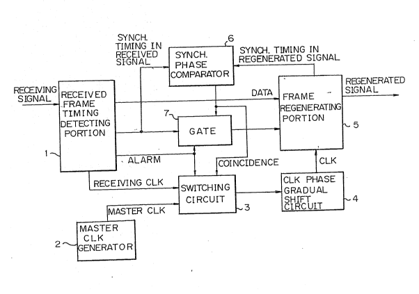
Pigure 2 shows the basic construction of a
repeater according to the present invention.
In Fig. 2, reference numeral 1 denotes a received
frame timing detecting portion, 2 denotes a master clock
generator, 3 denotes a switching circuit, ~ denotes a
clock phase gradual shift circuit, 5 denotes a frame
regeneration portion, 6 denotes a frame synchronization
phase compar~ator, and 7 denotes a gate.
The received frame timing detecting portion 1
extracts a receiving clock from a received frame-
multiplexed signal, detects a timing of frame
synchroni,zation in the received signal, and outputs an
alarm signal which indicates whether or not the timing
of frame synchronization is successfully detected.
The master clock generator 2 generates a master
clock.
The frame synchronization phase comparator 6
detects a coincidence between the timing of frame
synchronization detected in the recei~ed signal and a
timing of frame synchronization in a regenerated frame-
multiplexed signal.
The suitching circuit 3 outputs the receiving
clock except, the output of the switching circuit 3 is
switched to the master clock when the alarm signal
indicates~ a failure of the detection, and the output is
switched back to the receiving clock when the alarm
signal indicates a successful detection of frame
synchronization and the coincidence is simultaneously
detected.
The clock Phase gradual shift circuit 4 receives
the outpu~t of the switching circuit 3 as an input clock,
outputs an output clock synchronized with the input
clock exce~pt that a phase shift resulting from an
3~ abrupt phase shift occurring in the input clock,
gradually appears in an output clock after the abrupt
phase shift in the input clock.
~3~7~
g
The frame regenerating portion 5 receives the
output of the clock phase gradual shift circuit 4 as a
clock, determines the timing of frame sYnchronization in
a regenerated frame-multiplexed signal, and regenerates
the frame-multiPlexed signal corresponding to the
received signal, wherein the timing of frame
synchronization in the regenerated frame-multiplexed
signal is synchronized with the timing of frame
synchronizati,on detected in the received signal when
the timing of frame synchronization is supplied, and the
timing of frame synchronization in the regenerated
frame-multiplexed signal is generated from the outPut of
the clock,phase gradual shift circuit ~ when the timin~
of frame synchronization is not supplied.
The gate 7 receives the timina of frame
synchronization detected in the received signal and
supplies the timing of frame synchronization only when
tha alarm signal indicates a successful detection and
the coincidence is simultaneously detected.
Therefore, according to the above construction,
first, an abrupt Phase shift in the input clock in the
frame regeneration portion, which may occur when the
input clock is switched from one to another, is
eliminated by the clock phase gradual shift circuit ~.
Further, when frame synchronization in the
received signal recovers from a failure of detection of
the timing of frame synchr.onization, in the above
construction, generally, a clock output at the
switching circuit is not switched to the receiving clock
immediately, and the timing of frame synchronization
detected in the received signal is also not supplied to
the frame regenerating portion 5 through the gate 2
immediate~ly. Thus, when a coincidence between the timing
of frame synchronization detected in the received
signal and the timing of frame synchronization in the
regenerated signal is detected in the synchronization
signal phase comparator 6, the clock output at the
,
-`` 13~ 7~
-10-
switchin~ circuit 3 is switched to the receiving clock,
and the timing of frame synchronization detected in the
received signal is supplied to the frame regenerating
portion 5 through the gate 2.
Therefore, no phase shift arises in the timing of
frame synchronization in the frame regenerating portion
5 even when the timing is changed from the timing
generated from the master clock CLK~ to the timing of
frame synchrpnization which is supplied from the
received frame timing detecting portion 1.
Through the above operation according to the
p~esent invention, conventional factors which may cause
a loss of~ frame synchronization, are eliminated.
Figure 3 shows the construction of an embodiment
of the present invention.
In ~ig. 3, reference numeral 14 denotes a clock
phase gradual shift circuit, 16 denotes a
synchronization signal phase comparator, 23 denotes a
switching control circuit, and 17 denotes an AND gate.
All of the other components shown in ~ig. 3 are the
same as the corresponding components shown in Fig
having the same denotation.
In the construction o~ Fig. 3, the aforementioned
framejsynchronization signal generated in the frame
regenerating circuit 15 (hereinafter called regeneration
frame synchronization signal, and denoted by SY~C2) is
output from the frame regenerating circuit 15 and is
then inPut into one of the input terminals of the
synchronization signal phase comparator 6. The received
frame synchronization signal SY~C1 is input into the
other input terminal of the synchronization signal phase
comparator 6. The output of the synchronization signal
phase comparator 6, denoted by S6, is applied to one
input terminal of the switch control circuit 23, and
becomes ON when the received frame synchronization
signal SY~C1`and the regeneration frame synchronization
signal SY~C2, coincide.
~ 3 ~
-11-
The aforementioned alarm signal ALR~ is applied to
the other input terminal of the switch control circuit
23. The alarm signal ALRM is also applied to one input
terminal of the A~D gate 17. The other two inputs of the
AND gate 17 are the received frame synchronization
signal SYNC1 and the output of the switch control
circuit 23. The output of the A~D gate 17 is supplied to
the frame regenerating circuit 15. The AND gate 17 and
the switch cqntrol circuit 23 correspond to the gate 7
shown in Fig. 2. The switch control circuit 23 is
realized by an AND gate.
The~output of the switch control circuit 23 is
also applied to a control input terminal of the
selector switch 13. The output of the selector switch
13 is input into the clock phase gradual shift circuit
14.
The function of the clock phase gradual shift
circuit 14 is the same as the corresponding circuit 4
shown in Fi8. 2. The output of the clock phase gradual
shift circuit 14, which is denoted by CLK~, is
supplied to the frame regenerating circuit 15.
Figure 4 shows a block diagram of an example of
the clock phase gradual shift circuit 4 in Fig. 2 or 14
in Fig, 3.
In Fig. 4, reference numeral 41 denotes a phase
comparator, 42 denotes a low pass filter, 43 denotes a
voltage controlled oscillator, and 44 denotes a
frequency divider.
As can be seen,the construction of ~ig. 4 is a
well-known phase-lock loop (PLL) circuit, and the PLL
circuit can realize the aforementioned function of the
clock~phase gradual shift circuit 4 in Fig. 2. The
initial phase dîfference between the receiving clock
CLKi and the master clock GLK~ is detected in the
phase comparator 41 as an abrupt phase shift of the
input clock, and a control to gradually decrease the
phase shift detected in the phase comparator 41 is
~3~ 7~
-12-
carried out through the loop construction of the phase
comparator 41, the low pass filter 42, the voltage
controlled oscillator 43 and the frequency di~ider 44.
According to the gradual decrease of the phase shift,
the frequency of the output CLKx of the PLL circuit
gradual 1Y approaches the frequencY of the master Glock
CLXM. as shown in Fig. 5.
~ igure 6 shows the construction of an example of
the s~nchronization signal phase comparator 6 in Pig. 2,
or 16 in ~ig. 3.
In Fig. 6, reference numeral 61 denotes a delay
circuit, and 62 denotes a D-type flip-flop circuit.
The,delaY circuit 61 delays the timing of the
input signal by on half of the clock period ~. The
received synchronization signal SYNCl is input into the
delay circuit 61, and the output, which is denoted by
SYNC1D, is applied to the D input terminal of the D-type
flip-flop circuit 62. The regeneration synchronization
signal SYNC2 is applied to the edge trigger input
terminal of the D-type flip-flop circuit 62.
Figure 7 shows the timing of the above signals
when the coincidence between the received
synchronization signal SYNCl and the regeneration
synchronization signal SYNC2 is detected. NamelY, ~hen
the above two signals SYNCl and SYNC2 coincide, the
delayed signal SY~GlD is always at the LOW level at the
timing of the leading edge of the signal SYNC2, and
therefore, the output of the synchronization signal
phase comparator, which is the inverted output, is HIGH.
When the abo~e two signals SYNC1 and SYNC2 do not
coincide, the output of the synchronization signal
phase comparator is LO~.
Figure 8 shows the timing of the construction of
~ig. 3. At time tl, frame synchronization in the framc
synchronization circuit 11 has failed. Immediately the
frame synchronization signal SYNC1 is stopped at the
A~D gate 17 and the alarm signal ALRM becomes LOW.
13~7t~
-13-
Therefore the output of the switch control circuit 23
becomes LOW, and the output clock of the selector switch
13 is then Sh`i tched from the receiving clock CLKi to
the master clock CLUM. As mentioned above, the phase
and the frequency of the output CLKx of the clock phase
gradual shift circuit 14 is gradually shifted to
coincide with the master clock CLK~ and reaches
coincidence at the time t2.
At tim;e t3, frame synchronization in the frame
synchronization circuit 11 has recovered. However, at
this time, the output signal S6 of the synchronization
signal phase comparator is LOW, i.e., the frame
synchroni,zation signals SYNCl and SYNC2 do not coincide.
Since the freguencies of the receiving clock CLKi and
the master clock CLKM are different, the frame
synchronization signals SYNC1 and SYNC2 coincide at an
interval determined by the frequency difference.
- Therefore, after an interval, at time t4, the output
signal S6 of the synchrPnization signal phase
comparator becomes HIGH. Accordingly, the output of the
switch control circuit 23 becomes HIGH, and thus the
frame synchronization signal SY~Cl is applied to the
frame regenerat;ng circuit 15 through the AND gate 17,
and the output clock of the selector switch 13 is
switched back to the receiving clock CLKi.
.~gain, as mentioned above, the phase and the
frequency of the output CLKx of the clock phase
gradual shift circuit 14 is gradually shifted to
coincide with the receiving clock CLK;, and reaches
33 coincidence at the time t5, thus returning the repeater
to the normal state.
As shown in Fig. 8, the phase and frequency of the
clock supplied ~o the frame regenerating circuit always
changes gradually, and the timing of the change of the
frame synchronization signal SYNG2 from the timing
generated from the master clock C~KM to the timing
synchronizing with the frame synchronization signal
:
''' , : ' '
`' ' , ,,~
~3~7~
-14-
SY~'C1, is also carried out continuously, i.e., with no
phase shift
Thus, according to the present invention, the
occurrence of a loss of frame synchronization can be
avoided.