Note: Descriptions are shown in the official language in which they were submitted.
13~73~9
20365-2~83
SWITC~ING NODE FOR SWITCHING DATA_SIGNAI.S TRANSHITTED IN DATA
PACKETS
The present invention relates to a switchlng node for
switching data 3ignals transmitted in data packets each of which
includes an address signal. The switching node lncludes at least
one coupling element which has a plurality n of input lines
selectably coupled to said input lines via a space switch. A
plurality n of buffer stores each are respectively connected
between a particular one of the input lines and the space switch,
in each of which a plurality k of data packets occurring
sequentially on the particular input line are storable before
being routed further to an output line indicated by the address
signal contained in the particular data packet.
In known switching nodes such as are known from, for
example, U.S. Patent ~,491,945, issued January 1, 1985 to Turner,
the buffer stores assigned to the input llnes have in each
instance only a single output termlnal. Because of thls, at any
given point ln tlme, a data packet can only be transferred from
the buffer store to the space switch. This results ln dlfferent
waiting tlmes (before belng swltched) for the individual data
packets recelved in a buffer store as a function of the number of
prevlously received data packe~s. These waiting times vary
widely, especlally lf data packets with variable length are
switched vla the swltching node.
It is desirable that a switching node of the above-
described type be able to decrease the previously mentioned
13173~9 203~5-2883
waiting times, and the waiting time fluctuations for the data
packets stored in the buffer stores.
In ac~ordance with the present invention, a switching
node of the above type has a space switch having a plurality m x n
of input terminals connected respectively to the corresponding m
output terminals of the n buffer stores, and a plurality n of
output terminals connected respectively to the n output lines.
The buffer stores each having a plurality m c k of output
terminals connected respectively to the corresponding m input
terminals of said space switch for each particular buffer store
via which m data pac~ets stored in the particular buffer store can
be routed further to m different output lines by being
simultaneously suppliable to the m input terminals of the space
switch.
1 3 1 7 3 ~ 9 20365-2883
A switching node in accordance with the present inven-
tion has the advantage that the transit time of the data packets
or the fluctuations of the transit time through the switching node
due to the waiting time of the data packets in the individual
buffer stores, is reduced. This is because a plurality of data
packets can simultaneously be supplied to the space switch from
the individual buffer stores.
In the drawing:
Figure 1 is circuit block diagram of a coupling element
in accordance with the present invention;
Figure 2 is a more detailed circuit block diagram of a
buffer store, and a buffer store control device connected to it,
which may be used in the coupling element illustrated in Figure l;
Figure 3 is a timing diagram useful in understanding
the operation of the coupling element illustrated in Figure l; and
Figure 4 is a circuit block diagram of a central con-
trol device which may be used in the coupling element illustrated
in Figure 1.
In Figure 1 a coupling element of a switching node is
represented in the form of a block circuit diagram. Only those
circuit parts required for comprehension of the present invention
are shown.
The coupling element has n input lines El to En of
which only input lines El and En are shown. The input lines may
be connected with terminal devices (not shown) or with output lines
transmitting data packets from one or several upstream coupling
~ 3 ~ 7 3 5 9 20365-2883
elements of the switching node (also not shown). Each of the
input lines (El to En) is associated with a buffer store in which
k successive data packets can be stored. The buffer store
associated with the input lines El and En is designated by PSl and
PSn, respectively. Each of the buffer stores (PSl to PSn) is
controlled by a respective buffer store control device connected
to the associated input line. The buffer store control device
assigned to buffer stores PSl and PSn is designated PSSl and PSSn,
respectively. Each of the buffer store control devices (PSSl to
PSSn) has a control line which, for the buffer store control
devices PSSl and PSSn, is designated SEl and SEn, respectively.
The buffer stores PSl to PSn each have a plurality of
m ~ k outputs terminals, designated 1, ... m, which are routed to
a space switch RK. This space switch is provided with m x n input
terminals, corresponding to the n x m output terminals of the
buffer stores, and n output terminals, connected to output lines
Al to An which may be connected to end devices (not shown) for
receiving data packets or to input lines of one or several down-
stream coupling elements of the switching node (also not shown).
A plurality of control lines, which are designated SAl to SAn,
are respectively associated with the output lines (Al to An) of
the space switch.
To control the setting of the space switch RK, a central
control device ZST is connected to it via two unidirectional bus
line systems BUSl and BUS2, for example, in the form of a micro-
processor configuration. This central control device ZST, in
-- 4 --
1 3 1 7 3 ~ 9 20365-2883
addition, is connected via a bidirectional bus line system sUS3
to the buffer store control devices PSSl through PSSn~
In operation, the assumption is made that each of the
data packets supplied to the coupling element by the individual
input lines El through En is associated with a virtual connection
and includes an address signal which designates the output line of
the coupling element selected for the particular virtual connec-
tion. These data packets may optionally be preprocessed approp-
riately by, for example, devices preceding the coupling element.
The individual data packets may be variable with respect to their
length up to a predetermined maximum length.
The data packets supplied sequentially to the coupling
element, for example, by the input line El, are placed into
intermediate storage in buffer store PSl before being routed
further by the coupling element. This temporary storage takes
place under the control of buffer store control device PSSl which,
upon the arrival of a data packet, selects a free storage area of
buffer store PSl for the temporary storage of the particular data
packet. After the temporary storage of a data packet in the
buffer store PSl, the buffer store control device PSSl supplies
the address signal included in this data packet, together with
the address of the storage area in which the just received data
packet is stored, to the central control device ZST, via the bus
line system BUS3.
The same processes also take place in the remaining
buffer stores (PS2 to PSn and buffer store control devices (PSS2
1 31 7359 2036~-2883
to PSSn) with respect to the intermediate storage of data packets
arriving on input lines E2 to En, respectively.
The central control device ZST manages the data packets
waiting in the buffer stores PSl to PSn (to be routed further via
the space switch RK) on the basis of the information transmitted
to it by the individual buffer store control devices PSSl to PSSn.
Further routing of the data packets via the space switch RK takes
place synchronously. Successive time intervals are defined
determined initially by packet clocks. These intervals may cor-
respond, for example, to the maximum time duration of a data
packet of the predetermined maximum length. The central control
device ZST, in response to the information supplied to it by the
buffer store control devices PSSl to PSSn, selects n data packets
for routing to the n output terminals of the space switch RK. The
space switch is correspondingly set via the bus line system BUSl.
To this end, n selected input terminals of the m x n total
available input terminals of space switch RK are connected by
cross-points to corresponding output lines Al to An.
After setting space switch RK, the central control
device ZST then sequentially sends to the appropriate buffer store
control devices (PSSl to PSSn), at a time determined by a packet
clock, the storage addresses in the associated buffer stores at
which the selected data packets are stored, via BUS3. A buffer
store control device (PSSl to PSSn) may receive up to m storage
addresses, corresponding to the number of output terminals of the
associated buffer store. The particular buffer store control
1 3 1 7 3 5 9 20365-2883
device (PSSl to PSSn) accesses its associated buffer store (PSl to
PSn, respectively) according to the storage address or storage
addresses which the associated buffer store control device (PSSl
to PSSn) received. The buffer control device (PSSl to PSSn) then
causes the buffer store ~PSl to PSn) to transmit one or several
data packets, through an appropriate number of read commands.
The output terminal of the buffer store (PSl to PSn) to be used
for each of the transmitted packets is determined from information
from the central control device ZST included with each of the
storage addressses. The control of the further routing of data
packets by the central control device ZST takes place in such a
manner that the sequence of the arrival of the individual data
packets is taken into consideration. In this manner, a loss of
data packets or unordering of sequential data packets belonging
to a single virtual connectlon is avoided.
The central control device ZST, furthermore, also
manages the work-load of the individual buffer stores PSl to PSn.
For example, upon reaching a predetermined level of filling of one
of the buffer stores (for example, of buffer store PSl)~ the
central control device ZST conditions the buffer store control
device associated with the particular buffer store (for example,
the buffer store control device PSSl), to produce a control signal
on the associated control line (SEl). Through such a control
signal, the device connected with the particular input line for
example, El), is conditioned to temporarily interrupt the trans-
mission of an~v further data packets. The reception of data
1 3 1 7 3 ~ 9 20365-2883
packets by the particular buffer store may be renewed, for
example, through the removal of the just cited control signal.
The central control device ZST also receives control
signals occurring on the already stated control lines SAl to SAn
from the space switch RK via the bus line system BUS2. The control
signals indicate that transmission of a data packet the associat-
ed one of the output lines Al to An is not possible due to an
overload of the receiving device connected to the particular output
line. As mentioned above already, such a device may be either an
end device or a succeeding coupling element of the switching node.
Above, the assumption was made that each of buffer store
PSl to PSn has m 6 k output terminals. If the number of output
terminals per buffer store is selected to be, for example, m = 2,
then the capacity of the described coupling element to put data
packets through can be increased by between 60% to 90% compared
to a coupling with buffer stores each having only one output
terminal. This through-put capacity, however, can be increased
still further by further increasing the number of output terminals
per buffer store.
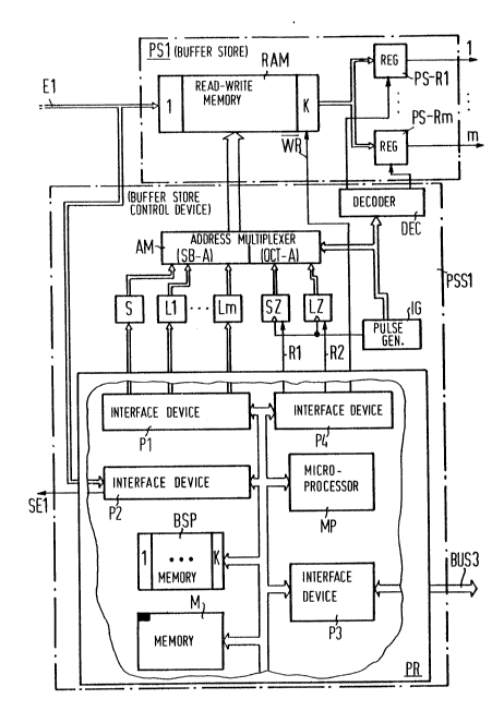
In Figure 2, a possible structure of a buffer store and
buffer store control device, as illustrated in Figure 1 is given
using the buffer store PSl and the buffer store control device
PSSl as example. It is assumed that, as already mentioned above,
the individual data packets are preprocessed by a device preceding
the buffer store in such a way that each has an address signal
included with it through which one of the output lines of the
20365~2883
~31735~
coupling element is designated. The input line El, connected to
buffer store PSl and shown only schematically in Figure 1, may
be implemented as a multibit digital bus line with a plurality of
individual lines of which a first portion is used for transmis-
sion of sequential eight bit bytes of the data packets and
another portion for the transmission of the address signals.
The buffer store PSl has a read-write (random access)
memory RAM which is connected on the input-side to the portion of
the individual lines of the multibit digital bus line El carrying
the 8 bit bytes of the data packets. This RAM contains a total
of k storage areas, which may be numbered 1 to k, in each of
which 8 bit bytes of a data packet can be stored in successive
storage cells. On the output side of the read-write memory RAM,
m parallel-to-serial registers PS-Rl to PS-Rm are connected.
These registers, which form the output terminals 1 to m of buffer
store PSl (as illustrated in Figure 1), are accessible individual-
ly via a respective control input terminal, and receive an 8 bit
byte from the output terminal of the read-write memory RAM, which
was produced by a read process of the read-write memory RAM. As
will be explained below, in the course of a single control cycle,
an 8 bit byte can be received into each of the m parallel-to-serial
registers. These 8 bit bytes are subsequently simultaneously
further routed serially to the space switch RX.
To control of the read-write memory RAM, an address
multiplexer AM in the buffer store control device PSSl is connec-
ted to the address input terminals of the read-write memory RAM.
_ 9 _
1 ~ 1 7 3 ~ ~ 20365-2883
This address multiplexer AM is subdivided into two sections: SB-A
and OCT-A. Connected to section SB-A is a register S, for storing
a store area address to be used for write processes, and m regis-
ters Ll to Lm, for storing respective storage area addresses to
be used for read processes. Registers Ll to Lm are associated with
the buffer store PSl output terminals labeled 1 to m, respectively.
To section OCT-A is connected, in contrast, a byte counter SZ,
for write processes, and a byte counter LZ, for read processes.
These 8 bit byte counters each have a counting period correspond-
ing to the maximum number of 8 bit bytes contained in a datapacket and are clocked by a pulse generator IG. This pulse
generator, moreover, also supplies the address multiplexer AM and
a decoder DEC with setting signals in the course of a control
cycle. Decoder DEC has m output terminals which are connected to
the above cited control input terminals of the parallel-to-serial
registers PS-Rl to PS-Rm.
Buffer control device PSSl, also includes a processor PR
which is formed, for example, from a microprocessor configuration.
This microprocessor configuration includes a microprocessor MP to
whose bus system a storage arrangement comprising the memories
BSP and M as well as four interface devices Pl to P4 are connected.
Memory M functions in known manner as working and program storage.
Memory BSP includes storage cells 1 to k in which are stored the
actual states of occupancy of storage areas 1 to k of the read-
write memory RAM are stored.
At the interface device Pl, the previously cited
-- 10 --
1317359 20365-2883
registers S and Ll to Lm are connected at the input side. Inter-
face device P2 is connected to the multibit parallel digital line
El, and to the line SEl, given in Figure 1. The buffer store
control device PSSl is coupled to the bus line system BUS3
(represented in Figure 1) via interface device P3. Lastly, from
interface device P4, a line denoted by WR is coupled to the read-
write memory RAM, and reset lines Rl and R2 are coupled to 8 bit
byte counters SZ and LZ, respectively. Write pulses are sent to
read-write memory R~M via the WR line.
In the previously described memory sSP, the actual
occupancy of the storage area of the read-write memory RAM is
stored. On the basis of this occupancy information, the micro-
processor MP determines a non-occupied storage area in which a
data packet occurring subsequently on multibit digital signal line
El is to be stored. The starting address of this storage area is
subsequently sent into register S.
Upon the occurrence of a data packet on multibit
digital signal line El, which is recognized by the microprocessor
on the basis of the packet head, the already cited pulse generator
IG sends a setting signal to the address multiplexer AM via a line
configuration S. Through this setting signal, the address multi-
plexer AM iS controlled in such a way that it supplies the pre-
viously cited starting address stored in register S and an initial
count of 8 bit byte counter SZ to the read-write memory RAM as
address signals. This initial counter count is set through a
reset signal on reset line Rl. In addition, microprocessor MP
~. 3 1 7 3 ~ 9 20365-2883
sends write pulses to the read-write memory via line WR. On the
basis of the occurrence of these write pulses, and an incrementa-
tion of the actual counter count of 8 bit byte counter SZ
connected therewith, the individual 8 bit bytes of the just
occurring data packet are stored sequentially in storage cells of
the read-write memory. After complete storage of the data packet,
the memory BSP, present in processor PR, is updated and, in
preparation for the renewed reception of a data packet, a start-
ing address of a free storage area of the read-write memory RAM
is sent into register S. Moreover, as already stated above, the
address signals included with the data packet on multibit digital
signal line El and the starting address of the just used storage
area of the read-write memory RAM are routed to the central
control device ZST via the bus line system BUS3.
Furthermore, as mentioned above, the central control
device ZST, at fixed ~ime intervals, successively routes n control
data signals to selected buffer store control devices (PSSl to
PSSn) via the bus line system BUS3 in order to include each
associated buffer store in a transmission of data packets via the
~0 space switch RK. Each of these control data signals includes the
starting a!d~ress of that storage area of the read-write memory
RAM in which the data block to be transmitted is stored. The
control data signals also contains the output terminal of the
particular buffer store to be used for the transmission. For
example, the buffer store control device PSSl shown in Figure 2
may receive up to m control data signals corresponding to the
1317359
20365-28~3
number of output terminals present in the associated buffer store
PSl. upon reception of these control data signals, the cited
starting addresses are sent, on the basis of the output terminal
selection, into registers Ll to Lm.
Subsequently, a control cycle is carried out by the
buffer store control device PSSl which extends over the duration
of the just started time interval and is subdivided into a number
of subcycles corresponding to the maximum number of 8 bit bytes
which may be contained in a data packet. In each of these sub-
cycles setting signals are successively routed from pulse
generator IG to the address multiplexer AM and the decoder DEC
via the line configuration S. Through these setting signals the
starting addresses stored in registers Ll to Lm and the current
counter count of 8 bit byte counter LZ are made available as
address signals to the read-write memory RAM for reading out 8 bit
bytes in time division multiplex operation. The 8 bit byte counter
assumes its initial counter count at the beginning of the con~rol
cycle through a reset signal on reset line R2. At the end of such
subcycle then, starting from the initial counter count, the
current counter count is incremented.
In each of the ~ust described subcycles, m 8 bit bytes
are read out from m different data blocks and supplied to the
parallel-to-serial registers PS-Rl to PS-Rm. These registers are
activated successively via decoder DEC for the reception of an 8
bit byte. After receiving this 8 bit byte, a simultaneous serial
transmission to the space switch RK takes place.
- 13 -
~3173~ 20365-2883
The remainder of the previously described control
cycle is so defi.ned that in each subcycle an 8 bit byte of a data
packet occurring on multibit digital signal lines El can also be
written into the read-write memory RAM. This is apparent in the
time diagram i].lustrated in Figure 3. In Figure 3, two successive
subcycles p and p+l are illustrated. The top line shows the
current count q and q+l of 8 bit byte counter SZ. The next line
shows the current count r and r+l respectively of 8 bit byte
counter I,Z. The next line shows the address signals occurring at
the output terminals of section SB-A of the address multiplexer
AM; and the next line shows the address signals occurring at the
output terminals of section OCT-A of the address multiplexer AM.
The relative position in time of a write pulse WR and setting
signals El to Em occurring on line configuration S are shown on
the remaining lines.
In Figure 4 a possible structure of the central control
device ZST, as illustrated in Figure l, is represented in block
diagram form. In Figure 4, the central control device includes a
microprocessor MPl to whose bus system two interface devices P5
and P6, and a storage arrangement comprising a memory Ml and a
read-write memory PS-M are connected. The interface device P5 is
provided for a data exchange with the buffer storage control
devices PSSl to PSSn via the bus line system BUS3. Via the inter-
face device P6, in contrast, the central control device ZST is in
connection with bus line systems BUSl and BUS2.
Memory Ml functions in known manner as working and
- 13a -
1 3 1 7 3 ~ 9 20365-2883
program storage. The above described control of the transmission
of data packets waiting in the individual buffer stores (PSl to
PSn) takes place with the aid of store PS-M. Store PS-M has
storage areas l to n corresponding to the n buffer stores PSl to
PSn. Each of these store areas is subdivided into k + l storage
cells corresponding to the data packets storable in the buffer
stores. The first k storage cells provide storage for the address
signals included with the data packets supplied by the particular
buffer store control device. For this storage, which may be car-
ried out, for example, according to a list of free storage cells
maintained in store Ml, a cell part, denoted by ADR, is provided
in each of the k storage cells. In a further cell part, denoted
by RF, the sequence of arrival of the individual address signals
and, hence, the sequence of the data packets received into the
particular buffer store is marked. This sequence is updated with
each read and write by address signals, for example, according to
a known concatenation principle.
In the last of the k+l storage cells of a storage area
the instantaneous state of occupancy of the particular storage area
and, hence, the state of occupancy of the particular buffer store
is stored.
On the basis of the information deposited in the just
described storage PS-M the microprocessor associated with the
central control device ZST selects, at successive intervals, n data
packets for further routing to the n output terminals of the
space switch RY. As a function of the work-load of the individual
- 13b -
1 3 1 7 3 ~ 9 20365-2883
output terminals of the space switch, up to m data packets stored
in the same buffer storage may be taken into consideration.
~fter such a selection, subsequently, a setting of the space
switch RK in -the above stated manner and a routing of control data
signals to the possible buffer store control device takes place.
- 13c -