Note: Descriptions are shown in the official language in which they were submitted.
~ 3 ~ , E5-006
--2--
This invention relates to method and apparatus for
reading an image recorded electronically on a recording
surface. It relates more particularly to a read-out system
for producing signals representative of electronic patterns
stored on a movable electronic storage medium.
sack round of the Invention
There presently exist electronic devices such as
vidicons which use an electron beam to detect the presence
of optical or electronic signal patterns on a recording
surface. Depending upon the particular application, these
devices use different means for focusing and deflecting the
electron beam, as well as for collecting the signal currents
representative of the electronic pattern recorded on the
recording surface. All of these devices have three things
in common, namely (1) a cathode which emits the electron
beam, (2) a recording surface which is able to sense an
optically induced electronic resistance pattern, and (3)
collector means for collecting a signal current resulting
from the scanning of the optically induced pattern by the
beam.
1 3 ~ ; E5-006
--3--
In a typical vidicon, the recording surface is a
transparent metallic plate on the face of the vidicon tube,
one side of which is coated with a thin layer of
photoconductor material. The optical image is focused onto
the photoconductor material layer and is scanned with an
electron beam originating at a cathode spaced from the tube
face while the optical image persists. The scanning beam
deposits electrons on each scan spot so as to generate a
current to ground whose magnitude corresponds to the change
in resistance of the photoconductor which, in turn, is
proportional to the intensity of illumination on said spot.
The current through a load resistor connected to the plate,
which constitutes the output of the vidicon, therefore,
reproduces the variations in the light intensity of the
successive portions of the optical image projected onto the
face of the vidicon.
Prior apparatus such as this for reading an image from
an electronic recording surface without making it visible
via electrotatic toner, but using a scanning electron beam
instead, are disadvantaged because the positions of the
electron beam source and the recording surface position are
fixed. Accordingly, only one image at a time can be stored
on the recording surface. In other words, in order to read
E5-006
--4--
an image from that surface, all previous images recorded
thereon will have had to be stored elsewhere so that the
recording surface can be erased. Therefore, electron
devices such as vidicons have limited application as means
for reading electronically stored images.
There have been some efforts in the past to develop a
recording medium or phototape which can store a plurality of
electronic images for later readout directly using a
scanning electron beam. Such a system is disclosed in the
publication Electrostatic Imaging and Recording hy E.C.
Hutter, et al, Journal of the S.M.P.T.E. Vol. 69, January
1960, pp.32-35. The recording medium or phototape in that
reference is also disclosed in U.S. Patent 3,124,456
(Moore). The medium comprises a transparent polyester base
coated on one side with a layer of photoconductive material
which is, in turn, coated with a thin layer of a dieletric
material. To record an image on that medium, the dielectric
layer is precharged by a voltage applied across that layer
and then the photoconductive layer is exposed to a light
image while an electric field is applied across the
dielectric layer. The charge in the dielectric layer decays
towards zero with the decay being most rapid where the
optical image is brightest and, therefore, the
~ 3 ~ E5-006
--5--
photoconducitve resistance is lowest. After a time
corresponding to the greatest difference between the
potentials in the light and dark areas of the medium, the
electric field is turned off and the discharging process
stops, thereby leaving on the dielectric layer an
electrostatic charge distribution corresponding to the
optical image incident on the medium. The stored image may
be read from the medium by scanning the dielectric layer
with a focused electron beam to produce an electrical signal
corresponding to the stored image.
The Hutter et al system has several disadvantages. It
can store acquired data in the recording medium for only a
limited period of time, e.g. a few weeks, because of charge
leakage in the dielectric layer of that medium. Also, the
medium has poor light sensitivity. Accordingly, the quality
of the images recorded on the medium is not very high. Most
importantly, readout of the image stored on the medium by
the scanning electron beam is accomplished by detecting a
capacitively modulated current signal from the medium
involving simultaneous movement of many charge carriers in
the medium. Resultantly, the resolution of the detected
picture signal is much less than that of the stored
~3~ E5-006
--6--
electronic image which, as just stated, was fairly poor to
begin with.
The ~utter et al system is disadvantaged also because
in the process of reading the stored images on the recording
medium using a scanning electron beam, those images are
rapidly degraded by the electron beam scanning process
itself because the beam electrons cause electronic
conduction in the medium. In other words, when that system
performs a read operation, it also tends to erase the images
stored in the medium. This, of course, is completely
unacceptable if that arrangement is to be considered for
storage of images which may have to be retrieved several
times during the storage period. Also, during the image
sensing operation, the photoconductive medium proposed by
Hutter is plagued by excessive dark currents which reduces
the signal detection threshold sharply.
Other systems which use a scanning electron beam to
read images on a movable storage medium are disclosed in
U.S. Patents 3,880,514 ~Kuehnle) and 4,242,433 ~Kuehnle et
al). Those systems are superior to the Hutter et al
recording system in that they do not require precharging of
the recording medium; otherwise they are disadvantaged in
the same respects. Indeed, all these prior systems are
~ 2`~i, ES-006
--7--
totally useless for long term storage of high resolution
image pattern, and for sensing signals at very low light
levels.
Summar of the Invention
Y
Accordingly, this invention aims to provide an improved
read-out system for producing signals representative of
electronic signal patterns stored on a movable electronic
storage medium.
Another objective of the present invention to provide
an electron beam scanning system having a recording surface
that is movable so that a plurality of images can be stored
simultaneously on the recording medium and be scanned
selectively by the beam.
Another object of the invention is to provide a system
of this type whose movable recording medium has a plurality
of imaging frames which can be positioned accurately for
scanning by the electron beam.
A further object of the invention is to provide an
electron beam scanning system whose beam has an auto-
positioning capability to achieve precise alignment of the
beam position and scan direction prior to commencing the
~ E5-006
--8--
scan, with respect to the electronic pattern stored on each
frame of the recording medium.
Yet another object of the invention is to provide such
a system whose image-representing output, produced during
the electron beam scanning process, has an unusually high
signal-to-noise ratio.
A further object of the invention is to provide an
electron beam scanning system which can read image-
representative electronic patterns on a recording medium
using a scanning electron beam in a manner that does not
degrade the stored patterns.
Yet another object of the invention is to provide a
system of the aforesaid type which achieves close control of
the electron beam scan path during the reading of an
electronic pattern stored on a recording medium.
Another object of the invention is to provide an
electron beam scanning system for reading images recorded
electronically on a recording medium that can operate with
minimal electrical power as compared with other image
sensing, storing and scanning devices.
A further object of the invention is to provide an
electron beam scanning system having a movable recording
~ 3 ~ ~ `}~ ~ ~i E5-006
_g_
member which can form the basis of a microscope, a camera or
even a digital signal storage memory unit.
Another important object of the invention is to provide
a reading process, which scans the storage medium with one
or more sensing needles capable of detecting tunneling
electrons when a voltage is applied between the medium and
each needle, with the number of electrons being modulated by
the imagewise field pattern on the medium at that location.
Still another object of the invention is to provide
methods of retrieving or reading electronic images stored on
a movable recording medium that produce one or more of the
aforesaid advantages.
Other objects will, in part, be obvious and will, in
part, appear hereinafter.
The invention accordingly comprises the several steps
of the relation of one or more of such steps with respect to
each of the others, and the apparatus embodying the sequence
of steps and the features of construction, combination of
elements and arrangement of parts which are adapted to
effect such steps, all as exemplified in the following
detailed description, and the scope o the invention will be
indicated in the claims.
1 ~ 6``442l-4lo
sriefly, my electron beam scanning system includes an
electron beam source or an array of current detecting needles, an
optoelectronic recording member having a plurality of image ~rames
for storing electronic patterns and a collection means for
electron emissions which represent the information signals. The
recording member can be moved relative to that source to position
the image frames selectively for scanning by the electron beam in
order to read the images stored on those frames. Preferably, the
recording member incorporates the plural-layer, solid state,
wholly inorganic, wholly crystalline, optoelectronlc recordlng
medlum dlsclosed in my U.S. Patent No. 4,862,414. That medlum
includes a transparent inorganic bAse, a photoconductive modulator
on the base and a dual-materlal dielectric storage layer on the
modulator. It can be controllably and simultaneously
electronlcally charged and exposed so that the medlum acqulres and
stores ln its storage layer an electronic charge pattern
correspondlng to the image pro~ected onto the medlum. Preferably
also, the recording member ls ln the form of a tape, although it
could ~ust as well be a disc, drum or plat~, havlng sufflcient
~3~ rl~j ES-006
--11--
surface area to accomodate at least a plurality of, and
preferably many, separate recording areas or frames, each
capable of acquiring and storing an image-representing
electronic pattern. The storage member is movably
positioned within an evacuated housing so that it can be
shifted to position any selected frame at a write station or
at a read station also located within the evacuated housing.
At the write station, a selected frame on the tape is
positioned at a focal plane and exposed to an optical image
or signal projected onto that frame by projection optics
mounted in the wall of the housing. While the tape frame is
being exposed to the incoming optical signal, an electron
source at the write station deposits a cloud of electrons on
the surface of the tape's dielectric storage layer thus
creating a virtual, momentary electrode. At the same time,
the active layers of the tape are subjected to a very
intense electric field caused by the electron deposition on
the surface of the dielectric storage layer and a counter-
potential at an electrode layer beneath a light modulating
photoconductive layer comprising the modulator, that
electrode layer being placed directly on the base or support
substrate of the tape. The energy in the light image
focused onto the tape frame is absorbed in the
~ 3 ~ ~ ~ 7 E5-006
-12-
photoconductive layer or zone, thereby creating electron-
hole pairs in that photoconductor. Under the influence of
the field, which is established between the two electrodes,
the positive carriers or holes created by the light will
tunnel through an interface or barrier zone (field effect)
comprising one component of the dual-material storaqe layer
and penetrate the underside of the other storage layer
component, namely the dielectric storage zone forming there
so called charge centroids, while the negative charges or
electrons are conducted away from the photoconductive zone
via the electrode to an external battery. The positive
charges become trapped or "pinned" to the underside of the
dielectric storage zone and as soon as the electric field is
turned off, the interface zone acts as a barrier to prevent
any thermally-generated or image-unrelated photogenerated
charges from tunneling through the interface zone and thus
accidently neutralizing the positive, image-related charges
which are pinned, as charge centroids, at the underside of
the dielectric storage zone. To keep positive charges from
emanating at the electrode and being injected into the
photoconductor, the electrode is typically made of an n-type
structure.
~ '?j'' E5-006
-13-
While the image projected onto the tape frame at the
write station may be a black and white image, preferably it
is a color image produced by passing the imaging light
through an array of alternating, thin, horizontal red, green
and blue filter stripes (or a diffraction filter) present on
a platen in the focal plane or on the tape itself. Thus the
charge pattern applied to the tape frame consists of
interlaced red, green and blue color components of the image
projected onto the frame. In other words, the picture
information for each color component of the picture is
stored every third line on the tape frame.
Simultaneous with the recording of the picture on the
tape frame, a precise electronic fiducial mark is recorded
in that frame outside the image area of the tape. This
fiducial mark enables the system, prior to each read out
operation, to set the initial or '`home" position and skew of
the scanning electron beam from the electron beam source or
needle array sensor to compensate for any slight
mispositioning of the tape rame at its position in the read
station when the electronic image thereon is being read from
the frame by the scanning electron beam with respect to its
position at the focal plane in the write station when that
image was recorded on that frame.
~ ES-006
-14-
My system may also include provision for automatically
focusing the image projected onto the frame at the write
station and for setting automatically the charging current
applied to the tape's electrode layer in accordance with the
intensity of the incoming light in order t~ control
automatically the frame exposure. In fact, the tape and the
remaining elements of my system interact and cooperate
optically and electronically to optimi2e the exposure of the
tape under the prevailing light conditions at the write
station so that the image recorded on the tape frame is at
the highest resolution and has many steps of gray (dynamic
range) and large contrasts. The electronic pattern recorded
on the tape frame corresponds to an optical image that is
finely focused and the image-representing charges stored at
different locations on the tape frame may vary from as few
as 20 electrons/resolution element to 20,000 electrons/
resolution element. This charge difference yields a dynamic
range in the stored imaqe of 1,000:1, permitting easily the
retrieval of 32 or more different gray levels in the image
recorded on the tape frame.
In the present system, the tape is moved between the
write and read stations by a pair of motor-driven spools,
with the tape being guided along a focal plane at the write
3~ E5-006
~c3 _~s
-15-
station and along a scanning plane at the read station. The
motors are controlled by the system controller in response
to signals from a pair of frame position detectors at the
write and read stations which sense position marks denoting
the location of each image frame on the tape. By counting
position signals from these detectors, the system controller
"knows" when any selected frame is located at the write
station and when that frame is positioned at the read
station, and it also is able to maintain a count of the
frame number.
When it is desired to retrieve an image previously
recorded on a particular image feame of the tape at the
write station, the controller activates the tape drive
motors to position that selected frame in the scanning plane
at the read station. After the position detector there
detects the position mark corresponding to that frame, it
issues a control signal to the system controller which
thereupon stops the tape drive motors so that the frame is
centered in the scanning plane as accurately as possible
within allowable mechanical tolerances.
An electron beam source at the read station then
directs a beam of electrons to the dielectric layer of the
tape frame present at the scanning plane to seek an
E;5-006
-16- ~ ~ ~ r~
electronic position/fiducial mark so that the beam can lock
the sweep control electronics into a "zero-setting" scan
position thereby initiali~ing the read operation. Then, the
electron source is controlled so that the electron beam
sweeps out a parallel raster on the dielectric surface of
that frame. If the electronic pattern on the frame
represents a color image, the raster lines should correspond
to lines on the frame that were exposed through the array of
parallel, horizontal filter stripes at the write station.
Preferably also, the beam source cathode consists of a cold
field emission source rather than a thermoionic source
because the former requires less power and does not generate
infrared emission so that the tape frame present at the read
station is not exposed to perceptible light radiation.
Such radiation would degrade the electronic image stored on
the tape during read-out because the tape is sensitive to
infrared radiation.
During read--out, the information contained on the tape
frame at the read station is not retrieved by detecting a
capacitively modulated current signal from the tape in the
manner of conventional electronic beam scanning apparatus
described at the outset. Rather, during read-out, the
scanning electron beam in the present system, while finely
E5-006
-17- ~ r6~ ~ ;
focused, is capable of penetrating the tape~s insulating
storage layer with sufficient energy to generate the
secondary emission of electrons from beneath the surface of
the insulator. The electronic image or signal pattern is
represented by field domains across the insulator thickness
whereby the positive charges sit well beneath the
penetration depth of the electron beam and, therefore,
remain unaffected by the scan beam. Accordingly, the
scanning of the tape by the beam does not erase the stored
signal pattern or image. Repeated scanning of the medium by
the primary beam does cause unimaged areas of the medium
surface to become progressively more positive. This
unbalance may be removed and the surface replenished with
negative charges by exposing the medium surface to a beam of
relatively low energy electrons either before or after the
medium is scanned for readout of image data.
The number of electrons in the secondary flux from each
resolution element scanned is measueed and compared to the
number of primary electrons, with the difference in flux
being the indicator and measure of the signal after
deducting the flux due to the coefficient of emission from
the neutral medium surface. Accordingly, the electrons in
the secondary flux from the tape have a numerical
~ J ~ J ~. ,,
E5-006
--18--
distribution by pixel or area element (resolution element)
that represents the total electronic image stored on that
frame. These emitted secondary electrons are collected by
an electron collector located at the read station which is
capable of literally counting the return flux electrons and
then amplifying them appropriately with a minimum of
electrical noise so that the system produces an output
signal which is the electrical analog of the electronic
pattern stored on that tape frame. The comparison of the
number of primary electrons to the larger number of
secondary electrons results in a fixed numerical value; any
lesser electron count in the collector than the value
indicated above represents the image signal. In other
words, an intense field in the scan area may sharply limit
the number of emitted secondary electrons thus indicating
the presence of a previous intense light exposure.
Typically, during the reading of an electronic image
from the tape, the beam potential is fixed near the second
crossover potential so that the number of secondary
electrons exceeds the number of primary beam electrons due
to the coefficient of secondary emission which is larger
than 1Ø The image is usually recorded on the tape in the
presence of an electrical bias field caused by the
r~ 1 . E 5 - 0 0 6
--19--
deposition of a uniform blanket of electrons on the tape
surface, which blanket charge may still be present on the
tape surface when the tape is positioned for read-out. In
my system, the scanning beam operated at the proper energy
level automatically removes the uniform blanket bias charge
from the electronic image on the tape, leaving behind only
the image-representing pattern of positive charges stored
deep within the tape's dielectric storage zone, along with
the corresponding equivalent electron pattern present on the
tape surface, these negative surface charges being
replenished as described above so that the pattern of
surface charges mirrors the pattern of positive charges
"pinned" within the medium.
It is important to appreciate that this system, unlike
vidicon devices, operates the scanning electron beam
independently of and asynchronously from the signal
recording event at the write station, both in terms of time
and duration. Accordingly, considerably more time can be
spent reading an image from a tape frame than was spent
recording the image on that frame during the exposure step.
Due to this extended time period available for image
retrieval, the signal-to-noise ratio of my system can become
markedly better than those of vidicon devices in which an
~ . E5-006
-20-
image is recorded on and read from the recording members of
those devices at the same time and synchronously with the
exposure deviation. Furthermore, it permits the use of a
collector in the form of a channeltron or dynode-type
electron multiplier which itself has a superior unsurpassed
signal-to-noise ratio.
Actually, as will be described in more detail later,
the total amount of time used for scanning the tape frame
during a read operation is chosen to permit sufficient dwell
time of the beam at each resolution element of the
electronic image on the tape frame to permit an incremental
increase in primary electron beam current during that dwell
time in order to cover a very wide range of signal charges
on that resolution element. In other words, the beam
current of the electron beam is varied at each resolution
element or point in the scan time so as to permit the
detection of a large range of signal electrons from a
minimum of 20 to a maximum of 20,000 or even more.
Actually, the exposure value for each frame can be recorded
on the frame (along with the fiducial mark) at the same time
the picture is taken. Then during readout, this value can
be read by the scanning means and used to select the optimum
primary beam current for scanning that particular frame to
~ 5 - E5-006
-21-
maximize the information content of the retrieved image.
These provisions for varying the beam current ensure that
the image storage and retrieval capabilities of the system
will have a wide dynamic range of 1,000:1 or more. It must
be emphasized that no other recording medium capable of
sensing light, such as photographic film, can cover a
dynamic range of 1000:1. ~sually 100:1 is the limit. In
the case of a color picture, the collector generates a set
of three analog signals representing the red, qreen and blue
color information stored electronically on the tape frame.
These signals, which are in serial form, are then amplified,
digitized, color corrected and otherwise processed in ways
~nown in the color graphics art to produce picture signals
for controlling a color display or color printer. The
sensitivity of the electron collector-amplifier, combined
with the nearly noise-free perfection of the optoelectronic
recording tape, gives my system extremely high sensitivity
and fast response equivalent to a silver halide color film
speed in the order of ASA 3,000.
During aforementioned initializing routine at the
outset of each read-out operation by my system, the system
controller causes the electron beam control circuit to
align the beam scan with the electronic pattern previously
~ 3 ~ ` E5-006
-22-
recorded on that frame at the write station. In accordance
with this routine, the electron beam source is activated and
the beam is deflected in order to determine the location and
skew of the electronic position/fiducial mark that was
recorded on that frame alongside and simultaneously with the
electronic image that was recorded on that frame. More
particularly, the beam is swept over a frame margin
containing the fiducial mark. When the beam impinges on the
mark, a positive or negative "burst" of secondary electrons
will be emitted resulting in a corresponding output signal
from the collector. ~y properly controlling the beam sweep
in relation to the shape of the fiducial mark in a manner to
be described later, the resultant output signal may be used
to establish an initial or "home" position for the beam
control circuit so that the track of the beam will follow
exactly the image information lines which were exposed onto
the frame at the write station and be guided precisely along
those lines during the scanning process. In this way, a
slight mispositioning or skewing of the tape in its movement
from the write station to the read station will not effect
the read-out process.
The ability of my system to initialize or set the home
position of the beam deflection electronics using fiducial
~ 3 ~ r~ . E5-006
-23~
marks recorded on the tape frames simultaneously with the
optical images thereon is particularly important when the
signal pattern on that frame corresponds to a color picture.
This is because the frame area is imaged through the
parallel array of very narrow alternating red, green and
blue filter stripes or an equivalent diffraction reticle.
In practice, the beam diameter, 2.0 micrometers, is only
slightly narrower than the width of these filter stripes,
e.g. 2.5 micrometers, so that even minute mispositioning or
skewing of the tape in its movement from the write station
to the read station will misposition the color line
information recorded on the tape frame at a shifted position
with respect to the electron beam source. This may cause
the scanning electron beam to straddle two filter lines as
it sweeps out the raster on the tape resulting in an output
signal that will represent a mixture of two colors rather
than a single color as desired. In the present system, the
simultaneous recording of the fiducial mark and signal
pattern on the frame area, while that area is geometrically
fixed at the write station where recording took place and
prior to any movement of the tape relative to the array of
filter stripes positively links those filter stripes to the
scan coordinates and deflection electronics which guide the
~ ! E5-006
-24-
electron beam in its sweep of that frame when the image is
being retrieved.
Each frame of the tape used in my system can be scanned
numerous times without destruction or even material
degragation of the information recorded electronically
thereon. In fact, the electronic pattern stored on each
frame is refreshed with the aid of the electron source at
the write station to restore the original distributed charge
potentials and thus the contrast of that stored image. If,
however, it is desired to record other optical images onto
particular frames, the electronic images already stored on
those frames can be erased quite easily by exposing those
tape frames briefly to ultraviolet light. The short
wavelength energy renders the dielectric storage layer of
the tape sufficiently conductive to neutralize the
electronic charges stored at opposite surfaces of that
layer.
Thus my electron beam scanning system which includes a
movable, rather than a fixed, recording member is able to
record and store a plurality of different images on the same
member and to retrieve those images for display or
reproduction when the need arises. The image recorded as a
charge pattern in each member frame exists independently and
~ ~ 7 ~ ; E5-006
-25-
can be erased or refreshed to enhance image contrast without
effecting images recorded in adjacent frames. Also, the
nearly noise-free perfection of the recording member in my
system, coupled with the extremely hiqh sensitivity of the
system~s read-out section which retrieves images from the
member by detecting secondary electrons emitted therefrom,
gives the overall system extremely high sensitivity, fast
response and a very wide dynamic range. Therefore, this
system should find wide application wherever the
acquisition, long-term storage and subsequent retrieval of
visual information or an electromagnetic signal pattern is
desired.
As alluded to previously, instead of retrieving the
image stored on the tape frame 32a by electron beam
scanning, the tape can also be read by detecting so-called
"tunnel electrons" using a scanning sensor in the form of
one or more current detecting sensing needles that is caused
to move across the surface of the tape at a very short
distance therefrom. As each needle sweeps across that
surface, electron clouds are present in the gap between the
surface and the needle tip as a consequence of the stored
electrons' wave-like properties. A voltage-induced flow of
electrons through the clouds is created which varies from
1 ~ ~ d~
64421-410
point to point on the tape, depending on field strength which
indicates the charge stored thereat. As will be described later
in detail, using this technique, electrons can be "picked off" the
tape surface at each point on the frame to produce picture signals
corresponding to the image recorded on the tape.
The invention may be summarized as apparatus for reading
electronic data from a movable electronic signal-sensing recording
medium, said apparatus comprising A. an envelope; B. a plural
layer optoelectronic signal-sensing recording medium including a
light modulating layer and movably positioned ln said envelope,
said medium carrying an electronic signal pattern representing an
image projected onto the light modulating layer; C. means in said
envelope for positioning said medium at a read position in said
envelope, and D. readout means at said read station for detecting
the spatial distribution of the electrical charges in said signal
pattern.
Brief Description of the Drawinas
For a fuller understanding of the nature and objects of
the invention, reference should be had to the followlng detailed
description taken in connectlon with the accompanying drawings, in
which:
FIG. 1 is a diagrammatic view of an electron beam
scanning system with movable recording member made in accordance
with this invention;
FIG. 2 is a fragmentary exploded i~ometric view, on a
much larger scale, showing certain components of FIG. 1 system in
greater detail;
r~
64421-410
FIG. 3 is a sectional view taken along line 3-3 of
FIG. 2;
FIG. 4 is a diagrammatic view illustrating the exposure
of the recording member in the FIG. 1 system;
26a
-27- ~ 3 ~ r~ ~ r~ ~ E5-006
FIG. 5 is a graph illustrating the mode of controlling
exposure of that member;
FIG. 6 is a graph which helps to explain the operation
of the FIG. 1 system during read-out;
FIG. 7 is a view similar to FIG. 4 further illustrating
the operation of my system;
FIG. 8 is a graph showing the variation in electron
beam current during a read-out operation by my system;
FIG. 9 is a diagrammatic view showing another read-out
system embodiment; and
FIG. 10 is a similar view on a much larger scale
showing the operation of the F~G. 9 system.
Description of the Preferred Embodiments
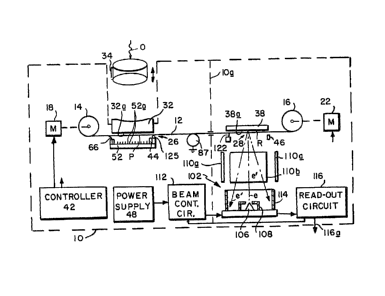
Referring to FIG. 1, the components of my system are
mounted inside a hermetically sealed housing 10 which is
maintained under a high vacuum in the order of lo-B Torr.
Suitably positioned inside the housing is a recording member
in the form of a long optoelectronic tape 12 that is
stretched between a pair of spools 14 and 16, rotatively
mounted in housing 10. These spools are rotated in either
direction by a pair of drive motors 1~ and 22, respectively,
so that selected frame areas or frames 12a (FIG. 2) along
~3~7 ~ E5-006
-28-
the tape can be positioned at a write station, shown
generally at 26, where electronic images can be written or
recorded on the tape, or at a read station, shown generally
at 28, separated from station 26 by a vertical partition
lOa, where electronic images already recorded on the tape
frames can be read or retrieved from the tape to produce
corresponding picture signals suitable for controlling an
electronic display or printer so that the stored images can
be viewed or reproduced.
In the system 10 specifically illustrated in FIG. 1,
the optical images are recorded on the tape frames 12a.
Accordingly, the system includes a transparent platen 32
mounted in a gas-tight manner in the housing 10 wall. The
platen has an inner surface 32a which positions a frame 12a
of tape 12 at a focal plane P which constitutes the exposure
position of the tape. A projector, shown generally at 34,
is adjustably mounted to the housing directly opposite
platen 32 so that an optical image O in a field of view can
be brought to focus at the focal plane P, i.e. at the tape
frame 12a in the read station 26. The platen 32 may also
constitute an optical element in the optical path to flatten
the field over the focal plane, to divide the incoming light
into its primary color components, etc. and, when a voltage
~ ?;!~ E5-006
-29-
i5 applied to attract and hold the tape flat against the
platen 32 surface.
Preferably the platen is of the type disclosed in my
above-identified application that has light-sensing
capabilities that can be used to focus projector 34
automatically prior to each exposure and to set the exposure
duration when an image is being recorded on the tape at
station 26. sy applying currents to motors 18 and 22 of the
appropriate magnitudes and polarities, tape 12 may be kept
taut and moved in either direction to position a selected
frame 12a opposite platen 32 at focal plane P. ~he
mechanism for transporting tape 12 may include other
components such as tape edge guides and a tape gate for
accurately locating each increment or frame of the tape at
an exposure position at platen 32 in focal plane P.
Another platen 38 at read station 28 has a flat surface
38a adjacent to the stretch of tape from spool 16 that
defines a scanning plane R. When the electronic image on a
particular frame is to be retrieved from the tape, the
spools 14 and 16 are rotated, via their motors 18 and 22, to
position that frame at plane R so that the frame can be
processed in a manner to be described later.
~ 3 ~ E5-006
-30-
The servo motors 18 and 22 that rotate spools 14 and 16
receive drive signals from a controller 42 in housing 10.
The controller controls motors 18 and 22 to position a
selected tape frame 12a at either focal plane P or scanning
plane R by counting tape position signals from a pair of
optical detectors 44 and 46 mounted opposite platen surfaces
32a and 38a, respectively. These detectors respond to tape
frame position marks 92 printed on an edge margin of tape 12
as shown in FIG. 2. Detector 44 emits a signal to
controller 42 when a tape frame is positioned properly for
imaging at focal plane P. A similar signal to the
controller from detector 46 indicates that a frame is
properly positioned for readout at scanning plane R. The
electrical power for motors 18 and 22 and controller 42 and
the other electromechanical parts of the system derives from
an appropriate power supply 48 mounted inside housing 10.
Still referring to FIG. l, also located at write
station 26 is a field emission device or electron source 52
which is positioned opposite platen 32 so that it overlies
the tape frame present at focal plane P. During the
exposure process when an image is being written on the tape,
source 52 is activated by controller 42 so that it directs a
cloud of electrons from its discharge points ~2a against the
~ ~- 3
E5-006
-31-
undersurface of the tape frame present at focal plane P. As
we shall see, the undersurface of the tape frame at plane P
becomes charged with these negative carriers, enabling that
frame to acquire and store an electronic image corresponding
to the optical image projected onto that frame by projector
34. The amount of the charge is controlled in terms of time
and magnitude to assure the capture of the maximum amount of
information contained in the image to be recorded. The
electron source 52 may also be used to eliminate an electric
bias field (if one is present) from each tape frame after
exposure of that frame by removing excess charge carriers
from the frame.
Referring now to FIGS. 2 and 3 which show the
optoelectronic tape 12 in greater detail. Preferably the
tape is of the type disclosed in detail in my above
application which disclosure is incorporated by reference
herein. Therefore, the tape description here will be
somewhat abbreviated. The tape includes a flexible,
optically clear, ribbon-like monocrystalline sapphire (Al2O
base or substrate 56. Added to that base are a thin
modulator 58 composed of a photoconductive material such as
silicon (Si) or gallium arsenide (GaAs) and a very thin,
i.e. 1000 Angstroms dual-material storage layer 62. A very
~ Q,i~r,,s 7' ' E5-006
-32-
thin boron or phosphorous-doped zone 58a of modulator 58
(i.e. n-doped with fixed positive charges) is present
adjacent to base 56 to serve as an electrode. The remaining
zone 58b of modulator 58 is free of additives.
The dual-material storage layer 62 is composed of a
very thin (about 1000 Angstoms) storage zone or layer 62a
composed of a suitable dielectric material such as silicon
nitride (Si3N4) and an ultra-thin ti.e. about 30 Angstroms)
interfacial zone 62b of an anisotropically acting dielectric
material such as silicon dioxide (SiO2) at the underside of
zone 62a. Zone 62b exhibits electrical insulating behavior
that prevents penetration of thermally generated or even
photogenerated charge carriers in modulator 58 to the
undersurface of storage zone 62a; zone 62b does allow
tunneling through to the storage zone 62a of photogenerated
charge carriers under the influence of a suitable
superimposed strong orthogonal electric field through the
tape zones 58a and 58b, 62b and 62a. In other words, charge
carriers from modulator 58 that have tunneled through zone
62b under the influence of an applied field are "pinned" to
the underside 62c of storage zone 62a in so-called charge
centroids. In the absence of that field, zone 62b prevents
additional charge carriers from reaching the storage zone
~ g ~
33 64421-410
and disturbing the properly accumulated charge count there. Thus
zone 62b traps in storage zone 62a a]] photogenerated positive
charge carriers created during the exposure step, thereby storing
electronic signal patterns spatially in that zone of the tape and
preventing also any lateral movements of said charge carriers in
zone 62a so that an lmage having exceptional resolution can be
maintained on tape 12.
Tape 12 may be made, for example, hy the process described in
my copending Canadian application Serial No. 539,271, filed
June 10, 1987. The tape has extremely high sensitivity or
photospeed and has the capacity to acquire a very high-quality
electronic image corresponding to the optical image projected onto
it at write station 26 by projector 34. Because of the barrier
and trapping functions of the tape's unique dual-material storage
layer 62, an image can be stored on the tape for several years
without any appreciable degradation of that image.
During a write operation, the frame area positioned at focal
plane P is imaged by projector 34 and simultaneously charged by
electron source 52. proper exposure of the tape requires that
voltages from power supply 48 be applied to the tape's conductive
zone 58a. Accordingly, in the tape
~ S~; E5-006
-34-
edge margin, the material zones 62a, 62_, and 58b are etched
away so that a conductive strip 64 can be laid down on
conductive zone 58a. Preferably, the strip 64 adjacent to
each frame 12a may be isolated electrically from the similar
strips associated with the other frames of tape 12 so that
electrical connections may be made to each frame
independently. As shown in FIGS. 2 and 3, when a particular
frame 12a is present at focal plane P, a wiper contact 66
mounted to source 52 contacts strip 64. As shown in FIG. 3,
contact 66 is connected to switch 72 in the system's
controller 42. Alternatively, electrical connections to the
strip may be made through spool 14 or 16.
~ eferring to FIG. 2, to enable my system to record
color images, the light from projector 34 is passed through
an array of numerous, thin, parallel, transparent, abutting,
band width-limited, electrical insulating color filter
stripes 76 applied to the platen surface 32a that supports
tape 12 at focal plane P. In some applications, the filter
stripes may be on the front face of the tape itself. It is
generally desirable to make filter stripes 76 wavy instead
of straight~ as shown. This avoids periodicity problems
that could occur if the object being focused upon by
projector 34 is composed of alternate light and dark bands
~ ~ ~ r~ ' E 5 - 0 0 6
-35-
extending parallel to straight stripes 76 (e.g. a picket
fence). Although the drawing figures illustrate stripes 76
as being relatively wide and few in number, in actuality,
there may be several thousand stripes in the array on 21aten
32, each stripe being in the order of only a few (e.g. 2.5)
microns wide. The filter stripes 76 on platen 32, while
they may be a diffraction filter, actually consist of very
fine abutting parallel red (R) green (G) and blue (B) films
which divide the incoming light image into its color
components thus, when a tape frame 12a is exposed at plane
P, the image applied to the image area I of the frame
consists of red, green, and blue color components of the
picture projected onto the frame, which components are
interlaced on the frame. In other words, the picture
information for each color component of the picture is
stored every third line of the tape frame at plane P. A5
will be seen, the color filter stripes coincide with the
raster path of an electron beam that scans the frame in
order to read out the image thereon when the frame is
located at read station 28.
The system may also include provision for
automatically focussing projector 34 prior to writing an
image on the tape and for controlling the charging of the
~ 6 i ~; E5-006
-36-
tape by electron source 52 during the exposure process.
Since those provisions are described in my first-mentioned
application, they will not be detailed here since they are
not really part of the present invention.
Refer now to FIG. 4 which shows the electrical
environment of tape frame 12a durinq exposure and to FIG. 5
which depicts a typical characteristic curve C for the tape
frame being expos~d. Effectively, controller 42 controls a
variable resister 82 connected in series with electron
source 52, a 5-100 volt tap of power supply 48, switch 72,
and tape frame 12a at zone 58a thereof so that the darkest
part of the light image being projected onto frame 12a
receives a selected minimum exposure, i.e. at least 109
photons/cm2, corresponding to 10-3 ergs/cm2. In a typical
case, the charging current in the FIG. 4 circuit is under
one ampere and persists for 1 microsecond to 1 second (or
more), depending upon the amount of light incident on the
tape. Each incident photon produces one electron-hole pair
in modulator 58 as shown in FIG. 4. In the portions of
modulator 58 where the light image is darkest, the incident
light emanating from a faint image typically produce in the
order of 30 x 103 electrons/cm2. For the brightest parts of
the modulator, there may be in the order of 30 xlOll
.
-
E5-006
-37-
photogenerated electrons/cm2. Thus, the charqes stored at
different locations on tape layer 62 may vary from, say, 20
electrons/resolution element to 20,000 electrons/resolution
element, permitting the retrieval of far more that the
desired 32 different gray level steps G in the image being
recorded on frame 12a, as shown in FIG. S.
The electric field across the tape causes the
photogenerated electrons to move toward conductive zone 58a
from where they are conducted away to ground via contact 66.
The photogenerated positive carriers or holes move toward
tape storage layer 62. Under the influence of the strong
superimposed external bias field e~tending between electrode
zone 58a and the virtual electrode formed by electron
deposition on surface 62d of layer 62 and of the additional
internal fields formed between negative electronic charges
on that surface and the innate positive potential of the
holes, these positive charges tunnel through the interfacial
zone 62b and are trapped in the undersurface 62c of the
dielectric zone 62a to a depth in the order of 100 Angstroms
in numbers that are in direct proportion to the image
brightness in the different parts of the image area I of the
frame 12a. These positive charges are balanced by equal
numbers of electrons from source S2 that repose on the
~ ~P~ E5-006
-38-
surface 62d of layer 62 as shown in FIG. 4. Although the
charge domains or numbers of electrons stored at adjacent
resolution elements on tape surface 62d may vary to
establish the contrast or gray levels in the stored
electronic images, the potential verses electrical ground,
i.e. zone 58a, is equalized throughout the frame. Thus,
during exposure, control section 42 charges frame 12a to a
voltage and for a time so as to operate on the optimum
segment of the tape's characteristic curve C shown in FIG.
5, under the prevailing lighting conditions.
Thus during the exposure process, electron source 52,
under the control of controller 42, disperses a specific
amount of negative charges to tape surface 62d during the
exposure duration to equal the maximum number of
photogenerated charges which have tunneled through tape zone
62b, thereby establishing a charge equilibrium in the
storage zone 62a. Accordingly, a perfectly exposed,
electronic equivalent image, corresponding to the photonic
image projected onto focal plane P, is acquired by tape
frame 12a and stored in its storage layer 62. As shown in
FIG. 4, the electronic images are present on layer 62 as a
topographical distribution of different-charge coulombic
domains over the image area I of the tape frame 12a. This
~ 3 ~ 7 ..; E5-006
-39-
distribution is composed of two parts, namely the charges
which were deposited on layer 62 at the beginning of the
exposure step to establish the initial internal bias field
between the surface 62d of layer 62 and the electrode zone
58a, plus the photogenerated equivalent charges created by
exposure of the tape frame.
Thus, the number of electrons at each point on the
surface 62d equals the number deposited initially (circled
in FIG. 4) plus a number of electrons corresponding to the
number of photogenerated positive charge carriers that
tunneled through zone 62b during the exposure step
(uncircled in FIG. 4). In the normal mode of operation, the
initial charge (circled in FIG. 4) remains on tape frame 12a
after the exposure step is completed, i.e. after electron
source 52 is shut off and switch 72 is opened. On the
imaged frame 12a, then, the charges on zone 62a are
spacially varied by the number of photogenerated carriers
which became superimposed on the blanket of evenly
distributed carriers present in thermal equilibrium
initially. Thus, for a typical photographic scene, the
numbers of opposed positive and negative charges are
substantially equal within said resolution element, but
different with respect to other resolution elements.
~ J~ E5-006
-40-
After the exposure step, when source 52 is turned off
and switch 72 is opened thereby removing the negative bias
that was set to control electron cloud current density and
duration, the positive charges which tunneled through tape
zone 62b remain pinned in place in æone 62a. It should be
noted that any free thermally generated or even
photo~enerated positive carriers now have insufficient
energy to tunnel through the zone 62b barrier and upset the
stored charge count at the underside 62c of zone 62a.
In special cases, such as low light level exposure, it
may be desirable to eliminate the electrical bias field
applied to the tape frame 12a through the removal of the
charges deposited initially on the frame. This passivation
step, if used, involves the operation of the electron source
52 in circuit with the tape so that each primary electron
from source 52 results in the emission of more than one
secondary electron from the surface 62d of tape layer 62.
This emission gradually turns that surface electrically
neutral or positive with respect to electrode layer 58a.
Referring now to FIGS. 3 and 4, the bias removal of frame
12a is initiated automatically by controller 42 immediately
following the exposure step while frame 12a is still at the
write station 26 in the darkness of compartment 10.
~ '; E5-006
-41-
Controller 42 closes a switch 86 momentarily (e.g. for 1/10
microsecond) so that a negative voltage in the order of 500V
from power supply 48 is applied to the strip 64 and
electrode layer 58a of that frame by way of contact 66 on
source 52. Simultaneously, the controller turns on electron
source 52, Ctill overlying that frame, which directs a flood
of energetic electrons to the surface 62d of storage zone
62a causing the emission of secondary electrons from that
surface, in numbers that exceed the number of arriving
primary electrons from source 52. Once the electrons are
removed from the darkest parts of the image areas (i.e.,
those electrons deposited initially at the beginning of the
exposure step, circled in FIG. 4), only the uncircled
electrons remain which counterbalance the positive charges
pinned to the underside of zone 62a. Thus, only the ch~rges
corresponding to the image will remain on the frame. In
response to incident light varying from 6X10B photons/cm2 to
6X101l photons/cm2, a typical electronic image might vary
from 20 electrons/pixel to 20,000 electrons/pixel,
corresponding to a field strength of 70 V/cm to 70x103 V/cm
inside the storage zone 62a. The removal of the blanket
surface charge from surface 62d over the entire area leaves
the stored image completely free of this blanket bias
~ ; E5-006
-42-
charge. The surface charge in the exposed portions of the
frame now reflects only the image information.
Instead of using source 52 for the passivation step
just described, in some applications, it may be preferable
to position a separate electron source (not shown) for that
purpose in housing 10 between the write station and the read
station. Then when a tape frame is moved to the latter
station, the emitter needles of that source rake the
undersurface 62d of the tape to remove the bias charge
therefrom as just described.
Still another way to remove that bias charge is to
provide an electrically grounded conductive roller 87
between the two stations, as shown in FIG. 1, so that the
roller touches the tape surface 62d as the tape is ad~anced
to station 28. It should be noted that those electrons
bound to underlying positive charges in zone 62a and
representing the stored image remain unaffected as the
roller 8~ rolls over tape frame 12a.
The magnitude of the dark current in light modulator
layer 58 during exposure and bias removal is temperature
dependent and relatively small in comparison to the charges
created during exposure. However, if temperature
compensation is desired, a temperature sensor (not shown)
~ E5-006
-43-
may be mounted in housing 10 and coupled to controller 42 so
that the duration of the exposure and bias removal steps may
be varied to compensate for those temperature changes.
Referring now to FIGS. 2 and 3, simultaneous with the
recording of the image on each tape frame 12a as just
described, an electronic fiducial mark 92 is recorded in an
edge margin of that frame area outside the image area I
thereof as shown in Fig. 2. As will be seen later, these
marks 92, recorded at the same times as the images, enable
the system, prior to each read-out operation, to set the
initial or home position and skew of the electron beam that
scans the tape during a read operation at station 2~ to
compensate for any slight mispositioninq of each tape frame
12a at its position at the scanning plane R when an image is
read from the frame, with respect to its position at focal
plane P when that same image was recorded on that frame.
My system records these marks 92 on the tape by means
of a light unit 94 located in platen 32 at the upper
righthand corner thereof at focal plane P. As shown in FI~.
2, unit 94 comprises an elongated light source 94a such as a
LED or a laser diode extending parallel to tape 12 and which
preferrable emits green (e.g. 500 nm light). The other
component of unit 94 is an opaque mask 94b positioned at
~ J ' J E 5 - ~ 0 6
-44-
platen surface 32a to be in intimate contact with frame 12a
at focal plane P. The mask has a precise narrow slit 96a
extending parallel to the tape (i.e. X axis) with a (Y axis)
cross-slit 96b positioned adjacent to the foward edge of
platen 32. Each time an optical image is recorded on the
image area I of a tape frame 12a, controller 42 energizes
light source 94a so that the marginal area of tape frame 12a
opposite slits 96a and 96b receives a saturating dose of
light. Resultantlyr an easily detectable electronic
fiducial mark 92, having cross arms 92a and 92b, is recorded
on tape 12. As shown in FIG. 4, the fiducial mark actually
consists of a large number of negative charges deposited on
surface 62d of frame 12a outside its image area I ~with an
equal number of underlying positive charges in tape zone
62a).
After an electronic image is recorded on a tape frame
12a as just described, that image can be read out or
retrieved from the tape by positioning that tape frame in
the scanning plane R at read station 28 by appropriately
driving spool motors 18 and 22 via controller 42. As
mentioned previously, controller 42 counts pulses from tape
position detector 46 so that it "knows" when a particular
-
, r~ ~
ci..l ~ ul ~! J E5-006
-45-
frame along the tape, say frame number three, is properly
positioned at plane R for read-out.
As seen in FIG. 1, located opposite to the read station
28 of my system is an electron gun shown generally at 102.
The gun includes an electron emitter or cathode 106 that
produces a stream of electrons e. An accelerating anode 108
accelerates the electrons toward the surface 62d of the
frame 12a at scanning plane R so that the beam which
impinges on the tape is finely focused to a diameter that
is slightly less than the width of the filter stripes 76
(FIG. 2). Gun 102 also includes the usual horizontal and
vertical deflection plates llOa and llOb. The fields
developed between these plates are controlled by a beam
deflection control circuit 112 in housing 10 so that the
electron beam sweeps out a raster on the surface 62d of the
frame 12a at read plane R. As mentioned previously with
respect to FIG. 2, the lines L of the raster should
correspond to the lines on frame area 12a that were recorded
through the array of filter stripes 76. When lines L are
sinusoidal or wavy to avoid the "picket fence" effect
described above, circuit 112 is arranged to drive the beam
along a corresponding wavy path as it sweeps across the
frame surface.
:~ d r ~ ~
~ , E5-006
-46-
As shown in FIG. 2 and as will be described in more
detail presently, the impingement of the beam electrons e on
the tape frame 12a causes secondary electrons e' to be
emitted from the tape whose numerical distribution by pixeis
or resolution elements in the scan represents the electronic
image stored on the frame. The secondary electrons e' are
collected by an electron collector 114 encircling electron
emitter 106 and a picture signal is developed which is the
electrical analog of the stored image. That signal is
applied to a read-out circuit 116 contained in housing 10
where it is amplified, digitized and otherwise conditioned
before being applied to an output terminal 114a which may be
~oupled to a video display or printer (not shown) where the
retrieved image can be viewed or reproduced.
When system 10 is to read the image on the frame 12a
present at scanning plane R, controller 42 closes a switch
118 which, as seen in FIGS. 1 to 3, connects a wiper
contact, or equivalent, thereby engaging tape strip 64 at
station 28, and thus tape zone 58a, in a high voltage (i.e.
300V) DC circuit with emitter 106 (maintained at -2KV).
Whereupon, the emitter emits a small diameter (typically 2
micrometers) electron beam which impinges the selected tape
frame 12a at scanning plane R. Since tape 12 is infrared
~ ., E5-006
-47-
sensitive, the electron beam source 106 must be a cold field
emission device rather than a thermionic device thereby
avoiding exposing the tape to infrared radiation while it
is being read. Cold cathode emission sources of this type
have, to our knowledge, not been used previously in such a
scanner application; they can be operated with very little
power (about 1 nanoampere).
Where the beam e impinges the frame 12a, secondary
electrons e' are emitted from tape zone 62a at that point.
As noted previously and as shown in FIG. 4, the charges on
zone 62a consist of the photogenerated positive charges
pinned to the underside of zone 62a and an equal number of
negative signal charges or electrons resident on zone
surface 62d (uncircled in FIG. 4) and, if not removed as
described above, bias electrons (circled in FIG. 4) present
as a result of the initial bias field applied to the tape
during the exposure process described above. The surface
electrons on zone 62a are bound in equal numbers to positive
charges, with excess electrons resulting from the initial
bias field being less strongly bound to the surface so that
they can be removed easily via a short circuit with the tape
electrode layer. The underlying positive charge carriers at
the underside of zone 62a remain pinned at the their
~ 3 ~ ~ J ~ ~, E5-006
-48-
locations, as are their corresponding negative charges on
surface 62d.
The waveform S in FIG. 6 shows the variation of the
secondary electron emission ratio (R~ with primary electron
energy, i.e. no. of primary electrons/no. of secondary
electrons versus primary beam voltage when the beam from gun
102 strikes tape 12. The ratio R is unity at two locations
on waveform S, namely at a first voltage Vc~ and a second
voltage Vc2. At these two crossover potentials, the number
of secondary electrons ejected from tape zone 62a at each
pixel equals the number of primary electrons e in the beam
from source 106 that impinge that pixel. The present system
normally operates between the first and the second crossover
point Vc2 and near the latter so that the primary electrons
have sufficient energy to partially penetrate the layer 62,
but not deep enough to reach the positive charges pinned to
the underside of that zone. Consequently, the electron beam
which scans the tape frame in order to read the image
therefrom does not affect the image-representing positive
charge pattern at the underside of frame 62a so that the
integrity of the negative charge domains on surfae 62d is
maintained.
~ E5-006
^ ~ l ~ i, ~
-49-
The impingement of primary electrons e on tape frame
12a results in the emission of secondary electrons from
within the bulk just beneath the surface 62d of layer 62
with said secondary electrons being created throuyh electron
collisions within the bulk of the layer 62. These newly
generated negative charges form the electron flux e' whose
intensity is determined by both the coefficient of secondary
emission (ratio) and the influence of the internal fields
which make up the image-wise charge domains, with the latter
being able to restrict the number of secondary electrons
which are emitted. All of the electrons in the secondary
electron flux e' are collected by collector 114 which
thereupon produces an output signal reflecting the electron
count. It is apparent, therefore, that the number of
electrons, i.e. flux e', detected at each plcture element
point in the primary beam scan (and hence the amplified
collector output signal) will depend upon the field
intensity present at said pixel which modulates the number
of actually emitted secondary electrons. More particularly,
where the number of stored electronic charges on zone 62a is
smaller, corresponding to a point outside image area I or to
relatively dark or unexposed point inside area I, the number
of electrons in the secondary flux e' will be larger. The
~ 3 ~ ; E5-006
--50--
maximum return flux occurs in the areas where no fields are
present. There will likewise be a decrease in the number of
secondary flux electrons from a point on the swept frame
area where the number of stored charges on zone 62a is
larger. At the fiducial mark 92 the secondary flux is
mimimal because the internal field is at a maximum. Thus by
subtracting from the electron count detected by collector
114 the electron contribution due to secondary electron
emission and blanket charge electrons (if present), the flux
electron count produces an output signal from the
collector/amplifier which represents the electronic charge
distribution on tape frame 12a which, in turn, corresponds
exactly to the optical image recorded on that frame at write
station 26.
Read-out by secondary electron emission detection in
this fashion allows the integration of the collector with a
channeltron or dynode type amplifier. These are known
electronic devices which require low power, yet produce a
current output which is as much as l,000,000 times stronger
than the input represented by return flux e', while
introducing mimimal electrical noise. Resultantly, for each
scan of a tape frame 12a at read station 28, my system will
provide a highly amplified signal representing first thP
r~
S : E 5 - 0 0 6
--51--
electronic fiducial mark 92 recorded in the margin of that
frame to zero-set the scan beam electronics and then the
electronic image stored in that tape frame~s image area I.
Thus the read-out process carried out by the system
involving the field modulated count of secondary electrons
emitted from tape 12 is totally different from the prior
scanning methods described at the outset which detect a
capacitively modulated field unrelated ground current signal
from a recording mediumas the reading beam establishes
charge equilibrium and destroys the signal. Here, by
detecting and simply counting individual electrons in a
secondary flux e' modulated by the topographic field
intensity distribution on tape surface 62d, rather than by
detecting current flow through the frame, the system can
take advantage of the highly sensitive, defect-free nature
of the tape 12 to produce a picture signal which contains
minimal noise and has extremely high resolution combined
with an exceptional greyscale. Furthermore, it can
accomplish this at a lower read-out or scanning voltage than
those prior systems, thereby conserving power. In addition,
the read-out is non-destructive with regard to the field
domains in layer 62 and, for this reason alone, is superior
to other techniques.
E5-006
' s,~, ..
-52-
The beam from gun 102 typically scans 16,000,000 ~,G,s
resolution elements in nine seconds or 5,300,000 monochrome
resolution elements in three seconds, corresponding to a
dwell time at each raster resolution element or pixel on
frame 12a of about 0.6 microseconds. A typical FIG. 1
system which is designed to detect 20 to 20,000 electrons
during the dwell time at each resolution element (i.e.
1:1000 dynamic range) would require a minimum beam current
in the beam from gun 102 of 5x10⁻⁹ amp or 5 nanoamperes.
Using a collector such as the first stage of a low-noise
electron multiplier (channeltron/dynode), the signal current
(i~), noise current (in) and output signal current (i6n) may
be determined. Thus, for a low light level in which the
minimum light signal is represented by 20 electrons per
pixel and the maximum by 400 charges per pixel, the beam
current must be equal or greater than the maximum number of
charges per pixel; with this constraint, the noise
associated with the flux of 400 primary electrons in the
elected scan time of 0.6x10⁻⁶ sec. per pixel is as follows:
scan time per pixel = 0.6x10⁻⁶ sec
Maximum beam current (ib) = 400x16.61xolcO
= 10-1 amp./pixel
E5-006
-53-
After amplification, the current iSn = 10lx106
= 10-4 amp./pixel
The noise current associated with the beam current is
i" = ( 2eibf ) ~
where e = 1.6xl o~l9 coul.
f = 1/(2x0.6xl- ) s~c
= s.4x10-12 amp.
Therefore, the signal-to-noise ratio
i /i = (400)~ = 10.7xlO 12 = 20:1
If that ratio were reduced to a minimum usable level of
5:1, the corresponding number X of electrons would be
5/1 = X e/scan time = (X)l/2
(X)1~2 e/scan time
X = 25
The dynamic range is therefore 400/25 = 16:1 of target
electrons.
The output signal current from the target (before being
applied to the electron multiplier) ranges from a minimum of
? `'~
E5-006
-5g-
i ~ 25 elec x 1.6xlO-19 coul. x
sn pixel electron 0.6x10⁻⁶ sec./pixel
isn = 6.67 x 10⁻¹² amp.
to a maximum of
i = 400 x 1.6xlO-l9
sn 0.6 x 10
= 10.7 x 10⁻¹¹ amp.
In a preferred embodiment of my system, means are
provided to vary or select the primary beam current
commensurate with the maximum exposure which an image frame
saw in the field of view. For this purpose, the particular
frame (as is each frame on the tape) is marked with an
electronic code whose value indicates the amount of light
which the exposure meter reads prior to the exposure for
said frame, as the meter sends the exposure control signal
to the electron cloud qenerator 52.
Thus, for example, if the exposure equalled 10~l erg/cm2
then the light flux per pixel produced 20,000 electron-hole
pairs, which means that the primary beam should be set at
20,000 electrons minimum during the pixel scan time. If the
exposure were 10-3 erg/cm2, then the beam would be set to 20
electrons/pixel during the scan time in order to detect the
full equivalent signal which the 20 electron-hole pairs
produced during the exposure.
~r~ E5-006
-55-
For the maximum detectable exposure,
Noise current = 3.77 x 10ll amp.
Signal-to-noise ratio = 141:1.
For a signal-to-noise ratio of 5:1, the corresponding
number of electrons ~ 25.
Dynamic range equals approximately 800:1 of target
electrons.
Output signal current iSn = 6.67 x 10-l2 amp. min. to
5.33 x lO-9 amp. max.
It will be apparent that the system could also be
arranged to have several current steps during the dwell time
of the beam in each pixel or resolution element of the scan
~aster. For example, the beam current might be stepped up
to 10 4 amp to provide another dynamic range level of
160,000 to 256 x 10~ electrons. Normally, however, this
enormous range is not required because a typical scene
contains only about 100:1 contrast between the light and
dark areas thereof.
In some applications, the scan control circuit 112 can
be arranged to control the beam e from gun 102 so that it
scans two different rasters. A rough scan, say every other
or every third line L, may be executed (for each color) to
E 5 - O 0 6
- 5 6 - ~ 3 ~
provide picture signals suitable for previewing on a video
display to which the present system may be connected to see
if the correct image is being retrieved. ~hen, if the image
is correct, a regular scan at the final resolution ~ay be
performed to reproduce a hard copy of that image in a
printer connected to the system at terminal 116a.
Also, if the electronic images were recorded on tape 12
in the presence of an electrical bias field caused by the
deposition of a uniform blanket layer of electrons on the
tape surface 62d, these bias electrons (circled in FIG. 4),
unless removed after the exposure step as described above,
are still present on tape surface 62d at the recording
station 28. In my system as described thus far, the
electron source 106 is preferably operated between the
second and third crossover points shown in FIG. 6, so that,
as noted above, the number of electrons in the secondary
electron flux e' from points in unimaged areas of the tape
e~uals the number of ejected secondary electrons minus the
number of image-wise electrons which were prevented from
leaving the material due to the internal fields. As noted
above, during the scanning process, there are enough
secondary electrons ejected from the tape to drive each
point on the tape surface sufficiently electropositive to
E5-006
_57~ 7~ :~
offset the negative bias charge present at that location on
the tape. In this event, as shown in FIG. 7, there will be
left behind only the negative signal charges at the surface
62d which are more strongly bound to the underlying image-
representing positive charges pinned at the underside of
zone 62a.
When my system scans a frame 12a during read-out,
unlike prior systems described at the outset, it does not
destroy the electronic image stored on that frame. On the
contrary, the system refreshes that imaqe which can be read
over and over again. This is because durinq scanning, which
takes place in the darkness of housinq 10, there are no
photo-induced electron-hole pairs produced in the tape's
modulator 58. Nor is there any buildup of charqe on the
tape's storaqe layer 62 because, as noted above, the
positions of the positive charqe carriers pinned at the
underside of zone 62a remain undisturbed by the beam, while
the negative image-wise charges at surface 62d are
replenished. This may be accomplished by exposing the tape
frame to electrons from source 52 prior to readout or by
operating electron qun 102 at a lower enerqy level and
scanninq the frame prior to readout so that electrons
impinge the tape without causing secondary electron emission
E5-006
-58- ~ ~ r~ '~3 ''~
therefrom. Thus a charge balance is maintained across layer
62 at each point thereon, as depicted in FIG. 7. As a
consequence, the field strengths of the charge domains
distributed on layer 62 of each frame 12a are maintained,
allowing theoretically infinitely repeated read-outs of that
frame.
In fact, due to the high degree of perfection of tape
12, the electronic images recorded on tape 12 will remain
there for several years unless they are erased
intentionally. In my system, such erasure is accomplished
simply by positioning the frame 12a containing the image to
be erased at write station 26 (or elsewhere in housing 10)
and energizing a U.V. lamp 125 mounted to source 52. The
short wavelength radiation from that lamp renders the tape
layer 62 conductive thereby removing the image-representing
charge pattern from that frame.
As mentioned previously, the strong electronic
fiducial mark 92 recorded on each frame 12a is used to
initialize the beam scan prior to reading the image stored
on that frame. More particularly, at the outset of each
read-out operation, controller 42 causes beam control
circuit 112 to execute a search routine in order to "find"
fiducial mark 92. According to this routine, circuit 112
r~ ~ i'`! ' ' E 5- 0 0 6
--5g--
deflects the primary beam e so that it sweeps out a spiral
or circular motion (or other suitable geometric sweep
pattern) while advancing along the upper margin of the tape
where the fiducial mark 92 is located, i.e. the region
between the edge of frame 12a and the edge of image area I.
When the beam in its rotary motion passes through an arm 92a
or 92b of the fiducial mark, there results a sharply reduced
burst of electrons in return flux e'. The few electrons in
the signal are caused by the retardation of secondary
electron emission due to the strong electric field in the
fiducial mark area. These few fiducial mark electrons
(voids) are collected by collector 114 and detected as such
by threshold detection in read-out circuit 116 which
thereupon issues a control signal to control circuit 112.
In response to that signal, circuit 112 causes the primary
beam circular sweep to cease translating along the tape
margin and to scan in the nearby area until the collector
detects four electron voids signifying that beam e is
sweeping across the two fiducial mark cross-arms 92a and
92b. The presence of these four signals at the output of
collector 114 indicates that beam e is more or less centered
on the fiducial mark 92. These signals are applied ~o
circuit 112 to cause that circuit to shift the beam slightly
E5-006
-60-
in one direction or another until the signals are equally
spaced apart in time signifying that the axis of beam e is
aligned with the fiducial mark axis and that the X and Y
deflection axes of the beam are parallel to the fiducial
mark arms 92a and 92b respectively.
If desired, the cicuit 112 initialization routine can
be arranged to cause beam e to execute several circular
scans of the fidicual mark 92 to provide redundancy and thus
assure the accuracy of the "home" position setting of the
beam. At the end of the initialization routine, the now-
ascertained position of the fiducial mark 92 on the X and Y
scan coordinates is stored in a memory in circuit 112 and
the actual read-out scan is started at a fixed offset from
that point, e.g. at the corner of image area I.
The significance of initializing the electron beam
prior to reading images from the tape relates to the fact
that the very fine signal pattern stored on each frame 12a
was recorded contemporaneously with the electronic fiducial
mark 92 on that frame, thus linking the 2.5 micron-wide
color sripes 76 to the scan coordinates and deflection
electronics in cicuit 112 which must guide the 2.0 micron
diameter beam e during read-out. ~y recording the fiducial
mark 92 and the image on frame 12a simultaneously while the
f~ ~ ~
E5-006
-61-
tape, and hence that frame, was stationary and frozen
geometrically at exposure station 26 and prior to any, even
very minute, movement of the tape away from the filter
stripes 76 assures that the beam e will sweep along raster
lines L that correspond exactly to the lines on frame 12a
that were exposed through the filter stripes. searing in
mind that the lines of color information on frame 12a are in
the form of electrical signals only (i.e. charges), they
carry no identification of their optical coloration.
Accordingly, the providing of fiducial mark 92 and the
initializing routine described above assures that during a
read operation the beam e is following or sweeping out the
correct raster path on frame 12a even though that frame
might have been shifted or skewed to some extent so as to
place the equivalent color stripe information in a shifted
position with respect to the electron source 106.
After the beam has been "zero-set" ready for image
scanning, it first will seek out an exposure code area in
which the exposure meter left a recorded exposure value
which now can be used to set the beam current commensurate
with the electron charge density values which represent the
image over the frame as described previously.
E5-006
-62-
Referring now to FIGS. 9 and 10, instead of reading the
electronic image stored on tape frame 12a by electron beam
scanning, the tape can also be read by detecting so-called
"tunnel electrons" emissions. For this purpose one
preferably uses a linear array of very sharp tungsten
sensing needles 132 which move across the tape surface in
rake-like fashion 62d as shown in FIG. 9. This read-out
technique uses the tunnelling electron phenomenon described,
for example, in the publication Scientific American, August
1985 Edition, pages 50 to 56. As disclosed there, due to
their wave-like nature, electrons on a surface leak out and
form a cloud above that surface. Therefore, as best seen in
FIG. 10, when a needle tip 132a is spaced sufficiently close
to the charged tape surface 62d, electron clouds Cl and C2
present above those surfaces gentley touch. When a voltage
is applied between the tip 132a and the tape's electrode
layer 58a, so-called tunnel electrons flow from the tape
surface to the needle tip along a narrow channel T through
these overlapping electron clouds, giving rise to a
tunnelling current it.
Since the density of an electron cloud C~ or C2 falls
expotentially with distance, the tunnelling current it is
very sensitive to the distance between each needle tip 132a
) r~
~ E5-006
-63-
and the tape surface 62d. A change in that distance by as
little as one atomic diameter causes a change in tunnelling
current by a factor of as much as 1000. In the FIG. 9
system, each needle 132 in the linear array is held by a
suitable needle positioner 134 and swept in a raster across
tape surface 62d by an appropriate sweep mechanism 136 such
as the one described in the above article. Each needle, in
effect, picks off electrons from the tape surface at each
point in the scan giving rise to a tunnelling current it in
needle 132. This current signal is applied to a feedback
circuit 13~ which controls the needle positioner to maintain
the needle tip 132a at a constant height above the surface
62d atoms. In this way, the scanning needle tip 132a
follows the contours of surface 62d as shown in FIG. lO.
When that distance is kept constant, the tunnelling current
it at each point or resolution element in the needle scan
depends upon the electronic structure of the tape surface
62d and the number of electrons present on that surface at
that location. ~hat current signal is also applied to an
amplifier 140 by way of a threshold circuit 142 which
subtracts the signal contribution due to tape surface
structure (i.e. the signal present in an unimaged area of
the tape). Resultantly, the amplifier output is a picture
ES-006
-64-
signal which is an exact representation of the electronic
signal pattern stored on the tape frame 12a along the line
scanned by the needle. That signal will, of course, include
the initial bias charge unless that charge is removed
following exposure as described above.
It will thus be seen that the objects set forth above,
among those made apparent from the preceding description,
are efficiently attained. Also, certain changes may be
made in the method described above and in the construction
shown herein without departing from the scope of the
invention. Therefore, it is intended that all matter
contained in the above description or shown in the
accompanying drawings be interpreted as illustrative and not
in a limiting sense.
It is also to be understood that the fo~lowing claims
are intended to cover all of the generic and specific
features of the invention herein described.