Note: Descriptions are shown in the official language in which they were submitted.
~ ~1 7857
HOMOEPITAXIAL GROWTH OF ALPHA-SiC THIN FILMS AND
SEMICONDUCTOR DEVICES FABRICATED THEREON
Field of the Invention
The invention relates to the growth of Alpha-SiC
thin films. More particularly, the invention relates to
high purity, low defect, device quality monocrystalline
Alpha-SiC thin films which are epitaxially grown via che-
mical vapor deposition on Alpha-SiC [0001] substrates pre-
pared "off axis."
Background
Silicon carbide is considered a superior
candidate material for high temperature, high power and
high frequency electronic devices due to its high melting
point, relatively large energy bandgap, high saturated
electron drift velocity, breakdown field, hlgh thermal
conductivity and chemical resistance. Its large energy
bandgap also makes it an excellent material for the blue
light-emitting diodes and radiation intensive environ-
ments.
Silicon carbide exists in hexagonal, rhombohedral
and cubic crystal structures. Generally, the cubic, zinc
blende form is referred to as "Beta-SiC" whereas the
; numerous polytypes of the hexagonal and rhombohedral forms
1 31 7857
are collectively referred to as "Alpha-SiC." The most
common Alpha form is 6H SiC.
Beta-SiC is usually considered more deslrable
than Alpha--SiC for the aforementioned electronic
applications since its electron mobility is postulated to
be higher than that of Alpha-SiC over the temperature
range of 300 to lO00 K. Furthermore, the growth
temperatures of Beta-SiC are generally lower than those
of Alpha forms for various types of growth, for example
chemical vapor deposition (CVD)~. However, the
difficulties in the growth of high quality, low carrier
concentration Beta-SiC thin films do not allow the
electron mobility to attain these postulated values. This
is believed to be due to the defects present in Beta-SiC
films, especially those grown on Si substrates.
Dislocations, stacking faults and antiphase domain
boundaries (APBs) are generated from the Beta-SiC/Si
interface and extend from the interface to approximately
3um into the bulk film. In fact, many even propagate up
to the as-grown surface. ThiS phenomenon is caused by the
differences in the lattice parameters (~0%) and -thermal
e~pansion coefficients ~8% at 473K) between the substrate
and film. Although off-axis Si (100) substrates have been
employed to help eliminate APBs, the dislocations and
stacking faults remain. When Alpha-SiC substrates are
utilized for the growth of Beta-SiC, device quality films
have been obtained, but defects persist in the form of
double positioning boundaries (DPBs).
The growth of 6H SiC films on 6H SiC substrates
via CVD has been reported since the late 1960's. Several
researchers reported the growth of 6H SiC on 6H SiC (0001)
in the temperature range of 1500-1750C, but a mosaic
morphology was observed on the as-grown surface. Such a
mosaic structure is believed to be caused by DPBs. The
growth of 6H SiC in the temperature range of 1320-1590C
was also reported, in which case, the growth direction was
t 31 7857
perpendicular to the [0001] axis. HowevPr, growth of 6H
SiC in this direction while rapid, is quite irregular and
results in unacceptable defect levels and surface morpho-
logies.
SUMMARY OF THE INVENTION
The present invention provides novel Alpha-SiC
thin films of an extraordinary, high quality that renders
them useful in the fabrication of exceptionally good
electronic devices. The films may be grown
homoepitaxially by CVD in the form of Alpha-SiC films on off
10 axis 6H SiC substrates. One advantage of the invention is
that it permits substantial latitude in the film yrowth
conditions so that the film growth conditions may be controll~
as desired to enhance growth rate, smooth surface morphology
or other film characteristics, while in all instances
producing very high quality films. The invention is well
suited for use in conjunction with currently emerging
technologies for the seeded sublimation growth of large,
high quality Alpha-Slc single crystals, which crystals may
be sliced into wafers that serve as the substrates for
thin film CVD growth. Extensive examination of films of
the invention, and the fabrication of electronic devices
on the films, has verifled their high quality and
suitability for industrial applications.
In one aspect, the invention may be defined as a
semiconductor product in the form of a device quality
SiC film deposited on a SiC substrate wherein the
substrate is formed from Alpha-SiC and has a flat
interface surface that is inclined between an angle
greater than one degree and approximately 12 off axis
with respect to a basal plane thereof substantially
~towards one of the ~1120~ directions. The thin film
preferably is an Alpha-SiC film of the same polytype as
the substrate homoepitaxially deposited on the substrate
interface surface. In certain preferred embodiments of
the invention the polytype for the substrate and thin film
1317857
is selected as 6H SiC. The angle of off axis inclination
of the interface surface of the substrate is preferably
within the range from approximately 3 to approximately
6O being more preferred, and with an inclination of
appro~imately 3 being the most preferred. Semicon~uctor
products of the present invention consistently exhibit a
smooth surface morphology, substantially uniform thickness
and a low, device compatible defect density within the
bulk film. The film may be doped to show either p-type or
n-type conductivity at selected locations therein.
In another aspect, the present invention may be
defined as a method o~ producing a monocrystalline ~H SiC
thin film on a 6H SiC substrate by the following steps:
(i) lapping a 6H SiC substrate crystal to expose a planar
surface that is inclined more than one degree off axis
with respect to a basal plane thereof substantially
towards one of the [1120~ directions; (ii) preparing the
off axis planar surface of the substrate to be receptive
to epitaxial growth thereon; (iii) heating the substrate
crystal in a growth chamber; (iv) introducing a carrier
gas, a vaporized silicon-containing material and a
vaporized carbon-containing material into the growth
chamber while providing sufficient energy to createe
surface diffusion of silicon and carbon species at the
substrate planar surface and establish a homoepitaxial
growth of monocrystalline 6H SiC; and (v) maintaining the
carrier gas, silicon-containing material and
carbon-containing material flows and the energy levels for
a time sufficient to grow a film of desired thickness.
.
BRIEF DESCRIPTION OF THE DRAWINGS
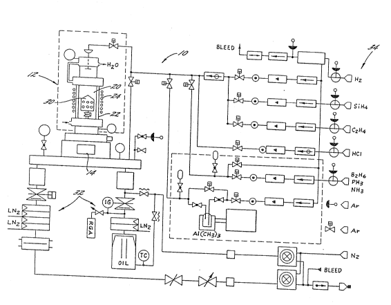
Fig. 1 is a schematic diagram of the CVD system
employed for the growth and doping of monocrystalline
Alpha-SiC thin films in accordance with the present
invention.
`1317857
Fig. 2 is a schematic diagram illustrating the
growth sequence Pmployed for the growth of monocyrstalline
Alpha-SiC thin films on "off axis" Alpha-SiC substrates in
accordance with the present invention.
Figs. 3(a) and 3(b) are optical micrograph~ of as
grown surface morphologies of films grown in ~ccordance
with the present invention. Fig. 3(a) illustrates the
surface morphology achieved by growing 6H SiC thin films
on a 6H SiC substrate inclined approximately 3O off axis
with respect to the ~OOOl)C face substantially towards one
of the {112~ directions. ~ig. 3(b) shows the surface
morphology of a film grown off axis wlth the same
inclination with respect to the (OOOl)S1 face.
Fig. 4 is an XTEM micrograph of the 6H SiC/6H SlC
interface region of the spectmen for which the surface is
illustrated in Fig. 3(a). The two TED patterns
illustrated at the leXt of Fig. 4 are from the epilayer
and substrate respectively and show identical
characteristics of [11~0] pole of 6H silicon carbide.
Fig. 5 is a plan view T~M micrograph of a film
slmilar to that illustrated ln Pig. 3(a) and Fig. ~. This
~micrograph was obtained with the electron beam parallel
to [0001~ and shows the absence of double positionlng
boundaries in the film.
Fig. 6 is a graph of carrier concentration as a
function oX depth with curve "C" corresponding to a 2 um,
unintentionally doped 6H SiC thin film of the invention.
Fig. 7 is a current-voltage charactersitic plot
of an Au Schottky dlode fabricated on a 6H SiC thin film
of the invention.
Fig. 8 is a semilogarithimic plot of
current-voltage characteristlcs o the Schottky diode
under forward bias. The ideality factor, n, is 2.15.
!
DETAILED DESCRIPTION OF THE INVENTION
While the present invention will be described `
,~...... .
1317857
more fully hereinafter with referance to the accompanying
drawings, in which aspects of the preferred manner of
practicing the present invention are shown, lt is to be
understood at the outset of the descripton which follows
that persons of skill in the appropriate arts may modify
the invention herein described while still achieving the
favorable results of this invention. Accordingly, the
description which follows is to be unclerstood as being a
broad, teaching disclosure directed to persons of skill in
the appropriate arts, and not as limiting upon the present
invention.
The present invention concerns a novel technology
that permits the growth of very high quality,
commercially useful Alpha-SiC thin films grown on
~off-axis~ Alpha-SiC substrates. In a r01ated
development, device quality Beta-SiC films have been grown
on the (0001)Si faces and (0001)C faces of Alpha-SiC
substrates, as described in Canadian application Serial
No. 581,147, filed October ~5, 1988*
entitled "Growth ot Beta-SiC Thin Films and
Semiconductor Devices Fabricated Thereon," inventors
Davis, Kong and Glass.
The Alpha-SiC substrate crystals utilized in the
examples set forth below are of three origins. First are
industrial 6H SiC crystals obtained from an Acheson
furnace. These crystals have mirror-like surfaces and are
black, indicating high impurity content. Second are 6H
SiC crystals obtained from an unseeded Lely sublimation
process. These crystals are substantially clear,
indicating relatively high purity. The third type of
crystals are 6H SiC crystals obtained from a novel seeded
sublimation techni~e recently developed at North Carolina
State University, Raleigh, North Carolina. This new
technique produces very high quality, bulk single crystals
which may be sliced into wafers, with the wafers being
used as 6H SiC substrates for the present invention.
* (corresponding to U.S. patent ~o. 4,~12,063, issued
March 27, 1990)
E3
1 3 1 7857
This sublimation process and the bulk single
crystals grown therein are describad in Canadian
Sexial No. 581,I45, filed October 25, 1988*
entitled "Sublimation of Silicon Carbide To
Produce Large Device Quality Single Crystals Of Silicon
Carbide," inv~ntors Davis, Carter and Hunter.
.
Prior to proceeding with a description of the
preparation of the substrate crystals and the CVD
processin~, a brief description of CVD system 10 will be
given, with the understanding that a more detailed
description of a substantially similar system is contained
in the cataloged doctoral thesis of Hyeong Joon Xim,
Entitled "Epitaxial Growth, Doping and Characterization of
Monocrystalline Beta Silicon Carbide Thin Films and
Fabrication of Electronic Devices," 1985, Department of
Materials Engineering, North Carolina State University,
Raleigh, North Carolina. ~-
~
CVD system 10 includes a main reactor portion 12having a loading chamber 14 which communicates with the
CVD gro~th chamber 20. The sides of growth chamber 20 are
defined by a quartz tube 22. Heat is supplied to the
growth chamber 20 by means of an RF induction coil 24.
Substrates are loaded into system 10 on a SiC-coated
graphite susceptor 30.
Pressure within growth chamber 20 is controlled
by a pressure control system which is referred to
generally by reference numeral 32. The gas supply systems
are denoted by the reference numeral 34. Systems 32 and
34, and certain other components of CVD system 10, are not
described in detail herein, but a complete description is
contained in the thesis referred to above.
Example 1
For the process described in this Example 1,
black, industrial 6H SiC (0001) wafers obtained at random
* (corresponding to U.S. Patent No. 4,866,005, issued
September 12, 1989)
1 31 7857
from an Acheson furnace were employed. Since SiC is a
polar material, (0001) wafers can terminate in either a Si
layer (0001) or a C layer (0001) and a thin crystal with
two parallel, smooth surfaces will contain one Si face and
one C face opposite to each other. However, the Acheson
derived crystals generally contain only one reasonably
flat face which is usually, but not always, Si. They
usually also contain small (1100) facets which allow the
determination of the crystal orientation.
To prepare these substrates, each was first
lapped approximately 3 off of <0001> towards one of t:wo
selected orientations using a set of beveling tools.
The first orientation is 3 towards one of the ~120~
directions. The second orientation is 3 towards one of
the ~1100} directions. (It will be appreciated that due to
the hexagonal nature of 6H SiC, each of these families of
directions refers to six directions.) Secondly, the
làpped side was mounted onto a flat plate to lap the other
side to obtain a substrate with two parallel surfaces.
The lapped wafers were then polished down
utilizing a diamond paste. Next each 6H SiC substrate was
preoxidized at 1200C in a flowing dry oxygen atmosphere
for 1.5 hour to oxidize approximately 500 A of the
polished surface in order to remove the subsurface damage
caused by the mechanical polishing.
At this stage in the process, by estimating oxide
thicknesses, the polarity of each substrate was determined
since the C face oxidizes more rapidly than the Si face.
Following this procedure, four kinds of substrates were
prepared and used. They were 6H SiC Si (0001) face and C
(0001) face 3 off towards one of the 1120~ directions
and towards one of the ~11003 directions.
Next, the oxide layer on each substrate was
removed by immersion 1Q a 49% concentration of
hydroflouric acid, followed by rinsing in deionized water.
1317857
The substrate crystal which has been prepared for
epitaxial growth thereon, preferably by the oxidation and
etching steps discussed above, is placed on the SiC-coated
graphite susceptor 30 and then loaded into the loadlng
chamber 14 of system 10. The susceptor is next moved
upwardly into growth chamber 20, which is the susceptor
position illustrated in Fig. 1. Following positioning the
susceptor and substrate in the growth chamber, the growth
chamber is evacuated to 10-5 Torr.
Evacuation is achieved by the pressure control
system 32 which includes a suitable pump, such as a
diffusion pump or turbomolecular pump. Next the growth
chamber is backfilled for 10 minutes with pure H2 at a 3
liters/minute flow rate to 760 Torr in order to purge the
system. Preferably the H2 is purified to a purity well in
excess of 99.99 purity prior to introduction into the CVD
system. This enhanced purity of the H2 gas may be
accomplished by known Pd-Ag purification techniques.
Following the purging step, the H2 gas flow is
continued while RF induction coil 24 heats the growth
chamber to a growth temperature of approximately 1500C, a
temperature within the prefered operational range of about
1400C to about 1700C. (The temperature sequence for the
deposition is shown in Fig. 2~. Once the growth
tempera-ture is attained, it is held while the H2 gas flow
continues for a period of time sufficient to etch away any
native oxide layer on the substrate surface. An H2
etching period of 10 minutes at approximately 760 Torr has
been found to be sufficient to etch away approximately
10 A.
With the etching complete, the H2 gas flow
continues, serving as the carrier gas for the growth
process. A vaporized silicon containing material in the
form of a silicon source gas, SiH4 ~silane), and a
vaporized carbon containing material in the form of a
1 31 7857
carbon source gas, C2H2 (eth~lene)~ are introduced into
the growth chamber with the carrier gas. The ratio of the
sum of SiH4 and C2H4 flow rates to the flow rate of H2 was
held at approximately 1:3000 (sccm/sccm). The SiH4/C2H4
flow rate ratio was maintained at two" Preferably the
source gases are of very high purity, with the silane
containing less than 2 ppm nitrogen impurities and the
ethylene containing less than 10 ppm nitrogen impurities.
The pressure in the growth chamber is held steady at
approximately 760 Torr.
Following a CVD growth period of approximately 3
hours, (yielding a film thickness of 2.5 ~m to 5 ~m), RF
heater 24 was turned off and the flow of source gases was
discontinued. The H2 gas flow was allowed to continue for
the first 10 minutes of the cool down period. The cool
down period then continued for a total of about 2 hours.
The growth chamber was then filled with argon gas to 760
Torr, followed by removal of susceptor 30 and the
substrate/thin film product.
Throughout the growth period the temperature,
pressure and gas flows were maintained constant (i.e.
without substantial fluctuations) in order to encourage
consistent growth of a quality monocrystalline film.
Example 2-
A process substantially the same as that of
Example 1 was carried out utilizing 6H SiC crystals
obtained ~rom an unseeded Lely sublimation process as the
substrate materials.
Example 3
A process substantially the same as that of
Example 1 was carried out utilizing wafers cut from large,
single crystals formed by the seeded sublimation process
described in Canadian Application Serial~No~ 5~1,145,
35 referred above. (Corresponding to U.s. Patent No. 4, 866, 005,
issued September 12, 1989 ) .
B
1317857
Example 4
Thin films grown in accordance with the processes
of Examples 1-3 may be doped in order to achieve p- and
n-type layers in the seta-SiC films. The p- and n-type
dopants of Al and B ~Group III), and N and P (Group v)t
respectively, may be incorporated into the films directly
during growth. This was accompllshed by introduclng
( CH3 ) 3, s2H6, N2 ~or NH3) and PH3 directly into the
primary gas stream, in the case of Al(CH3) 3, by bubbling
the H2 carrier gas through liquid Al ( CH3 ) 3 .
Example 5
The process of Example 1 was repeated utilizing
6H SiC substrates that were prepared approximately 6 off
axis, instead of 3. The films were monocrystalline 6H
SiC of a high quality comparable to that of the films
grown 3 D off axis
Analysis of Films
Utilizing the growth conditions and substrates
previously discussed, very high quality 6H Alpha-SiC films
were obtained in all cases. As discussed below, this
result is somewhat unusual because seta-sic is expected to
be more stable at the growth temperature employed.
The films were found to grow at a uniform rate
across their growth surface, resulting in films of
substantlally uniform thickness. The growth rate of the
films was found to be directly related to growth
temperature and source gas to carrier gas ratio. secause
of the exceptionally high quality of the films, it is
believed that the growth temperature and gas ratio can be
increased substantially, producing device quality films at
faster growth rates. While the off axis inclinations
utilized in the above examples were 3C and 6, the nature
of the lattice structures of Alpha-SiC polytypes, including
1 31 7857
in particular the 6~ SiC polytype, indicates that off
axis inclinations in the range from an angle in excess of
1 to an angle of 20 will produce high quality,
monocrystalline growth.
A thorough analysis was undertaken utilizing a
variety of techniques to more completely understand these
films as discussed in the following subsections entitled;
(1) surface morphology; (2) TEM analyses; (3) electrical
properties.
Surface Morphologv
The surface morphologies of the as grown SiC thin
films were evaluated using a Nomarski phase contrast
optical microscope.
Fiy. 3(a) shows the as grown surface of a 6H SiC
thin film grown under the conditions of Example 1 for a
substrate prepared approximately 3 off axis with respect
to the ( aool )c face towards one of the 1120~ directions.
The as grown surface is very flat, shiny and smooth.
Fig. 3(b) shows the as grown surfacs of a film grown
under identlcal condltions except that the growth surface
was prepared 3 off axis with respect to the ~OOOl)Si
face. While the surface of Fig. 3(b) is very good,
there are small elongated pyramidal features in groups of
two to five thereon. Analysis of films has indicated that
those grown off axis towards one of the ~1120~ directions
from the C face are somewhat smoother overall than those
grown off axis of the Si face with the same tilting
orientation.
The films grown 3 off axis from the C or Si
faces towards one of the 11oo} directions generally
demonstrated a rougher surface morphology.
As compared to films of the prior art that have
been thoroughly analyzed, the films shown in Figs. 3(a)
and 3(b) are much smoother. From a comparision of as
grown surfaces alone, it appears that stacking faults,
1 31 7857
DPBs and other defects in the films have been virtually
eliminated. Therefore, the films grown on the 6H SiC
substrates 3 off one of the basal planes towards one of
the ~ 120~ directions were much smoother than films
grown previously. This significantly improves the
properties of the film as discussed later.
TEM Analyses
Thin films with smooth surfaces were prepar~d to
be examined by cross-sectional transmission electron
10 microscopy (XTEM) and plan view TEM coupled with
transmission electron diffraction ( TED ) . For the plan
view TEM examination, samples were lapped from the
substrate side to approximately 20 mils. They were then
dimpled to about 2.5 mils, Finally, Ar+ ion milling was
employed to thin the sample from both sides until a small
hole was observed.
TEM analyses were performed on the as grown 6H
SiC films grown 3 off the 6H SiC C ( 0001 ) face towards
one of the {1120~ directions. The microstructure of the
epilayer/substra-te interface region was characterized
using XTEM in conjunction with TBD . The results of this
analysis are presented in F1gure ~. Diffraction patterns
(1) and (2) were obtained from the epilayer and substrate,
respectively, and show identical reflections
characteristic of the 6H SiC [1120] pole. Lattice fringes
can be seen in both the epilayer and substrate. The
fringes are the traces of (0001) planes which can be
seen to cross from the substrate into the epilayer
without distortions. The angle~between the interface and
the lattice fringes is approximately 3 as expected due
to the off axis substrate preparation. The different
contrast between the epilayer and the substrate is
believed to be caused by the high impurity level in the
substrate, mainly, aluminum (l-lOxlQl9/cm3) and nitrogen
(1-lOxlO18/cm3) as determlned by secondary ion mass
1 31 7857
spectroscopy. No line or planer defects can be seen at
the interface. In fact, few defects were observed in the
entlre XTEM sample.
In order to examine a larger area of the bulk 6H
SiC thin film, plan v~ew TEM was used. contrary to the
growth of SiC on con~entional (i.e., ~on-axis~) 6H SiC
substrates, no DPBs were observed. ~ typical micrograph
which was taken at [0001] pole ls shown in Figure 5. The
irregular contrast bends in this micrograph are believed
to be strain contours which were caused during ion
milling. sOth XTEM and plan view TEM verified that very
high ~uality, monocrystalline 6H SiC films had been grown
on the "off axis" 6~ SiC substrate.
Electrical Properties
For the electrical measurements of the fllms
after growth, the sample surface must be very clean ln
order to eliminate surface leakage. Therefore, the
as grown thin films were oxidized and etched under the
same conditions as previously mentioned to remove the top
500 A of the as grown layer. The carrier type and
concentration in the films were measured using Hewlett
Packard 4145A semiconductor parameter analyzer and a LEI
Model 2019 Miller Feedback Profiler, respectively,
coupled with a mercury probe. Electrical properties of
the films were further evaluated by thermally evaporating
a 2000 A thick layer of Au onto the entire surface of the
thin films just after stripping the thermal oxide layers.
The concentration of active carriers and the
distribution of these carriers as a function of depth in
the Alpha-SiC films in this study were measured using a
differential C--V method. The conductivity of the
unintentionally doped 6H SiC thin films was always found
to be n-type, as expected. The carrier concentration was
in the range of l-1OxlOI5~cm3. A typical plot of carrier
concentration versus depth for one of these 6H SiC films
1 31 7857
is shown in Figure 6. At an electrical potential of
42 v, the leakage current is only 0.1 ~A, whereas the
leakage current exceeds the allowed value for the
instrument (lOO~um).
AU Schottky barrier diodes were fabricated on an
unintentionally doped n-type 6H SiC film grown on a 6H
SiC C(OOOl) substrate 3 off towards one of the ~1120
directions. The epilayer was about 2um thick with a
carrier concentration of 7x10l6/cm3. Figure 7 shows the
typical current-voltage characteristics of the diodes. At
a reverse bias of ~5 v, the leakage current is 2.5 nA
~3.2xl0~5A/cm2) which is two orders of magnitude lower
than previously reported values for Alpha-SiC on Alpha-SiC
at a reverse bias of 40V. When the reverse bias
increases to 65 V, the leakage current increases to 30 nA
~3.8x10~4A/cm2). Compared with the Au Schottky barrier
diodes made on other silicon carbide films, the leakage
current is greatly reduced. The forward bias l,ogI versus
V curve for the Au Schottky diode is shown in Figure 8.
The ideality factor, n, was determined to be 2.1 from the
slope of the linear part of the plot. The saturation
current, Js~ obtained from the intersection of the
straight line portion of this plot with the current axis
is 1 . 53xlO-ll A/cm2 .
::
Theory of "Off-Axis" Homoepitaxial Growt_
While the inventors do not wish be be bound to
any particular theoryj it is useful to discuss the large
differences in the surface morphologies of the films grown
on the 6H SiC (0001) substrates tilted towards [1120]
versus [1100~--differences apparently caused by the
different atomic arrangements of the different
misorientations. In both cases the "off axis" preparation
of the substrate surfaces (as described earlier) causes a
series of steps and ledges to be formed to accommodate the
misorientations. The average spacing and height of the
~ 31 7857
16
steps are largely determined by the degree of
misorientation. This stepped surface can also be thought
of as a very high index plane. Prior to the CVD process
these off-axis substrates have a mirror finish because the
steps are microscopic. No roughness is visible to the
naked eye or under an optical microscope. However, during
CVD, a step bunching process can occur wh~ch increases the
average height and separation of surface ste,ps and
imperfections until they are readily visible under an
optical microscope. This step bunching appears to occur
for two primary reasons. First, the lateral growth
velocity of a step is inversely proportional to its
height. Therefore, if steps are nonuniform on a surface
then those of smaller height will ~overtake~ larger steps
creating step bunching and therefore increasing surface
roughness. Step bunching can also be caused by the
nonuniform absorption of impurities thus slowing the
lateral growth of some steps. It is this latter mechanism
which is believed to be dominant in the present case as
discussed below.
AS previously discussed, the films grown on SiC
(0001) substrates prepared off axis in the [1100]
direction were significantly rougher than those grown on
[ 1120 ] direction off axis substrates. This may be
explained by examining the orientation of the steps
created in these two different cases. Steps on the
~1100] off axis substrates are roughly parallel to the
closest packed direction in the (0001) surface; the
[1120] direction. Thus, these steps are relatively
smooth low energy steps and contain rela-tively low
incorporation sites for easy lateral growth.
Consequently, growth is slow and is easily poisoned by
the absorption of impurity atoms. This causes steps
bunching and a rough surface. On the other hand, steps
on the ~1120] off axis substrates are paralle,l to [1100]
direction on the substrate surface. This is not a close
1317857
packed direction and therefore the steps contain many
more kinks which can act as incorporation sites for
lateral growth. Therefore, the actual surface area and
the lateral growth rate of these steps is increased over
the case of a step parallel to the closest packed
direction. Consequently, the effect of impurity atoms is
minimized, resulting in a relatively smooth as grown
surface.
There are also theoretical reasons why 6H-SiC
films were obtained in this research at temperature where
lo seta-SiC is generally more stable, as well as why double
positioning boundaries (DPBS ) were not obtained in these
6H-SiC filmsO It appears that b3th of these phenomena may
be directly attributed to the nucleation phase of the film
on the off axis substrates. As is well known, DPB'S are
caused by nucleation on two equivalent sites on the
substrate surface (for example, utilizing ABC stacking
nomendation, B sites or C Sites can be the nucleation
sites on an A type substrate surface. As these nuclel
grow together, boundaries form between them which are
referred to as (DPBs). ~owever, if the natural ~0001)
plane is lapped a few degrees off from the exact <0001>
direction, many steps and kinks are created on the
surface. Nucl~ation is then controlled by these kinks and
step sites rather than the flat surface. Therefore, if
surface diffusion is sufficient and the steps are
sufficiently close together, the atoms incorporate along
these edges. Since a single type site is defined by these
edges (assuming very long stacking faults do not exist in
the near surface region of the substrate3 domains
separated by DPBs are not able to form. However, due to
this step nucleation, Beta-Si~ is not formed even at
relatively low growth temperatures where it is usually
favored. Rather a thin film with the identical crystal
structure as the substrate, e.g., 6H SiC, is grown.
1 3 1 7~57
18
While the present invention has been described by
reference to preferred embodiments and preferred process
parameters, it will be appreciated that modificatlons may
be made without departing from the true spirit and scope
of the invention.